
Signal-to-Noise Enhancement of a Nanospring Redox-Based Sensor by Lock-in Amplification

Abstract
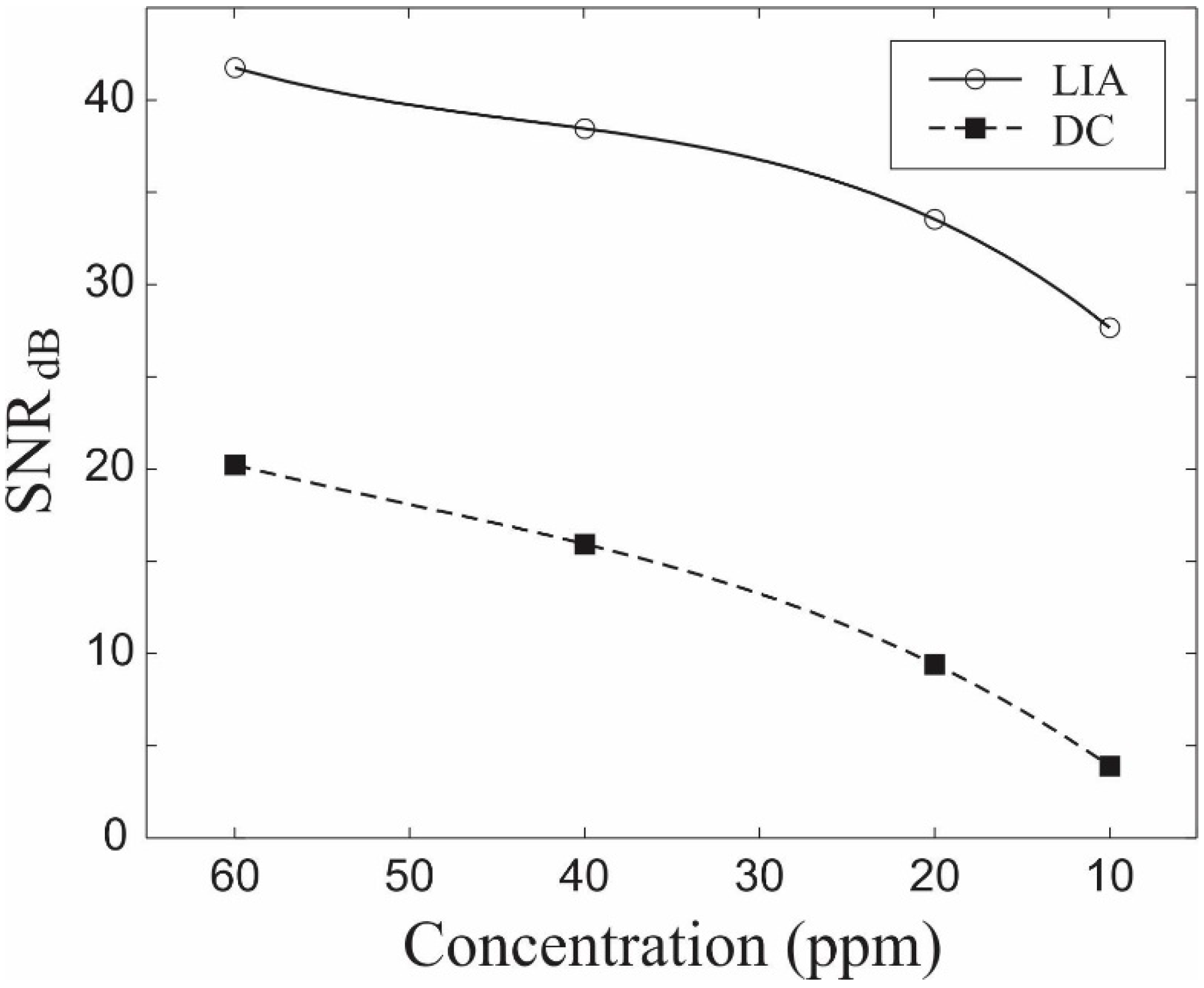
:1. Introduction
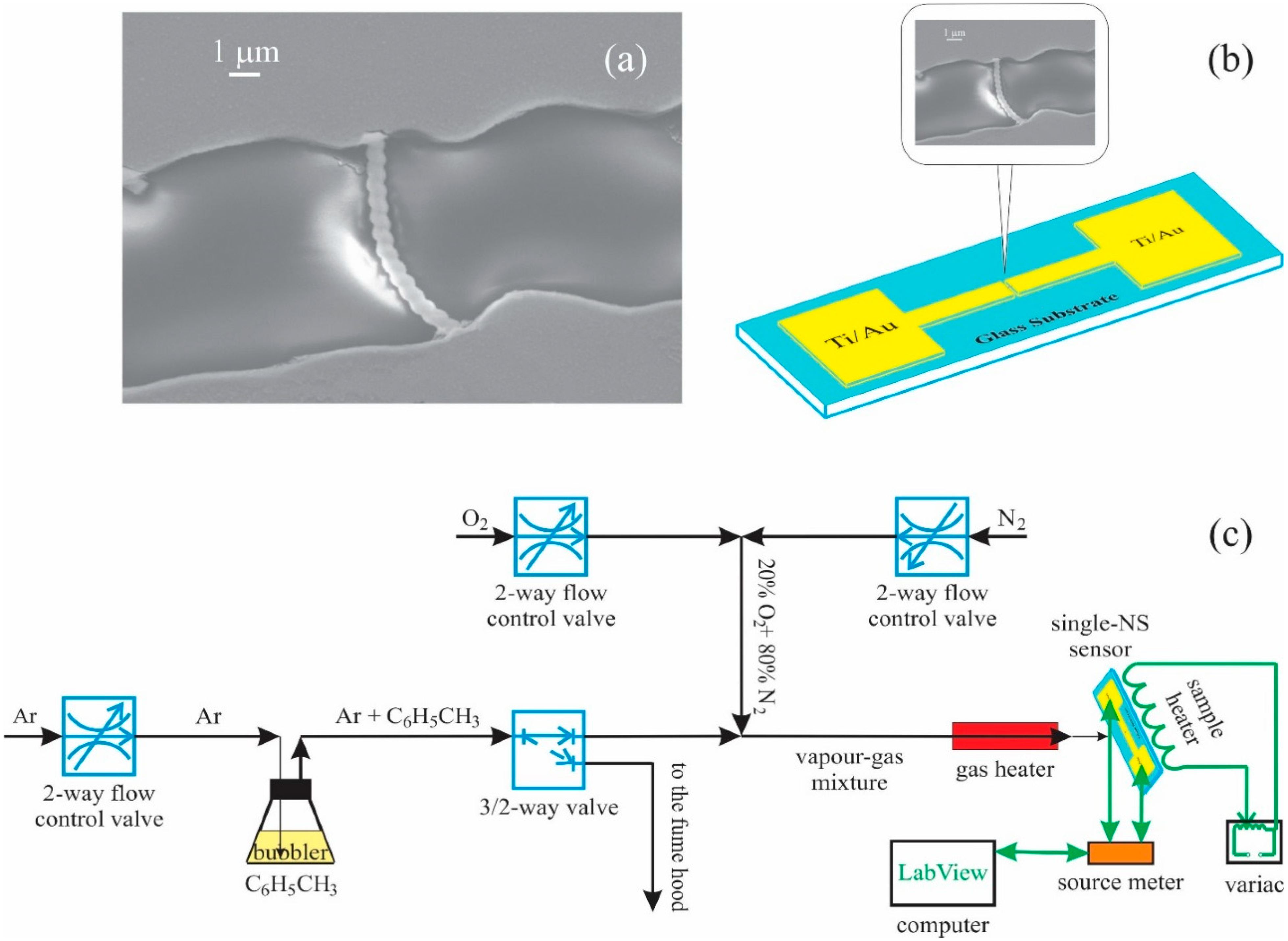
2. Device Fabrication
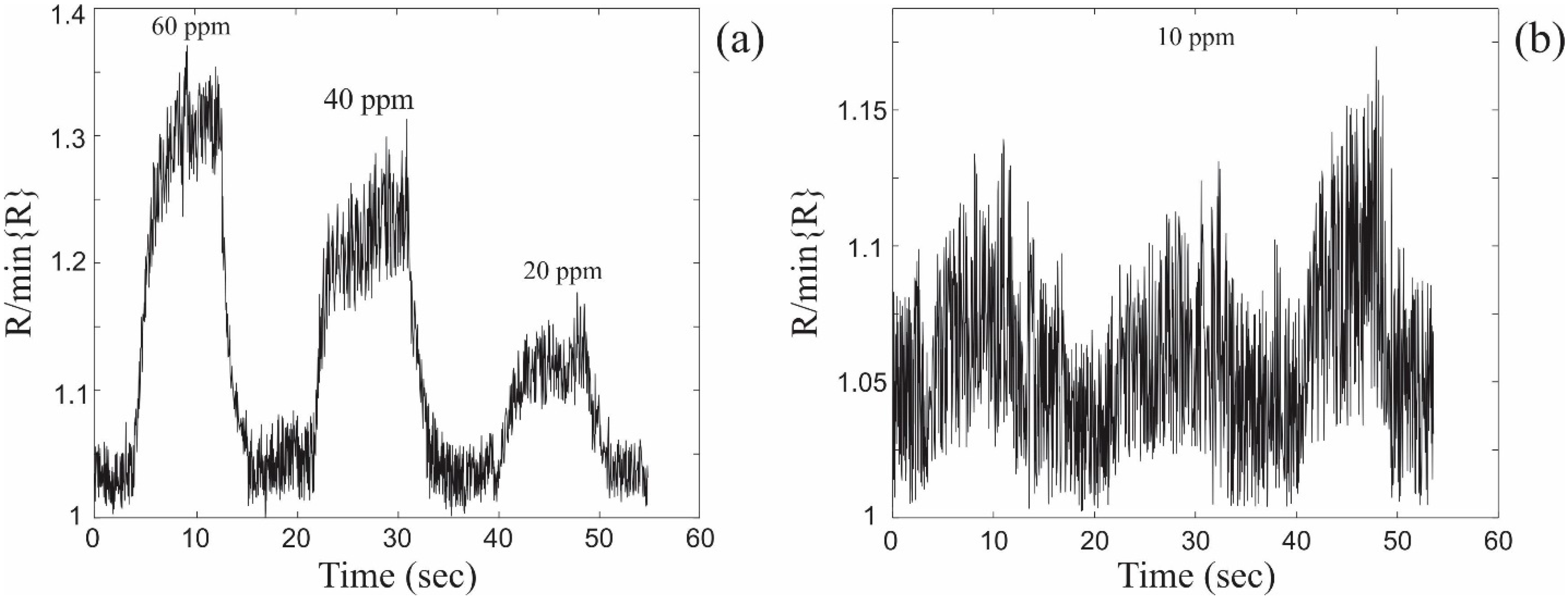
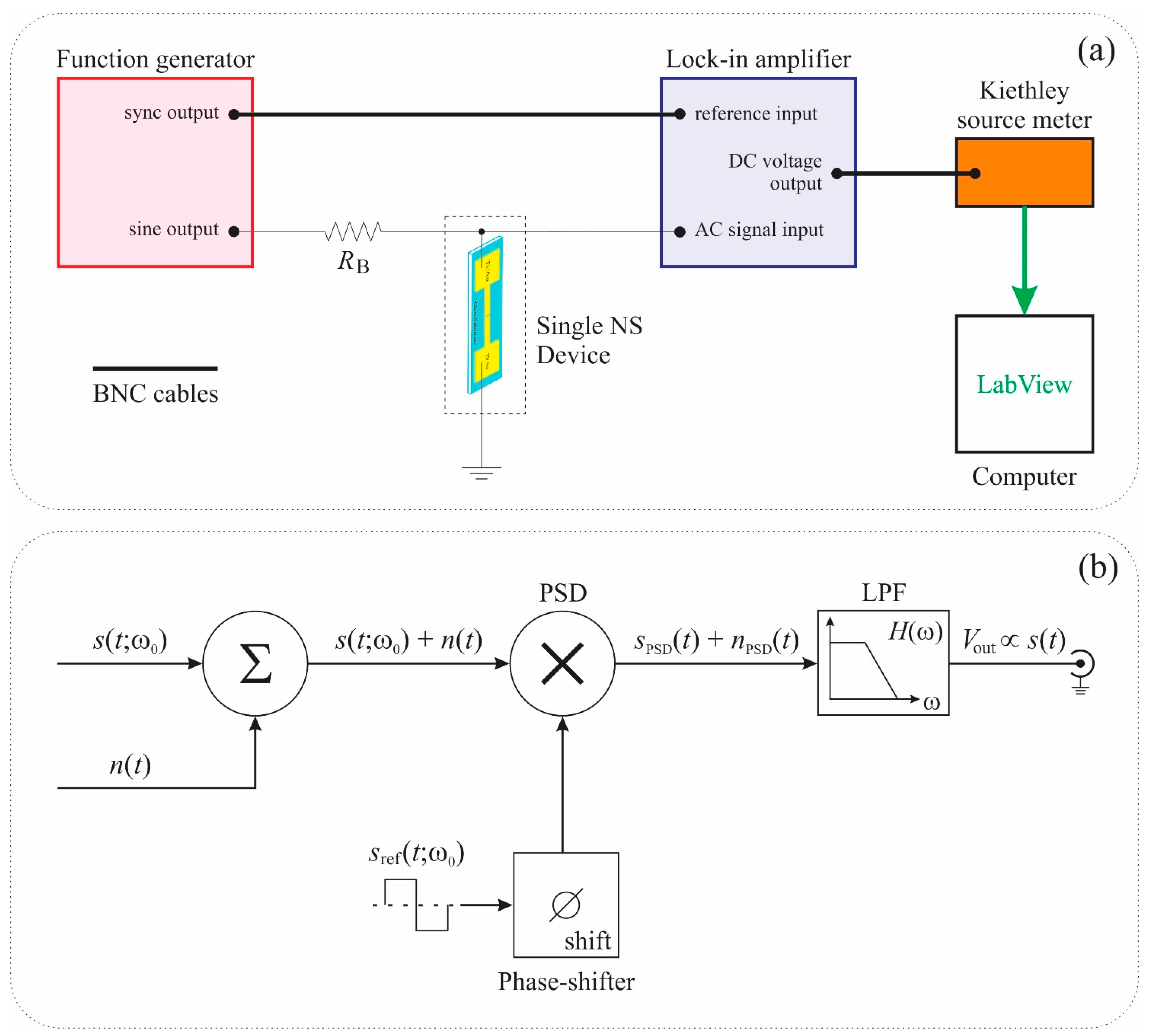
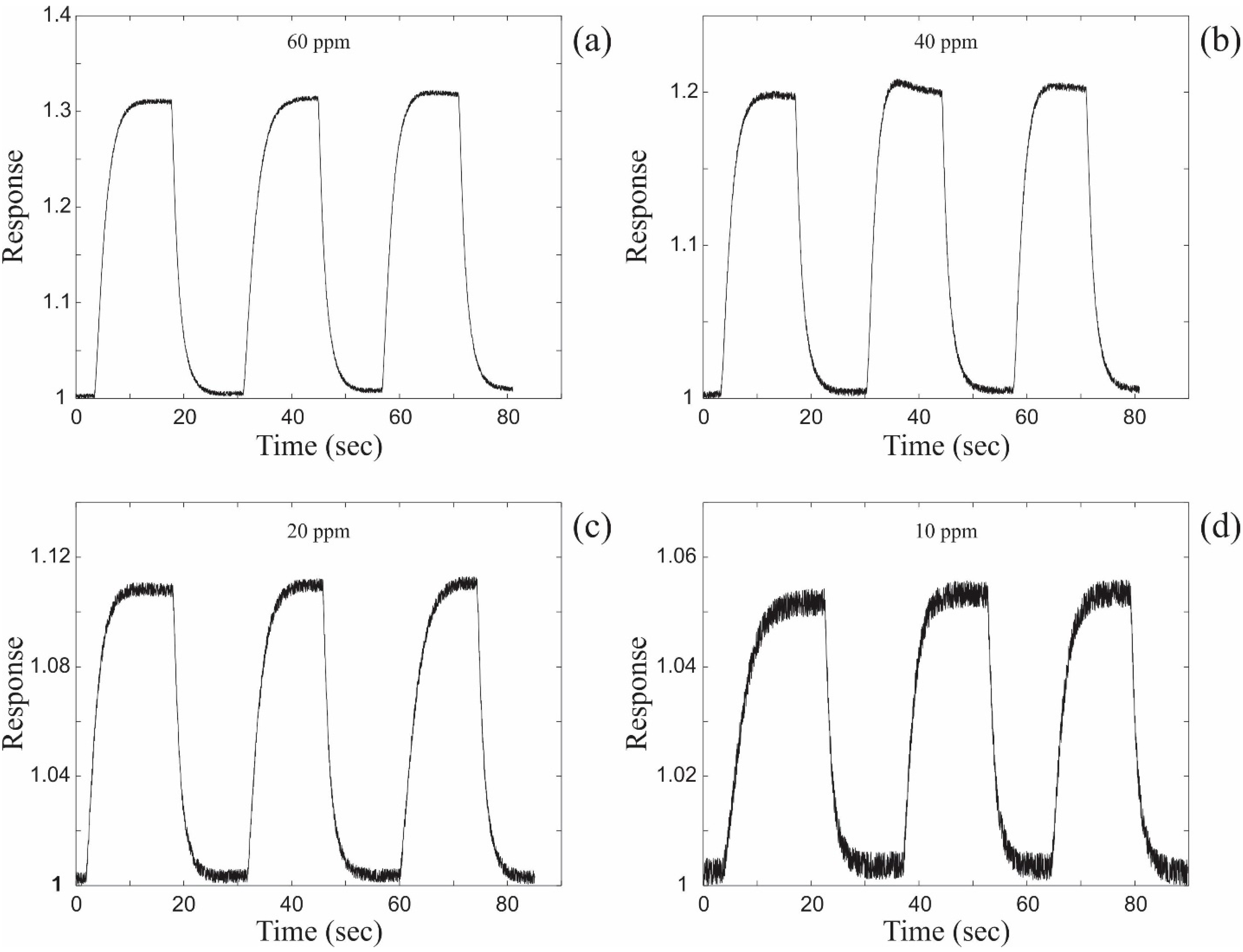
3. Electrical Characterization


4. Conclusions
Acknowledgments
Author Contributions
Conflicts of Interest
References
- Sekhar, P.; Brosha, E.; Mukundan, R.; Garzon, F. Chemical sensors for environmental monitoring and homeland security. ECS 2010, 19, 35–40. [Google Scholar]
- Pejcic, B.; Eadington, P.; Ross, A. Environmental monitoring of hydrocarbons: a chemical sensor perspective. Environ. Sci. Tech. 2007, 41, 6333–6342. [Google Scholar] [CrossRef]
- Bielecki, Z.; Janucki, J.; Kawalec, A.; Mikolajczyk, J.; Palka, N.; Pasternak, M.; Pustelny, T.; Stacewicz, T.; Wojtas, J. Sensors and systems for the detection of explosive devices—An overview. Metrol. Meas. Syst. 2012, 19, 3–28. [Google Scholar] [CrossRef]
- Procek, M.; Stolarczyk, A.; Pustelny, T.; Maciak, E. A Study of a QCM Sensor Based on TiO2 Nanostructures for the Detection of NO2 and Explosives Vapours in Air. Sensors 2015, 15, 9563–9581. [Google Scholar] [CrossRef] [PubMed]
- Bakharev, P.; McIlroy, D. The effect of the periodic boundary conditions of a ZnO-coated nanospring on its surface redox-induced electrical response. Nanotechnology 2014, 25, 475501. [Google Scholar] [CrossRef] [PubMed]
- Bakharev, P.; Dobrokhotov, V.; McIlroy, D. A method for integrating ZnO coated nanosprings into a low cost redox-based chemical sensor and catalytic tool for determining gas phase reaction kinetics. Chemosensors 2014, 2, 56–68. [Google Scholar] [CrossRef]
- Dobrokhotov, V.; Oakes, L.; Sowell, D.; Larin, A.; Hall, J.; Kengne, A.; Bakharev, P.; Corti, G.; Cantrell, T.; Prakash, T.; et al. ZnO coated nanospring-based chemiresistor. J. Appl. Phys. 2012, 111, 044311:1–044311:8. [Google Scholar] [CrossRef]
- Dobrokhotov, V.; Oakes, L.; Sowell, D.; Larin, A.; Hall, J.; Barzilov, A.; Kengne, A.; Bakharev, P.; Corti, G.; Cantrell, T.; et al. Thermal and optical activation mechanisms of nanospring-based chemiresistors. Sensors 2012, 12, 5608–5622. [Google Scholar] [CrossRef] [PubMed]
- Dobrokhotov, V.; Oakes, L.; Sowell, D.; Larin, A.; Hall, J.; Kengne, A.; Bakharev, P.; Corti, G.; Cantrell, T.; Prakash, T.; et al. Toward the nanospring-based artificial olfactory system for trace-detection of flammable and explosive vapors. Sens. Actuators B Chem. 2012, 168, 138–148. [Google Scholar] [CrossRef]
- Sysoev, V.; Goschnick, J.; Schneider, T.; Strelcov, E.; Kolmakov, A. A gradient microarray electronic nose based on percolating SnO2 nanowire sensing elements. Nano Lett. 2007, 7, 3182–3188. [Google Scholar] [CrossRef] [PubMed]
- Bochenkov, V.; Sergeev, G.; Bochenkov, V.; Sergeev, G. Metal Oxide Nanostructures and Their Applications, 2nd ed.; Umar, H., Ed.; American Scientific Publishers: Valencia, CA, USA, 2010; Volume 3, pp. 31–52. [Google Scholar]
- Liu, X.; Cheng, S.; Liu, H.; Hu, S.; Zhang, D.; Ning, H. A survey on gas sensing technology. Sensors 2012, 12, 9635–9665. [Google Scholar] [CrossRef] [PubMed]
- Barsan, N.; Weimar, U. Conduction model of metal oxide gas sensors. J. Electroceram. 2001, 7, 143–167. [Google Scholar] [CrossRef]
- Barsan, N.; Weimar, U. Understanding the fundamental principles of metal oxide based gas sensors; the example of CO sensing with SnO2 sensors in the presence of humidity. J. Phys. Condens. Matter 2003, 15, R813–R839. [Google Scholar] [CrossRef]
- Gurlo, A.; Bârsan, N.; Oprea, A.; Sahm, M.; Sahm, T.; Weimar, U. An n- to p-type conductivity transition induced by oxygen adsorption on a-Fe2O3. Appl. Phys. Lett. 2004, 85. [Google Scholar] [CrossRef]
- Ra, H.; Khan, R.; Kim, J.; Kang, B.; Im, Y. The effect of grain boundaries inside the individual ZnO nanowires in gas sensing. Nanotechnology 2010, 21. [Google Scholar] [CrossRef] [PubMed]
- Li, Q.; Gao, T.; Wang, Y.; Wang, T. Adsorption and desorption of oxygen probed from ZnO nanowire films by photocurrent measurements. Appl. Phys. Lett. 2005, 86, 123117:1–123117:3. [Google Scholar] [CrossRef]
- Gas’kov, A.; Rumyantseva, M. Nature of gas sensitivity in nanocrystalline metal oxides. J. Appl. Chem. 2001, 74, 440–444. [Google Scholar]
- McIlroy, D.; Alkhateeb, A.; Zhang, D.; Aston, D.; Marcy, A.; Norton, M. Nanospring formation—Unexpected catalyst mediated growth. J. Phys. Condens. Matter 2004, 16, R415–R440. [Google Scholar] [CrossRef]
- Wang, L.; Major, D.; Paga, P.; Zhang, D.; Norton, M.; McIlroy, D. High yield synthesis and lithography of silica-based nanospring mats. Nanotechnology 2006, 17, S298–S303. [Google Scholar] [CrossRef]
- George, S.; Ott, A.; Klaus, J. Surface chemistry for atomic layer growth. J. Phys. Chem. 1996, 100, 13121–13131. [Google Scholar] [CrossRef]
- Guziewicz, E. ZnO by ALD-advantages of the material grown at low temperature. Acta Phys. Pol. A 2009, 116, 814–817. [Google Scholar]
- Seguin, J.-L.; Gomri, S.; Guerin, J.; Aguir, K. Bases of noise spectroscopy for enhancing metallic oxide gas sensors selectivity. In Science and Technology of Chemiresistor Gas Sensors; Aswal, K.D., Gupta, S.K., Eds.; Nova Science Publishers Inc.: New York, NY, USA, 2007; pp. 351–371. [Google Scholar]
- Konczakowska, A.; Wilamowski, B. Noise in semiconductor devices. In Fundamentals of Industrial Electronics, 2nd ed.; CRC Press: Boca Raton, FL, USA, 2011. [Google Scholar]
- Christensson, S.; Lundstrom, I.; Svensson, C. Low frequency noise in MOS transistors-I theory. Solid-State Electron. 1968, 11, 797–812. [Google Scholar] [CrossRef]
- Bertz, F. Theory of low frequency noise in Si MOST’s. Solid-State Electron. 1970, 3, 631–647. [Google Scholar] [CrossRef]
- Hsu, S. Surface state related 1/f noise in MOS transistors. Solid-State Electron. 1970, 13, 1451–1459. [Google Scholar] [CrossRef]
- McWhorter A 1/f noise and germanium surface properties. In Semiconductor Surface Physics; University of Philadelphia Press: Philadelphia, PA, USA, 1957; p. 207.
- Hooge, F. 1/f noise. Physica 1976, 83B, 14. [Google Scholar] [CrossRef]
- Fan, Z.; Lu, J.G. Zinc oxide nanostructures: synthesis and properties. J. Nanosci. Nanotechnol. 2005, 10, 1561–1573. [Google Scholar] [CrossRef]
- Kanno, I.; Kotera, H.; Wasa, K. Measurement of transverse piezoelectric properties of PZT thin films. Sens.Actuators A Phys. 2003, 107, 68–74. [Google Scholar] [CrossRef]
- Sysoev, V.; Strelcov, E.; Kolmakov, A. Multidimensional micro-arrays based on metal oxide nanowires for electronic nose application. In Integrated Analytical Systems; Springer: New York, NY, USA, 2013; pp. 465–502. [Google Scholar]
- Tripathy, A.; Mohanty, A.; Mohanty, M. Electronic nose for black tea quality evaluation using kernel based clustering approach. Int. J. Image Process. 2012, 6, 86–93. [Google Scholar]
- Brudzewski, K.; Osowski, S.; Dwulit, A. Recognition of coffee using differential electronic nose. IEEE Trans. Instrum. Meas. 2012, 61, 1803–1810. [Google Scholar] [CrossRef]
© 2015 by the authors; licensee MDPI, Basel, Switzerland. This article is an open access article distributed under the terms and conditions of the Creative Commons Attribution license (http://creativecommons.org/licenses/by/4.0/).
Share and Cite
Bakharev, P.V.; McIlroy, D.N. Signal-to-Noise Enhancement of a Nanospring Redox-Based Sensor by Lock-in Amplification. Sensors 2015, 15, 13110-13120. https://0-doi-org.brum.beds.ac.uk/10.3390/s150613110
Bakharev PV, McIlroy DN. Signal-to-Noise Enhancement of a Nanospring Redox-Based Sensor by Lock-in Amplification. Sensors. 2015; 15(6):13110-13120. https://0-doi-org.brum.beds.ac.uk/10.3390/s150613110
Chicago/Turabian StyleBakharev, Pavel V., and David N. McIlroy. 2015. "Signal-to-Noise Enhancement of a Nanospring Redox-Based Sensor by Lock-in Amplification" Sensors 15, no. 6: 13110-13120. https://0-doi-org.brum.beds.ac.uk/10.3390/s150613110