1. Introduction
Delay-Locked Loops (DLLs) with high-resolution delay steps are extensively used for time management of large systems [
1]. For example, they are used in Fluorescence Lifetime Imaging Microscopy (FLIM) sensors where a light pulse is modulated with the capture window that is shifted in picosecond-order delay steps for a total range of tens of picoseconds [
2]. Furthermore, high-resolution DLLs are used in the compensation for PVT variations and any delay mismatch that may be caused to signals during the operation of many high-frequency VLSI circuits [
3]. For all of these applications, DLLs should generate an adequate amount of lock/delay range while maintaining the output jitter as low as possible. This is because there is a trade-off relation between delay range and the jitter performance [
4]. In addition, the total delay fluctuations including jitter should be less than the delay resolution for optimum operation [
5].
Since DLLs only adjust the phase (delay) of an input signal and not its frequency, DLLs suffer from limited delay range. Therefore, a considerable amount of new techniques has been developed to address this issue. For example, a technique employing a Digital-to-Analog Converter (DAC) with Parallel Variable Resistor (PVR) is used to realize high-resolution delay steps with a wide delay range by accurately controlling the Current-Controlled Delay Element (CCDE) of the DLL [
1]. Another technique developed is the use of a dual-loop architecture which utilizes multiple delay lines [
6]. The first “reference” loop generates a clock with quadrature phases. In the second “main” loop, these phases are delayed by four Voltage-Controlled Delay Lines (VCDLs) and then multiplexed to generate the output clock. A new technique based on cycle-controlled delay unit was proposed by [
7] to enlarge the delay range by reusing the delay units in a cycle-like process without the need for cascading a large number of delay units. A DLL with a new voltage-controlled delay element based on body-controlled current source and body-feed technique was also developed to widen the delay range [
8]. In this method, the Phase Detector (PD) is replaced by a Phase/Frequency Detector (PFD) with a start controller to achieve a sufficient locking range. Another new architecture was proposed by [
9] which employs a mixed-mode Time-to-Digital Converter (TDC) for enabling a frequency-range selector. The frequency-range selector can generate digital control signals to switch the delay range of the multi-controlled delay cell in the VCDL and the current of the digitally-controlled charge pump.
However, the majority of the techniques mentioned above result in complex circuit architectures that lead to degraded jitter performance as well as increased area overhead, cost, and power consumption. Motivated by this research gap, this work proposes a new and simple technique using a Capacitor-Reset Circuit (CRC) to reset the loop filter capacitor for delay range extension and at the same time reducing the jitter performance into the sub-picosecond range. The capacitor-reset technique is widely used to reinitialize a control voltage to a fixed initial value and has been applied in many circuits such as pixels of image sensors and PLL circuits [
10,
11]. At this point, mathematical analysis confirmed by circuit simulation, our proposed technique is capable of generating a comparably wide delay range and picosecond-resolution delay steps with a sub-picosecond jitter performance. In addition, this architecture consumes a relatively small area and power compared with the available techniques reported in literature.
Table 1 below shows performance specifications of the most recent and relevant high-resolution DLL designs reported in the literature.
Table 1 summarizes the DLL’s parameters that have a direct impact on the performance in terms of speed and power consumption. For example, information about achievable delay range, delay resolution, number of delay steps, operating frequency range, RMS jitter, and power consumption is provided in
Table 1. It is worth noting that the finest delay step is 4 ps achieved by [
12]. It also generates a comparably long delay range of approximately 345 ps.
The proposed design is explained in the subsequent section. The results and discussion are presented in
Section 3. Finally,
Section 4 summarizes and concludes this paper.
2. Materials and Methods
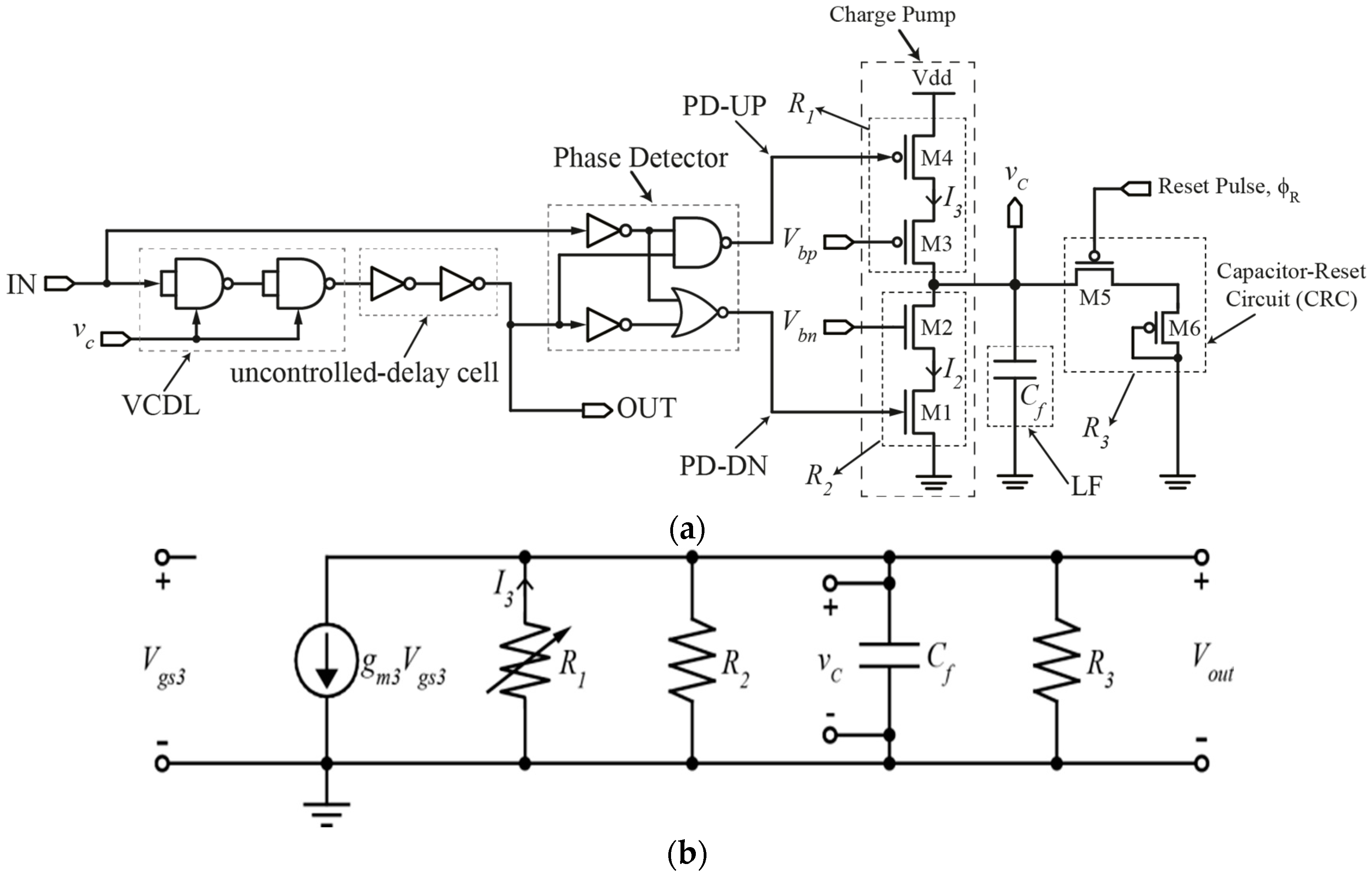
Our proposed circuit is shown in
Figure 1a. It consists of a conventional VCDL, an Exclusive-OR (XOR) gate-based Phase Detector (PD), a Charge Pump (CP), and a modified Loop Filter (LF) with the addition of the CRC. It works by resetting the loop filter’s capacitor by a pre-determined time constant before lock is achieved. The reset operation is performed by a reset signal, ϕ
R. By varying the pulse width of ϕ
R using a simple Pulse-Width Generator (PWG) circuit that will be illustrated at the end of this section, a change in the time constant
τR of the modified loop filter is achieved. This results in a change in delay range of the DLL.
Figure 1a shows the modification made to the loop filter of a DLL where M5 and M6 are used to create the CRC. M5 acts as a switch that resets the loop filter’s capacitor,
Cf. On the other hand, M6 is connected as a diode whose resistance together with the capacitance
Cf of the loop filter’s capacitor creates a time constant
τR that controls the magnitude of
vc which is fed to the VCDL current to control bias current and propagation delay. This ultimately controls the delay step and lock/delay range. The aspect ratio of both pMOS transistors, M5 and M6, is 0.35 μm/0.13 μm.
The capacitor-reset operation at a pre-determined reset signal duration results in a varying charge/discharge rate of
Cf when
Vbp is changed as opposed to a DLL without the CRC. This results in changes in
vc settling time that controls the delay of the VCDL. To illustrate this operation, the charge pump’s small-signal model shown in
Figure 1b is used.
vc is expressed in Equations (1) and (2) during charging and discharging operations, respectively.
where
vch0,
vdis0, and
τR are the initial voltage across
Cf during charging (which is equal to −
VTp), initial voltage across
Cf during discharging (which is equal to maximum
vc), and the time constant of the loop filter, respectively. This time constant,
τR, is written as:
where
R3 is the equivalent resistance of the diode-connected transistor’s (M6) output resistance in series with transistor M5’s output resistance.
From Equations (1) and (2), it is obvious that the capacitor’s voltage
vc is directly dependent on charging/discharging time,
t. Equations (1) and (2) also implies that the charging/discharging time of
Cf can be changed by changing the time constant
τR of the CRC, which will in turn change
vc. This is achieved through changing the reset duration of the reset signal ϕ
R that is applied to the gate of M5 (see
Figure 1a).
The small-signal model of the charge pump connected to the CRC shown in
Figure 1b is also used to analyze how the DLL generates fine-linear delay steps within a selectable delay range.
Vbp is varied in order to vary the delay steps. The series output resistance of transistors M4 and M3 is modeled as
R1 in
Figure 1b. Likewise,
R2 in
Figure 1b models the series output resistance of transistors M2 and M1 and
R3 models the output resistance of the diode-connected transistor M6 in series with transistor M5’s output resistance when M5 is turned on. It should be mentioned that the aspect ratio of the nMOS transistors M1 and M2 is 0.6 μm/0.13 μm, and that of the pMOS transistors M3 and M4 is 1.2 μm/0.13 μm. The value of the capacitance
Cf in
Figure 1a,b is 0.63 fF.
R1,
R2 and
R3 are given by Equations (4)–(6), respectively [
16]:
When
Vbp is varied, it is obvious that
rds3 and
gm3 change accordingly, resulting in a change in
R1. Due to this,
R1 is written as:
where
∆rds3 and
∆gm3 are the changes in
rds3 and
gm3, respectively. Equation (7) represents the change in
R1 when
Vbp ≠ 0 and can also be written in the following form:
where
RC0 is a constant corresponding to the term (
gm3rds3rds4) and
RP is a variable corresponding to the term (
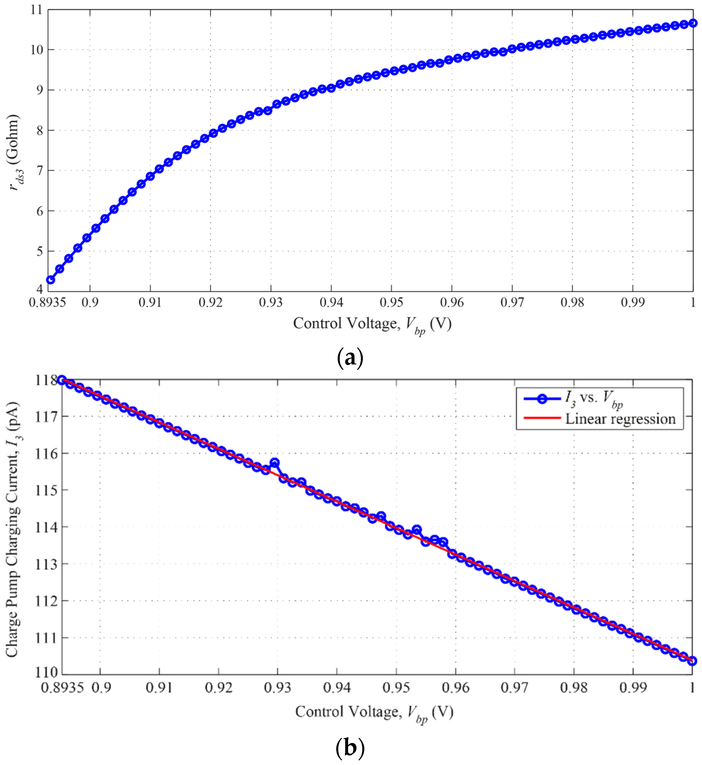
rds4(gm3∆rds3 + rds3∆gm3 + ∆rds3 ∆gm3)) in Equation (7). According to simulation results shown in
Figure 2, when
Vbp is varied from 1 V to 0.8935 V,
Δrds3 changes from 10.66 GΩ to 4.29 GΩ. Likewise, for the same
Vbp range, the charge pump’s charging current
I3 changes from 110.37 pA to 117.99 pA. However, when
Vbp = 0,
rds3 and
gm3 are at their minimum values. This implies that
∆rds3 and
∆gm3 will have very small values which can be neglected compared with other
R1 cases in which
Vbp ≠ 0. Hence, Equation (8) can be rewritten as:
where
R1,0 represents the case when
Vbp = 0. Thus, Equation (8) can be rewritten as follows:
It should be mentioned that the non-monotonicity points in
Figure 2b can be a consequence of the non-convergence problems. These problems can be caused during the simulation if the resistance of the transistor is very high or very low. This can be solved by adjusting either the simulator options or the transistor model parameters (Ron and/or transconductance
gm) [
17]. However, no significant impact can be observed in the overall behavior and performance of the DLL circuit, as will be demonstrated in the delay steps linearity results explained in the next section. In addition, a linear regression has been employed and superimposed on the plot in
Figure 2b regarding the charge pump charging current
I3 versus the control voltage
Vbp. It can be seen from
Figure 2b that the Root-Mean Square Error (RMSE) of the linear regression plot is only 0.06, which indicates that the original plot of
I3 versus
Vbp is almost linear.
According to [
1], the relationship between the change in resistance and the change in current is expressed as:
The time delay,
td, of the VCDL is given as [
18]:
where
Tref,
KVCDL, and
∆d are the period time of the input clock signal, the gain of the VCDL, and the jitter caused by the VCDL, respectively. Equation (12) indicates that the voltage,
vc, across the capacitor determines the time delay,
td. The voltage
vc can be written as [
18]:
Substituting Equation (13) into Equation (12),
td is written as:
Substituting Equation (11) for
I3 into Equation (14) yields
td in terms of the change in
R1 and
I3 and is written as:
td in Equation (15) represents the delay step. On the other hand, the delay range,
tdr, is defined as the difference between maximum and minimum delays and can be written as:
where
td(max) and
td(min) are the maximum and the minimum delays. On the other hand, the maximum and minimum delays are expressed by Equations (17) and (18), respectively:
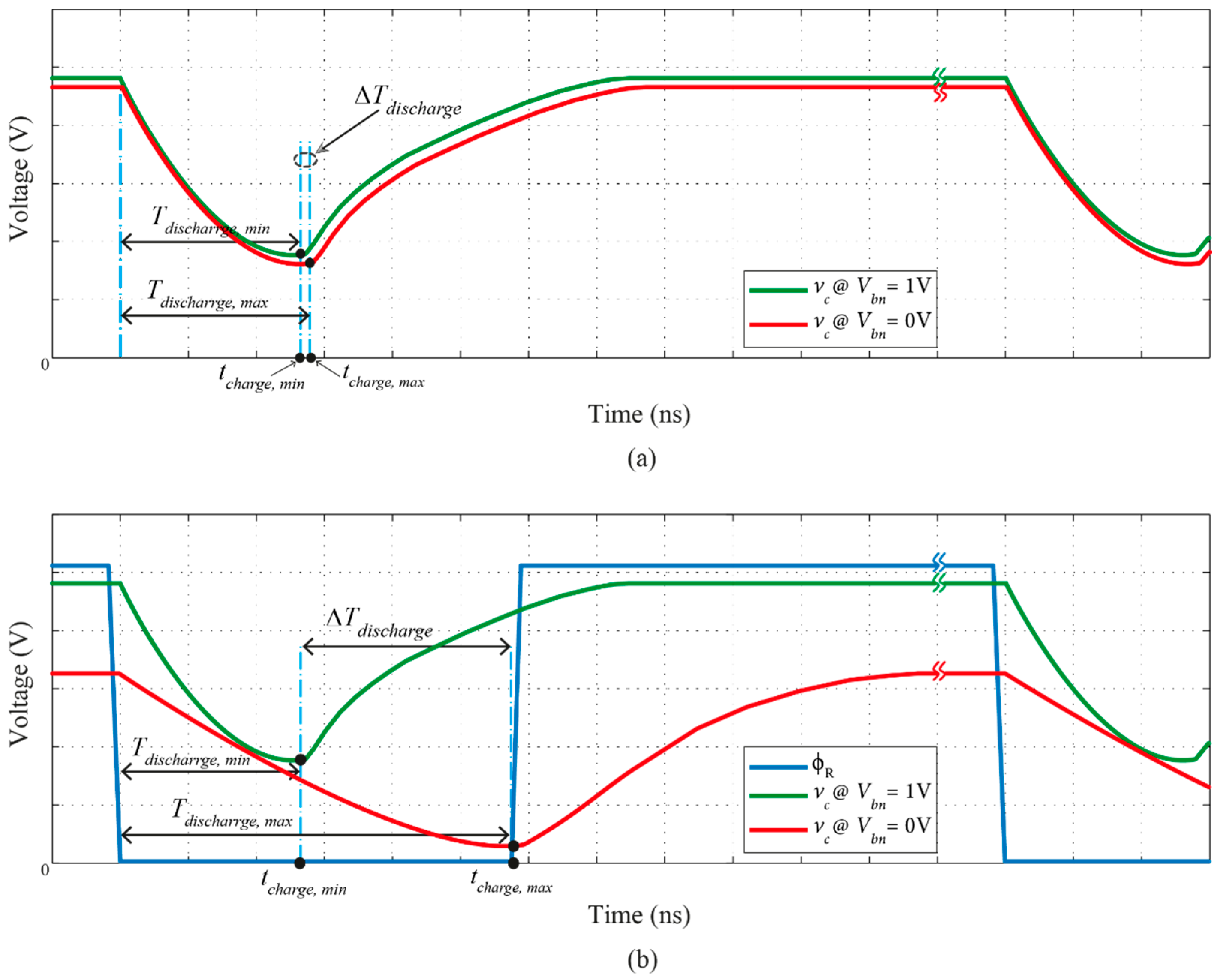
In order to demonstrate the operation of the charge pump circuit without and with the proposed CRC technique,
Figure 3 is considered. This figure is an illustration figure that illustrates the differences in the discharge rates for two extreme values of
Vbn (1 V and 0 V).
Figure 3a highlights the discharge rates for a charge pump without the proposed CRC and
Figure 3b with the CRC. It is obvious from
Figure 3b that the difference in discharge rates is significantly higher than that of the case in
Figure 3a. To clarify this, according to the simulations, the discharge rates’ difference for the case with the CRC technique is 2.49 mV/ps, while that for the case without CRC is only 0.2 mV/ps. The higher is the difference in the discharge rate, the bigger is the difference in
vc settling values according to Equations (1), (2), (15), (17) and (18). In relation to the simulation results, the discharge rate of
vc is faster when
Vbn value is 1 V, causing the capacitance
Cf to fully discharge faster and the discharging time to have a lower value compared to the case when
Vbn is 0 V. The discharge rate is directly proportional to the discharge current
I2. Since the discharge rate is different, the settling voltage for
vc is also different, causing a change in the control voltage of the VCDL and resulting in a change in time delay of the DLL.
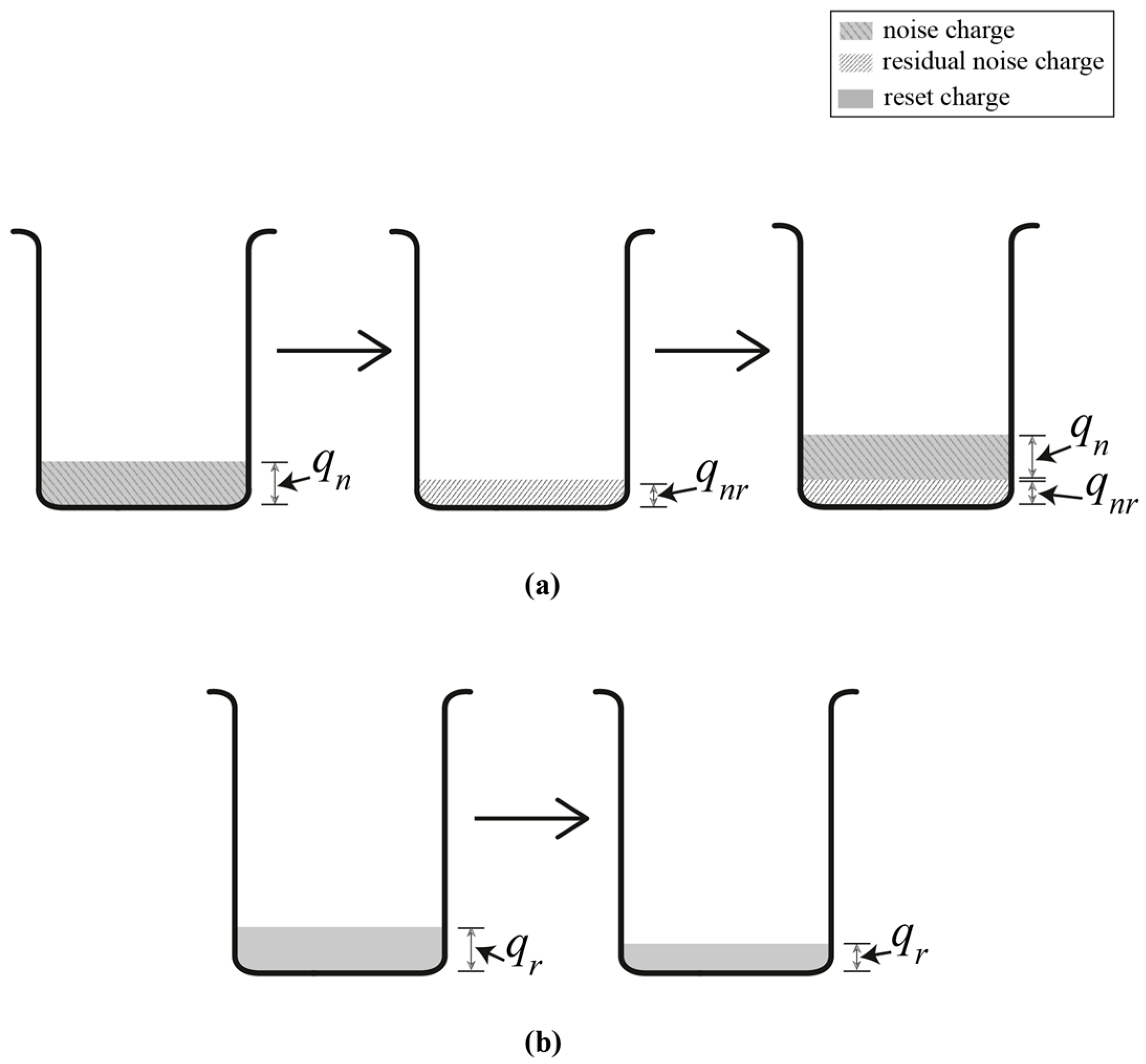
The charge pump circuit of a DLL suffers from amplifier noise charge injected from its amplifier into the loop filter capacitor, thus reducing this noise will result in better time jitter performance [
19].
Figure 4 is used to illustrate error charge accumulation in charge pump’s loop filter capacitor.
Figure 4a shows a conventional charge pump where initially amplifier noise charge
qn is injected into
Cf from the amplifier at the ON phase of the input signal. When the input signal goes low,
Cf discharges but a small amount of residual noise charge
qnr is left in C
f. The next ON phase of the input signal injects new amplifier noise charge and it is added with the residual noise charge left from the previous discharge cycle. Therefore, for simplicity, the output voltage
vc of the charge pump, is given by:
The numerator of Equation (19) gives the total noise charge of a conventional charge pump. On the other hand,
Figure 4b shows that noise charge is also transferred into the loop filter's capacitor. However, when the signal goes high, the CRC is activated and causes
Cf to fully discharge. Only a small amount of reset charge
qr is injected into
Cf from transistors M5 and M6 that make up the CRC (see
Figure 1a). Thus, the output voltage
vc of the charge pump is given by:
We can also view qr as noise charge since it is random in nature. However, qr is much less than qn + qnr, thus the jitter of vc is significantly reduced for a charge pump with the CRC. Moreover, this technique also produces a wider delay range since a larger and accurate level of vc can be achieved when the ON phase period of the reset signal ϕR is made longer through the PWG circuit.
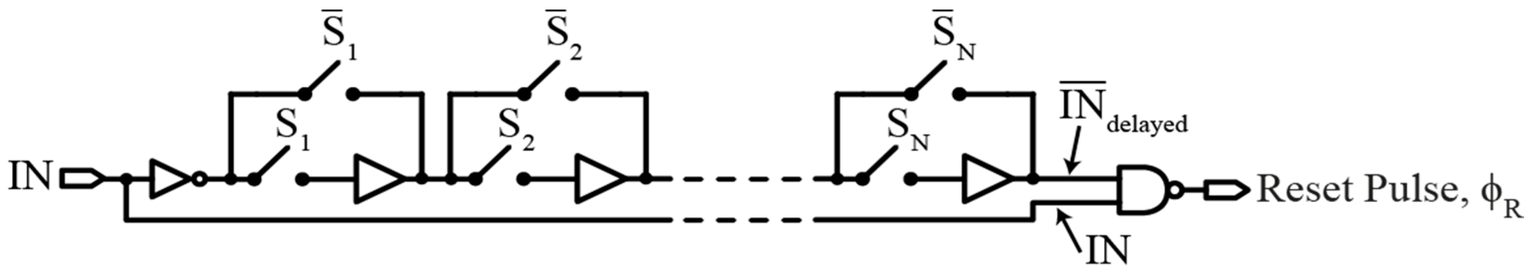
The PWG circuit, used to control the pulse width of the reset signal ϕ
R, is shown in
Figure 5. This circuit is used to set the time constant of the loop filter in order to set the desired discharge rate of
Cf (see Equations (1) and (2)). Once a desired delay range is acquired, the charge pump’s charging current
I3 can be varied through the charge pump amplifier’s bias voltage,
Vbp (see
Figure 1a), to allow small-linear changes in the DLL’s output signal time delay.
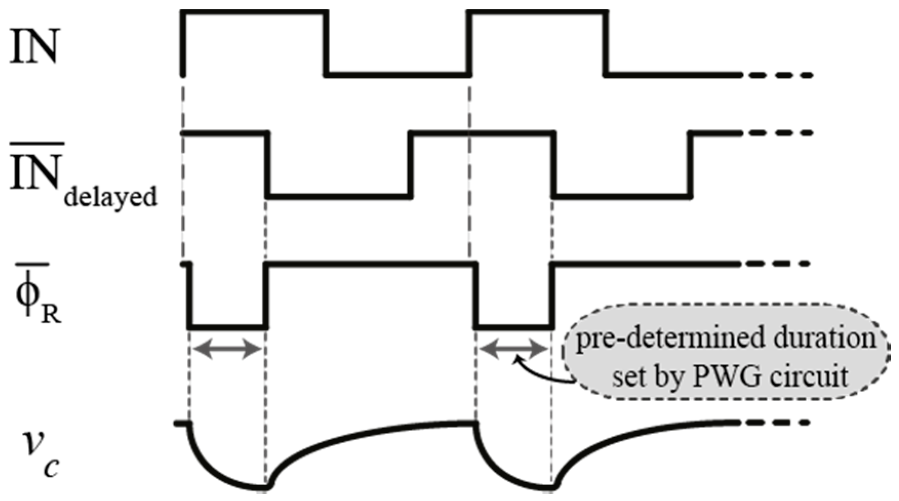
It is also noted that the input of the PWG circuit shown in
Figure 5 is fed from the input signal of the DLL itself in order to synchronize the discharge time of node
vc with the input pulse, as illustrated in the timing diagram shown in
Figure 6.
3. Results and Discussion
The proposed DLL is simulated using a 0.13 µm CMOS process. The power supply voltage is 1.2 V. From post-layout simulations, the delay is controlled from zero to 69 ps by varying Vbp from 0.8935 V to 1 V in steps of 1.5 mV. In this simulation, parametric analysis was used to change Vbp; however, the value of Vbp can be controlled by a 10-bit Digital-to-Analog Converter (DAC). Vbn is fixed at 0.2 V.
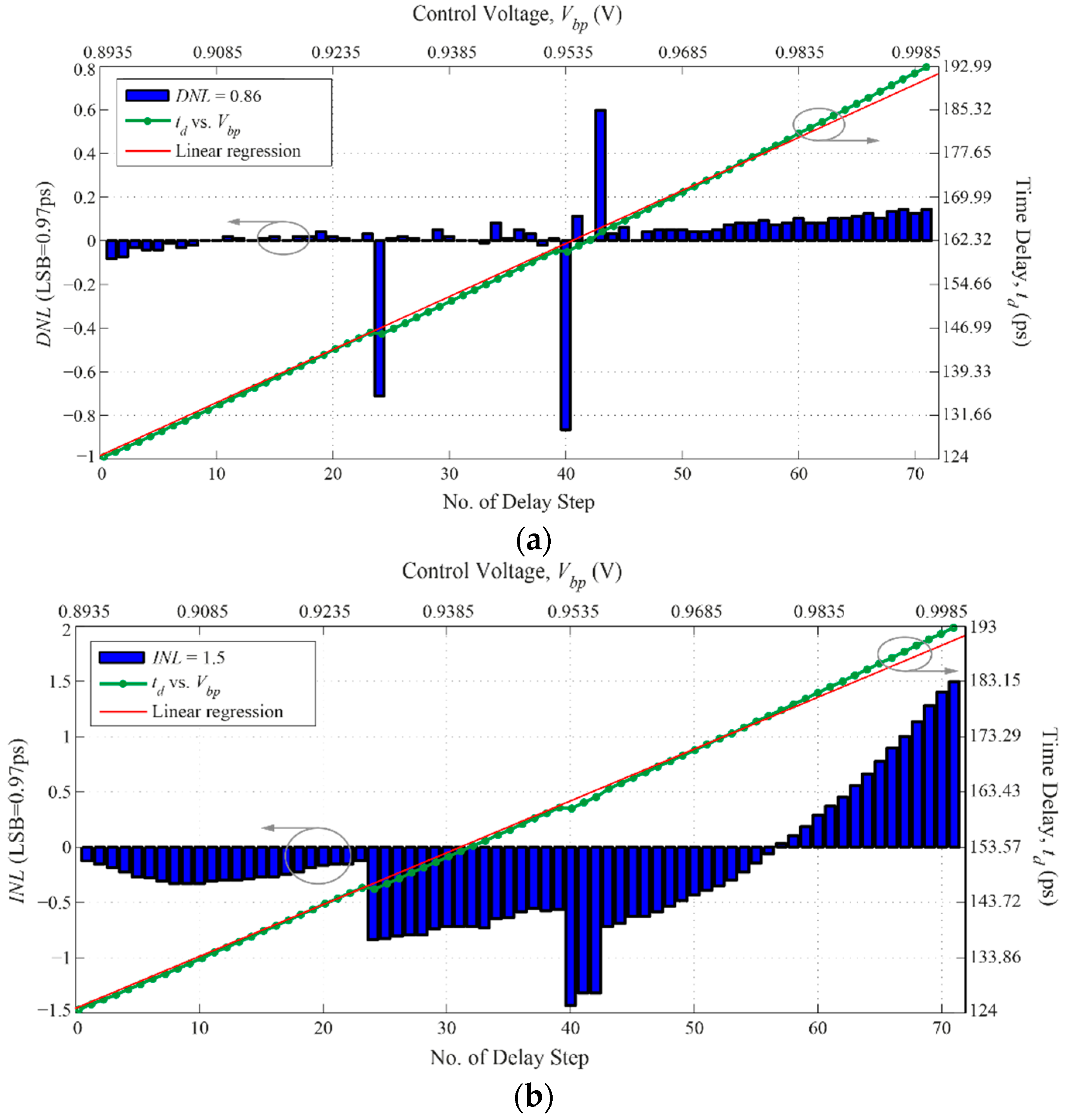
Figure 7 shows the generated output time delay
td as a function of the control voltage
Vbp with respect to the delay steps linearity. It is clear from
Figure 7 that the time delay increases linearly with the increase in
Vbp. The sensitivity of the linear regression plot is approximately 644 (ps/V) with Root-Mean Square Error (RMSE) equals to 0.64. For an LSB of 0.97 ps, it can be seen in
Figure 7a that the delay steps’
Differential Non-Linearity (DNL) does not exceed 0.86. Moreover, the
DNL values of the delay steps located between the 41st and 70th delay steps are all concentrated in the positive region. This has mainly caused the slight deviation observed between the linear regression and the simulated output delay steps shown in
Figure 7a,b, and it has also resulted in the maximum 1.5
Integral Non-Linearity (
INL) value at the end of the
INL plot in
Figure 7b. On the other hand, the
INL values across the generated delay steps in
Figure 7b are somewhat concentrated in the negative region. This indicates that the resolution of most of the delay steps is very close to one LSB of the output delay.
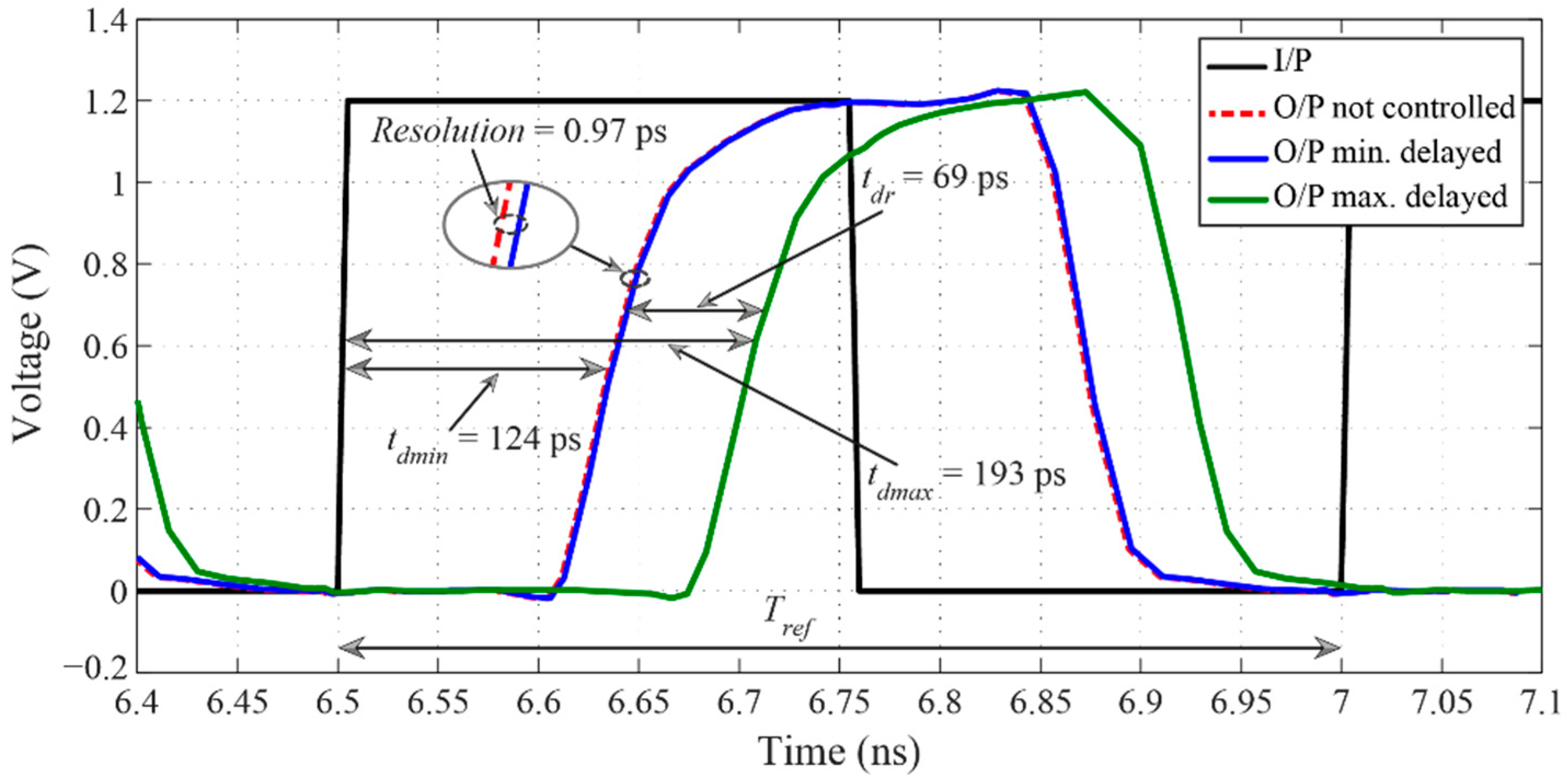
Figure 8 shows the simulated DLL’s output signal, which is delayed by 0.97 ps as the minimum delay step and total of 69 ps as the maximum delay range, when operated at 2 GHz of the input reference signal. The lock-in time of the DLL is only 14 cycles.
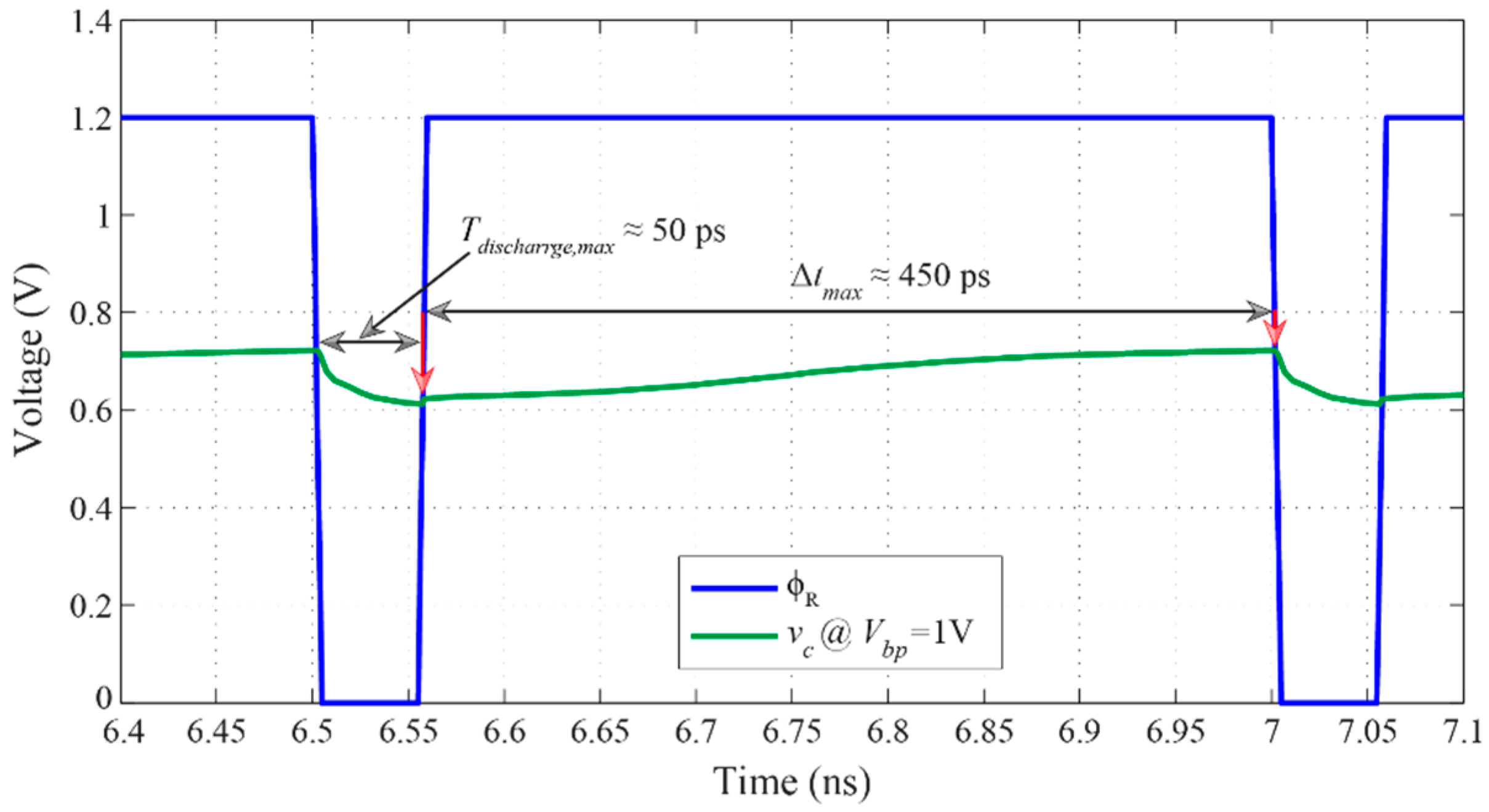
Figure 9 shows the simulated voltage
vc across the loop filter’s capacitor with the reset signal ϕ
R.
It can be seen in
Figure 9 that the duration of the reset signal ϕ
R is almost identical to the maximum discharge time,
Tdischarge,max, obtained when
Vbp equals to 1 V. The waveforms plotted in
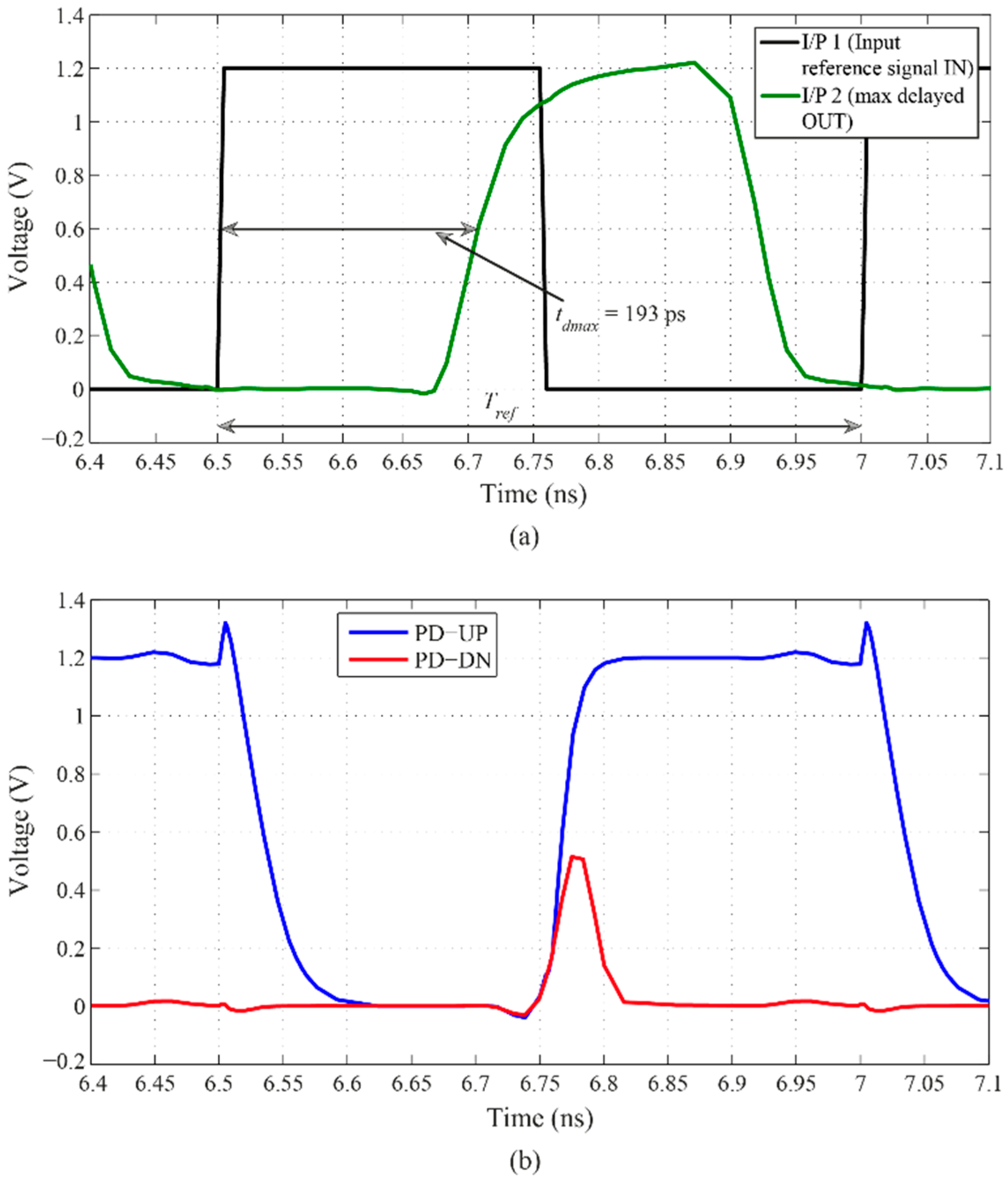
Figure 9 have been obtained after the locked state has been achieved, i.e., after 14 cycles. Likewise, at locked state and when
Vbp equals to 1 V, the input and output signals of the phase detector are presented in
Figure 10.
Figure 10a shows the input reference and output delayed signals which are fed to the two inputs of the phase detector. According to the phase difference between these two inputs, the phase detector generates phase difference information, signal “PD-UP” and signal “PD-DN” in
Figure 10b, which is fed to the charge pump to keep the operation of the DLL in the locked state.
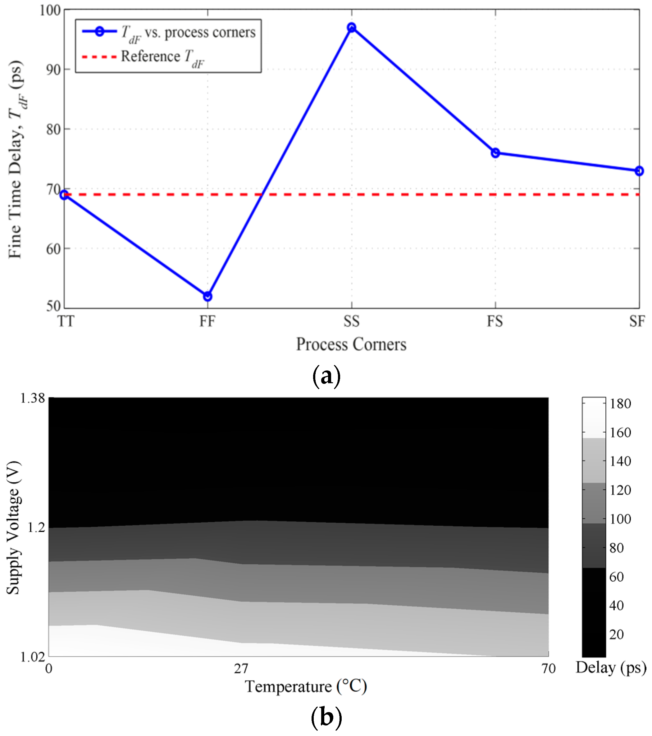
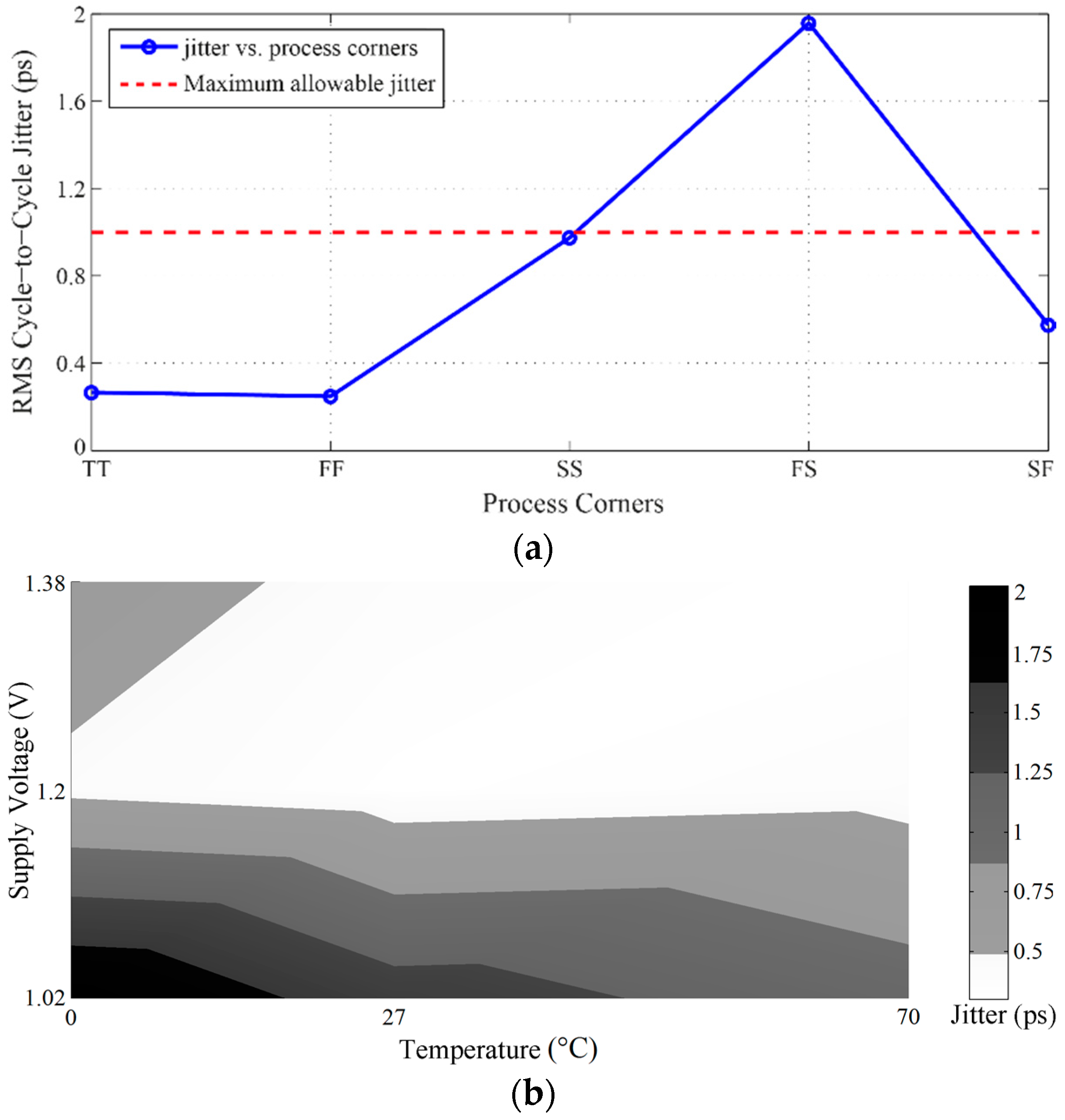
For completeness, the PVT variations effects on the DLL’s delay range have been simulated and analyzed, as shown in
Figure 11. Since the maximum achievable delay range is 69 ps, it can be noted in
Figure 11a that the process corner FF can degrade the delay range and the corner SS can mostly degrade the jitter through the extremely extended range. Nonetheless, extending or narrowing the pulse width of the reset pulse, ϕ
R, can solve these shortcomings. In
Figure 11b, three temperature and voltage variations all located at 1.38 V for 0 °C, 27 °C, and 70 °C, which are all dark black-colored, can degrade the delay range by 12 ps, 15 ps, and 18 ps, respectively. Similarly, the small violations in the delay range with the other PVT variations can be compensated by extending the pulse width of ϕ
R without significantly degrading the total output jitter or the delay steps linearity.
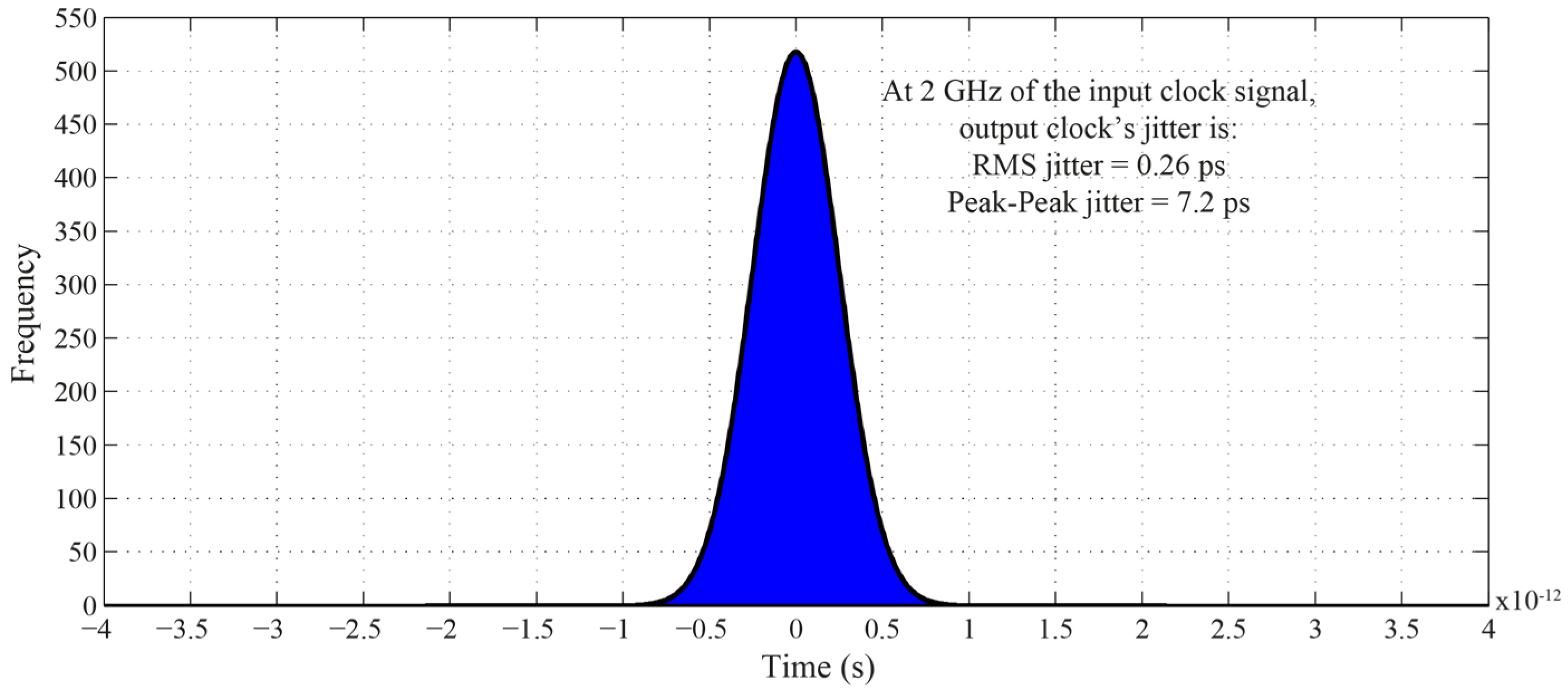
Simulation results on jitter show that the output jitter of the DLL is remarkably low.
Figure 12 shows the simulated jitter when the DLL is operated at 2 GHz of the input reference signal. The peak-to-peak and RMS values are 7.2 ps and 0.26 ps, respectively. As mentioned, this is attributed to the cycle-to-cycle reset operation of the charge pump’s capacitor, which significantly minimizes the accumulated noise originated from the charge pump’s amplifier. It is also worth mentioning that the low jitter is attributed to the use of only one NAND gate-based buffer in the VCDL circuit.
In addition, the effects of the PVT variations on the jitter performance have also been simulated and analyzed, as shown in
Figure 13.
Since the desired value of the output jitter is in the sub-picosecond range, it can be noted in
Figure 13a that only the process corner FS degrades the jitter. However, this shortcoming can be mitigated by optimizing the pulse width of the reset pulse, ϕ
R. In
Figure 13b, only two temperature and supply voltage variations located at 1.02 V for 0 °C and 27 °C, which are dark black-colored and dark grey-colored, can degrade the output jitter to over 1.75 ps RMS and 1.3 ps RMS, respectively.
A summary of the performance specifications and results of the proposed work is presented in
Table 2. The proposed CRC technique successfully achieves sub-picosecond-resolution delay step, a high number of delay steps within a specific range, sub-picosecond jitter performance, a wide operating frequency range, sub-milliwatt power consumption, and a small occupied active area for layout. The layout area is significantly minimized because the VCDL, which is followed by an uncontrolled inverter-based buffer as shown in
Figure 1a, only uses a single NAND-based buffer. It is worth mentioning that the achieved delay range for the case without the proposed CRC technique is only 2 ps using the same transistor sizes and operating conditions as in the case with the CRC whose achieved delay range is 69 ps.
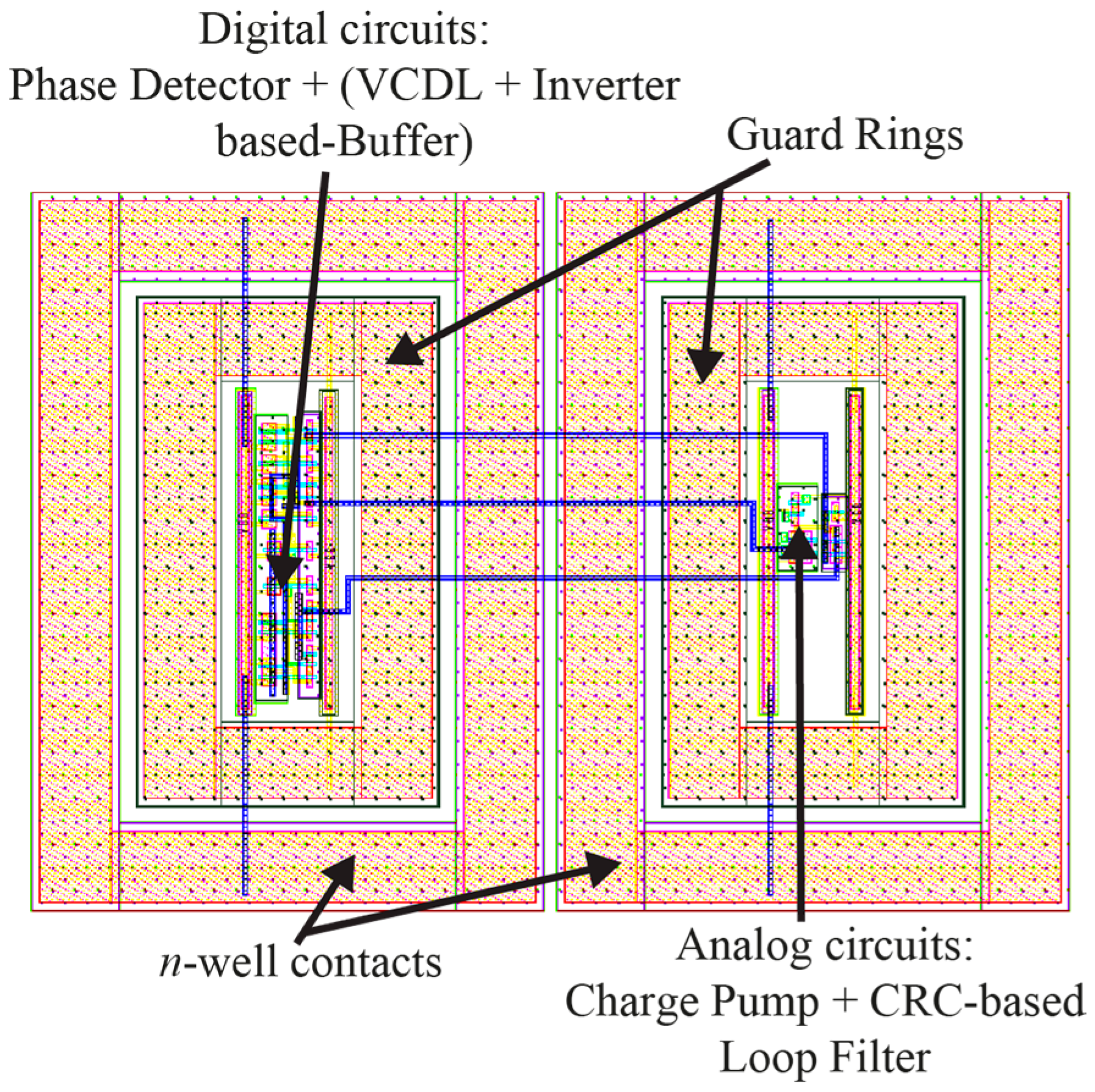
The layout of the proposed DLL circuit architecture is shown in
Figure 14.
It can be seen in
Figure 14 that guard rings and
n-well contacts have been used for the proposed DLL’s layout in order to reduce the effects of the substrate and power noise. In addition, separation of the digital circuits from the analog circuits as well as utilizing separate VDD and GND lines for each of these circuits have been employed to further reduce the substrate noise effects.
In order to compare the performance of this work with other reported high-resolution DLL circuits,
Table 3 is presented. In this table, the proposed work has been compared with the work reported by [
12], which has been presented earlier in
Table 1 and has shown to have almost the best performance compared with the other works in
Table 1.
According to
Table 3, the proposed lock-range extension technique in this work achieves higher-resolution delay step, higher number of delay steps within a specific range, better jitter performance, lower power consumption, and smaller occupied active area.


