
A Selective Change Driven System for High-Speed Motion Analysis


Abstract
:1. Introduction
1.1. Event-Based Sensors
1.2. Event-Based Systems
1.3. Laser Scanning
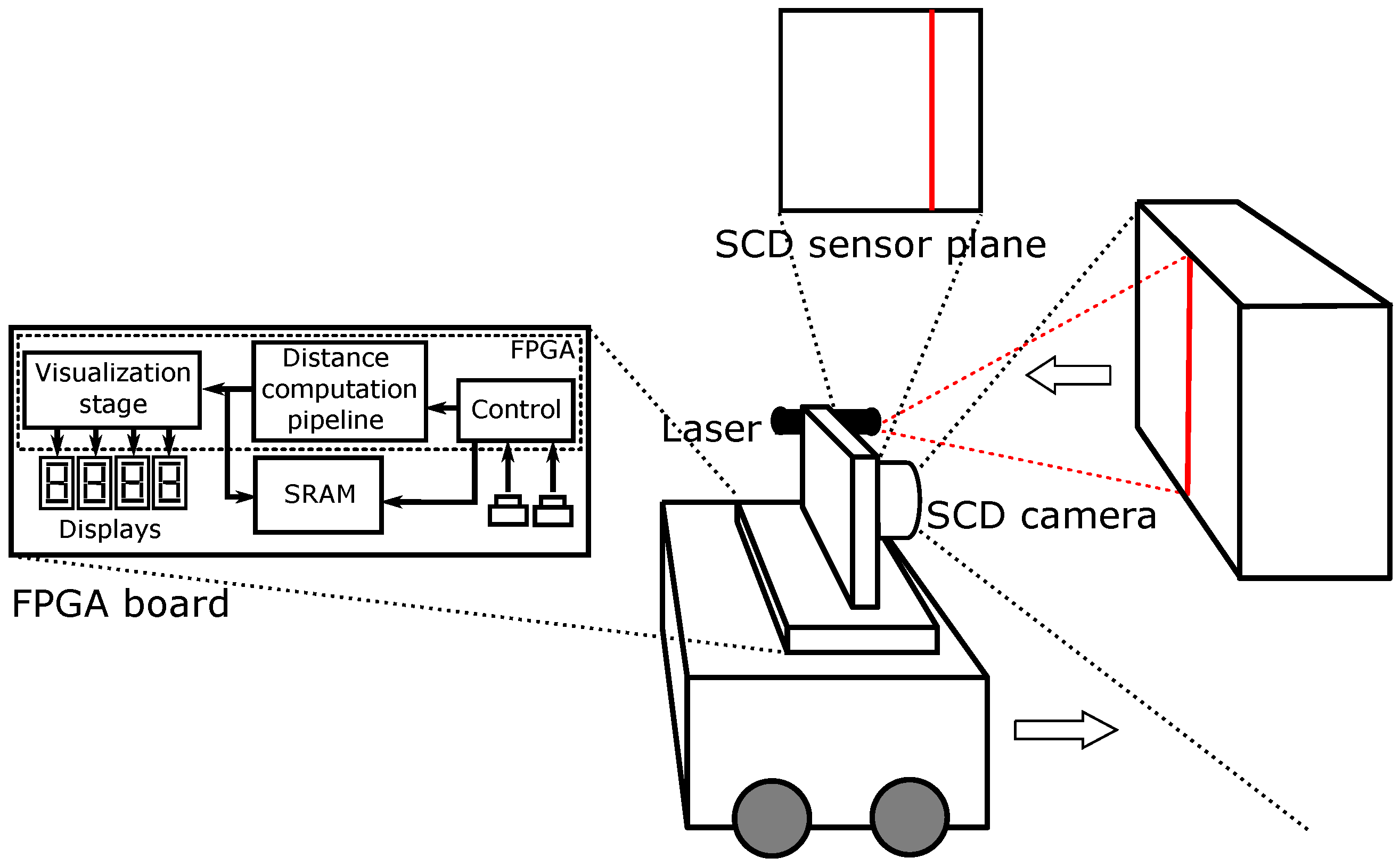
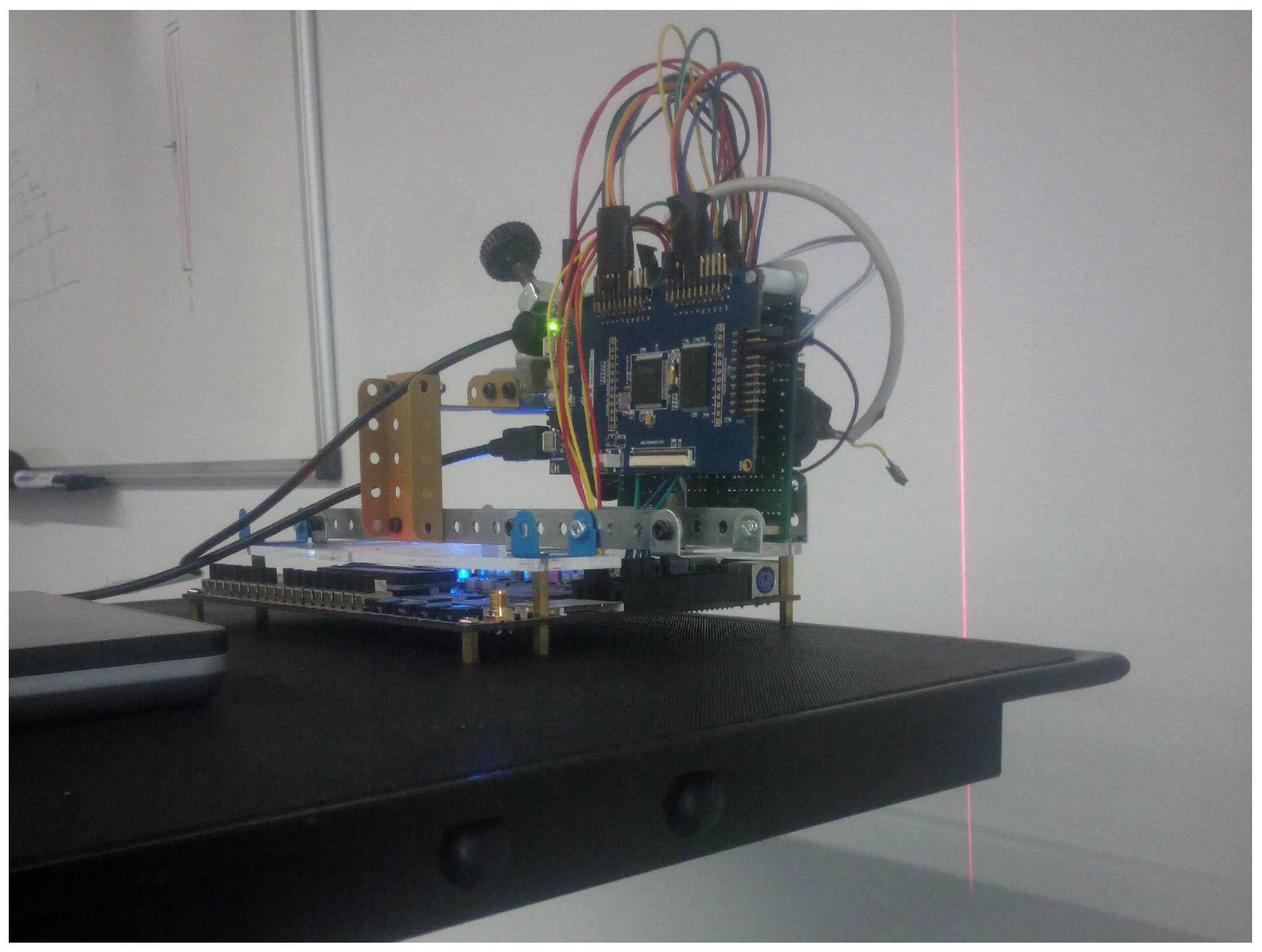
2. System Description
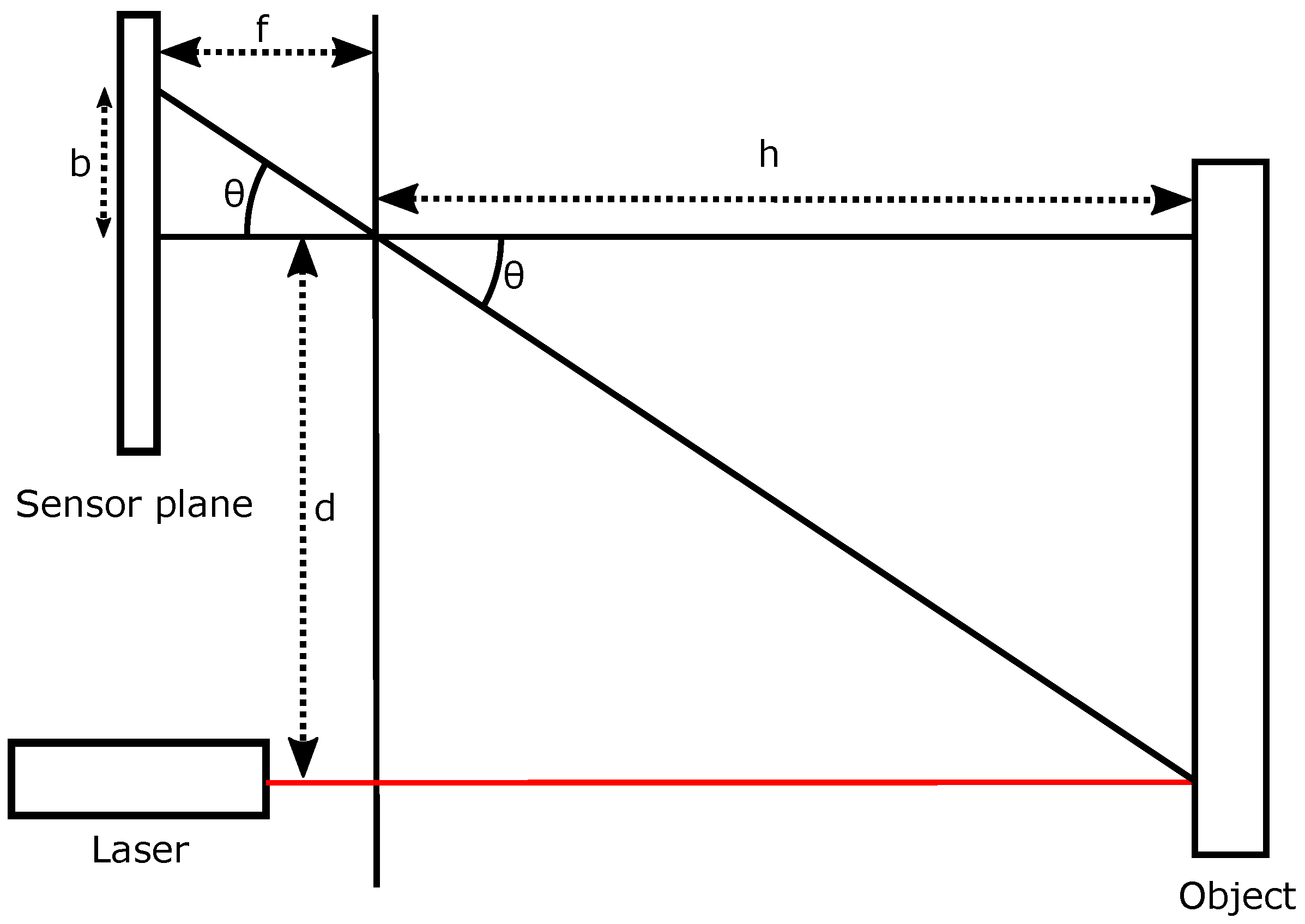
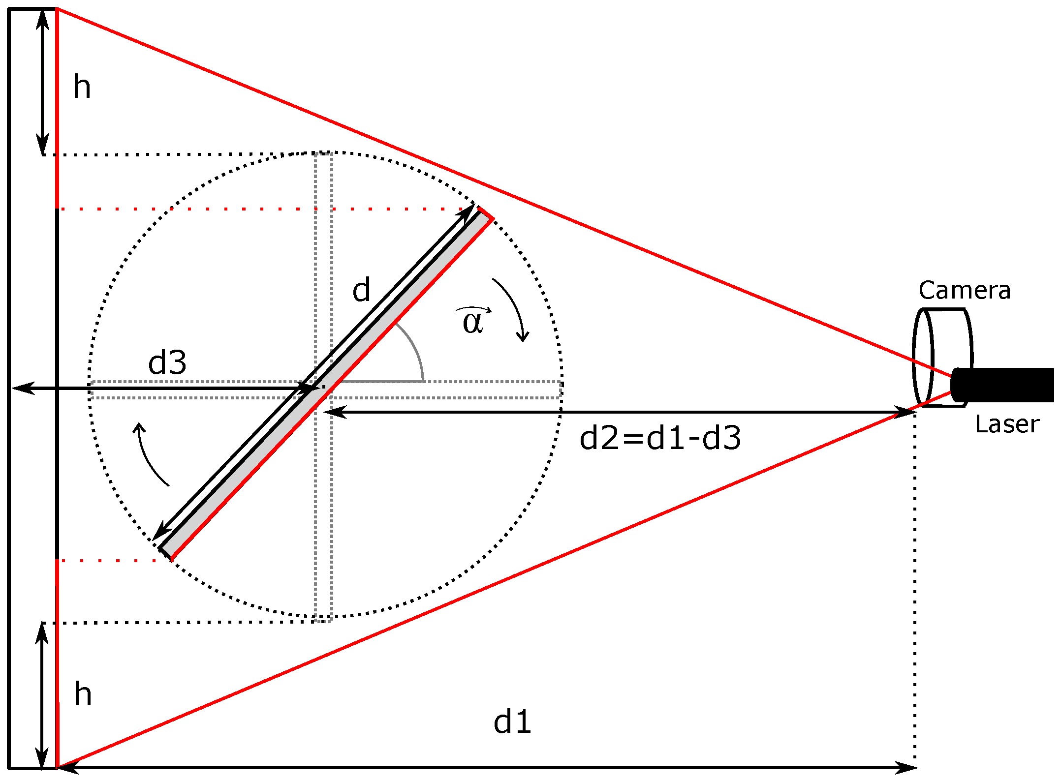
2.1. Laser Triangulation System
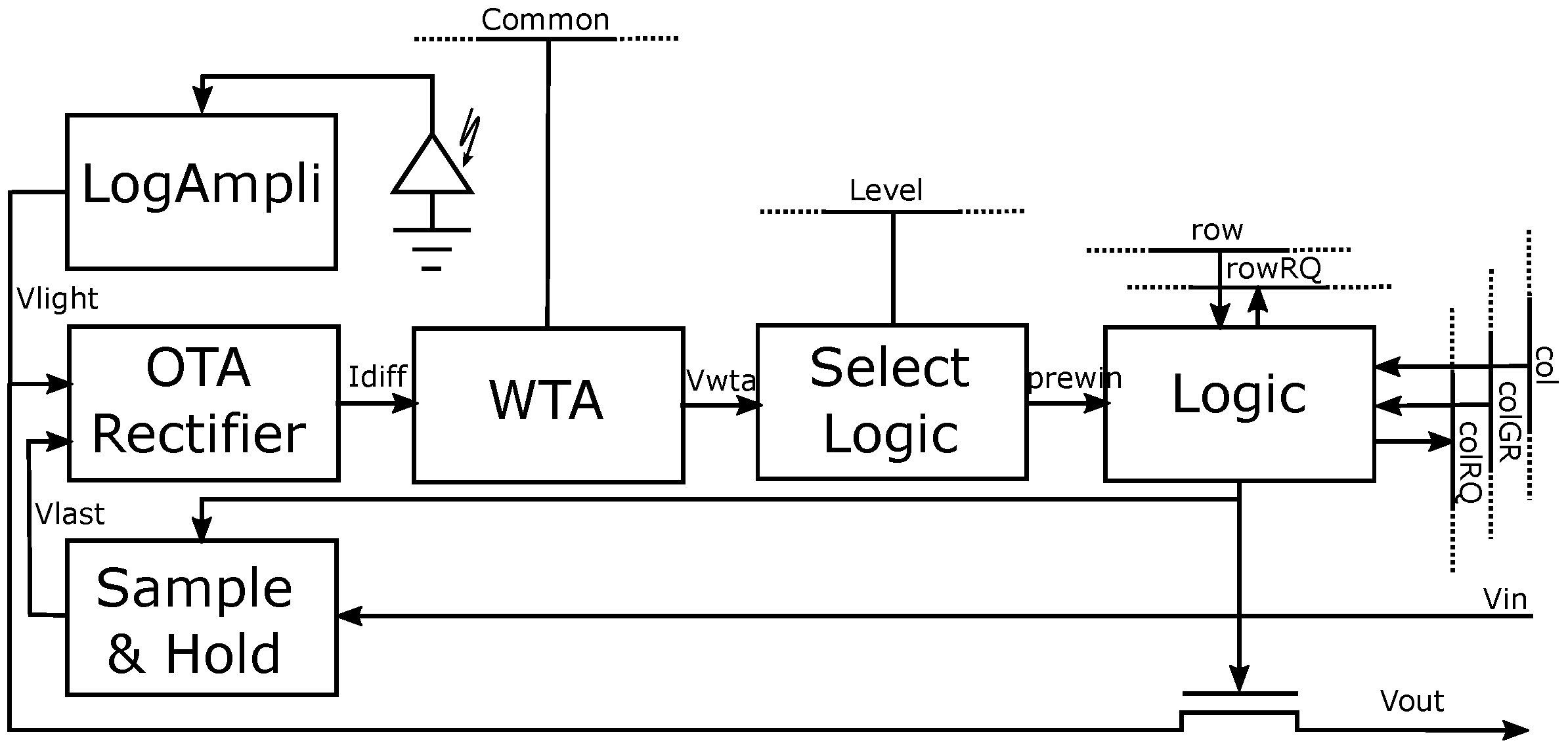
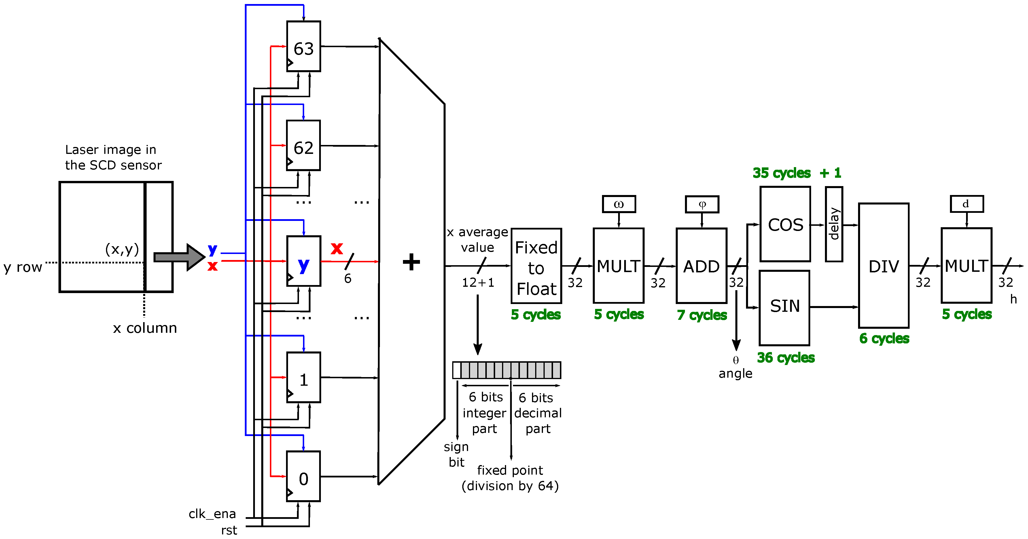
2.2. SCD Sensor
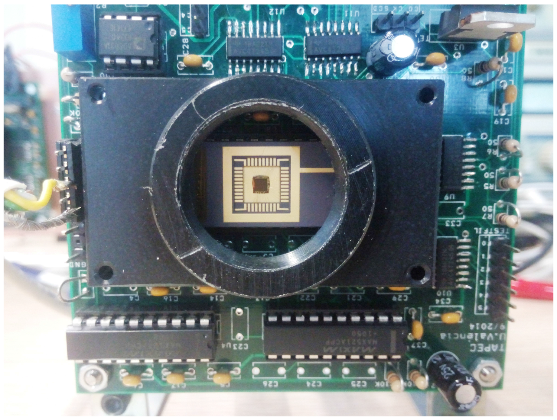
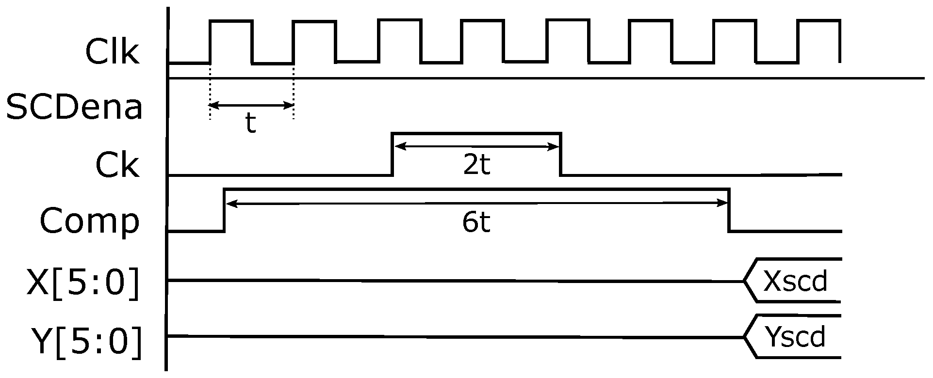
2.3. SCD Camera
2.4. High-Speed Computation Pipeline
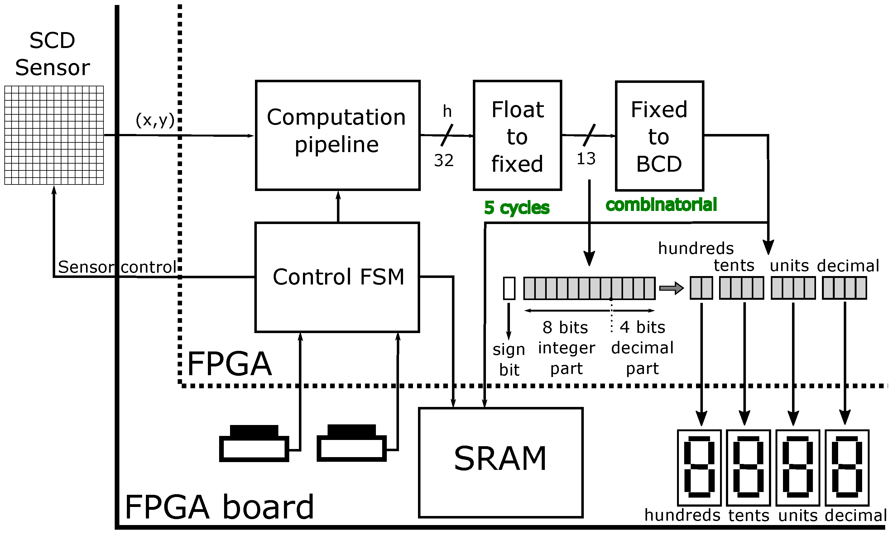
2.5. Display Stage and Memory Access
2.6. Synthesis Details
- 33,216 logic elements
- 105 M4K RAM (Random Access Memory) blocks
- 483,840 total RAM bits
- 35 embedded multipliers
- 4 PLLs (Phase-Locked Loops)
- 475 user I/O pins
- FineLine BGA (Ball Grid Array) 672-pin package.
3. Experimentation
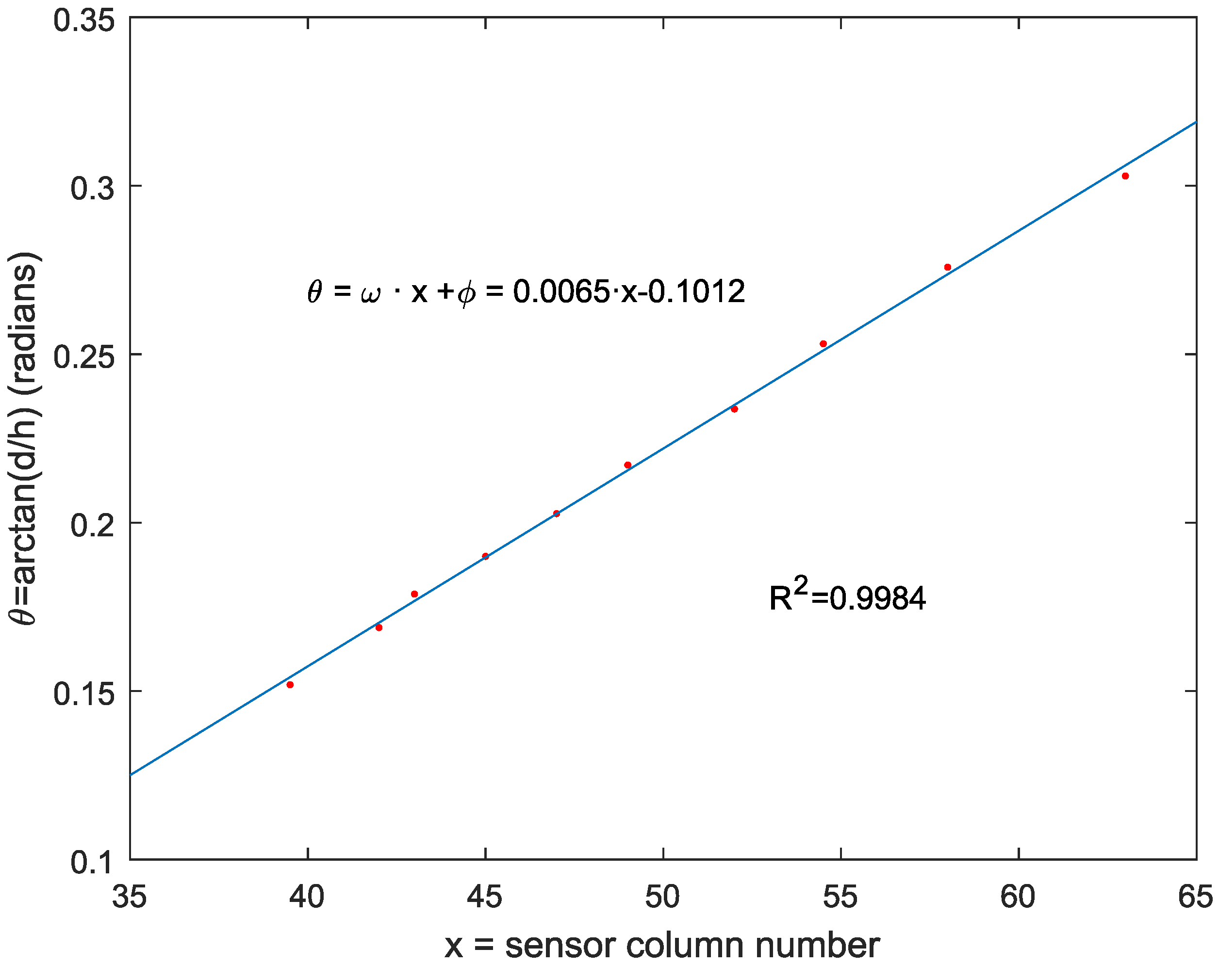
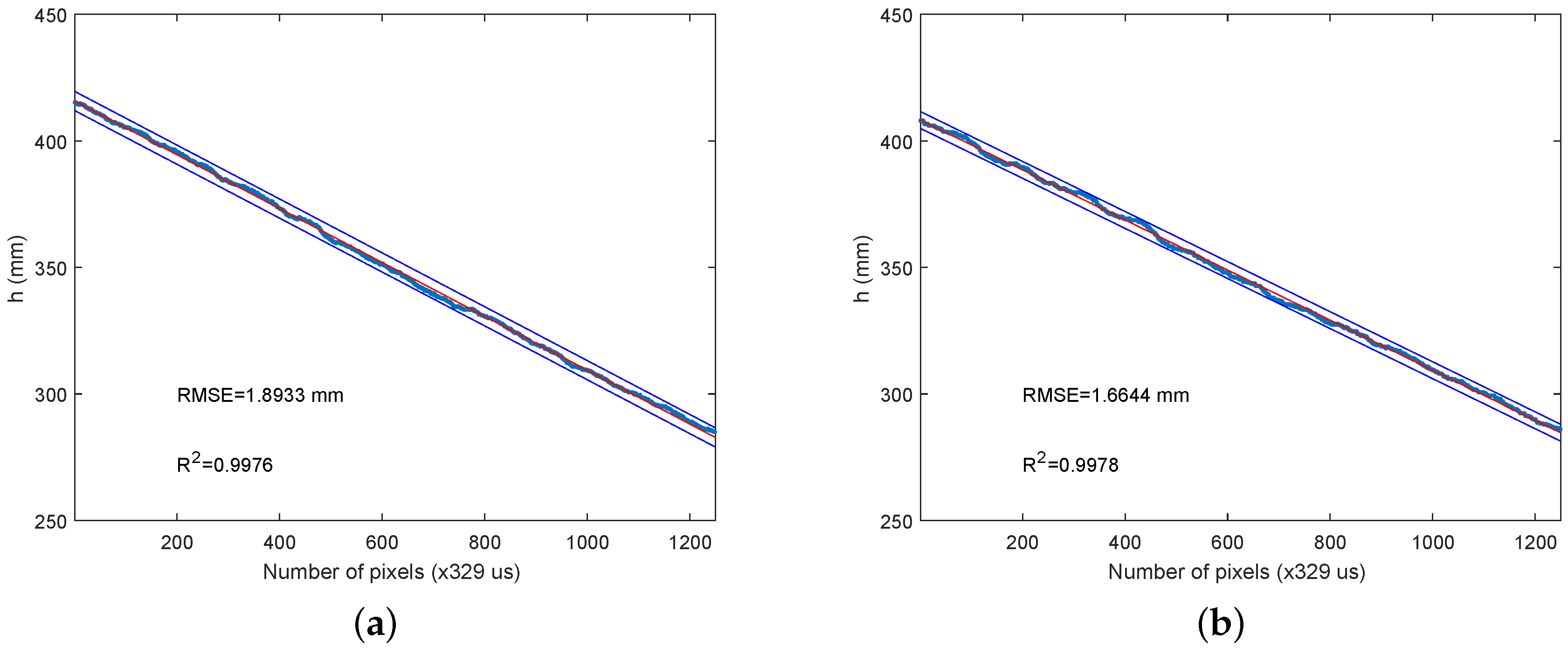
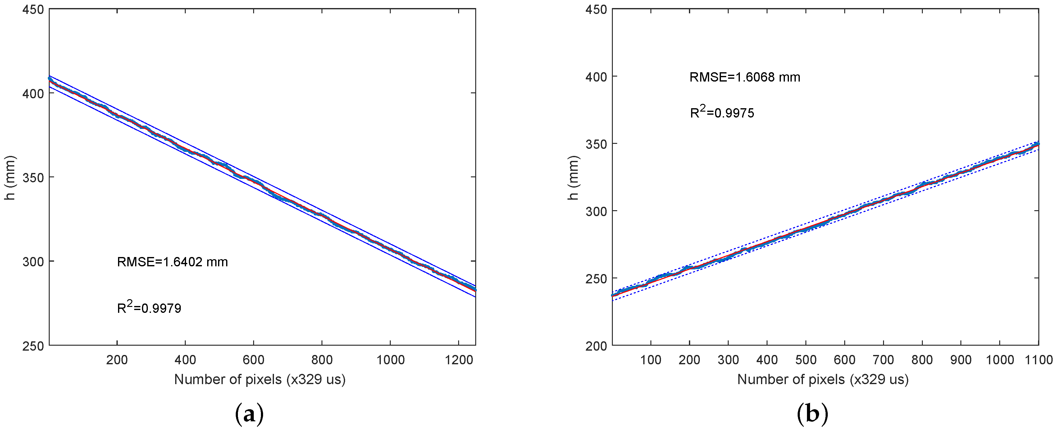
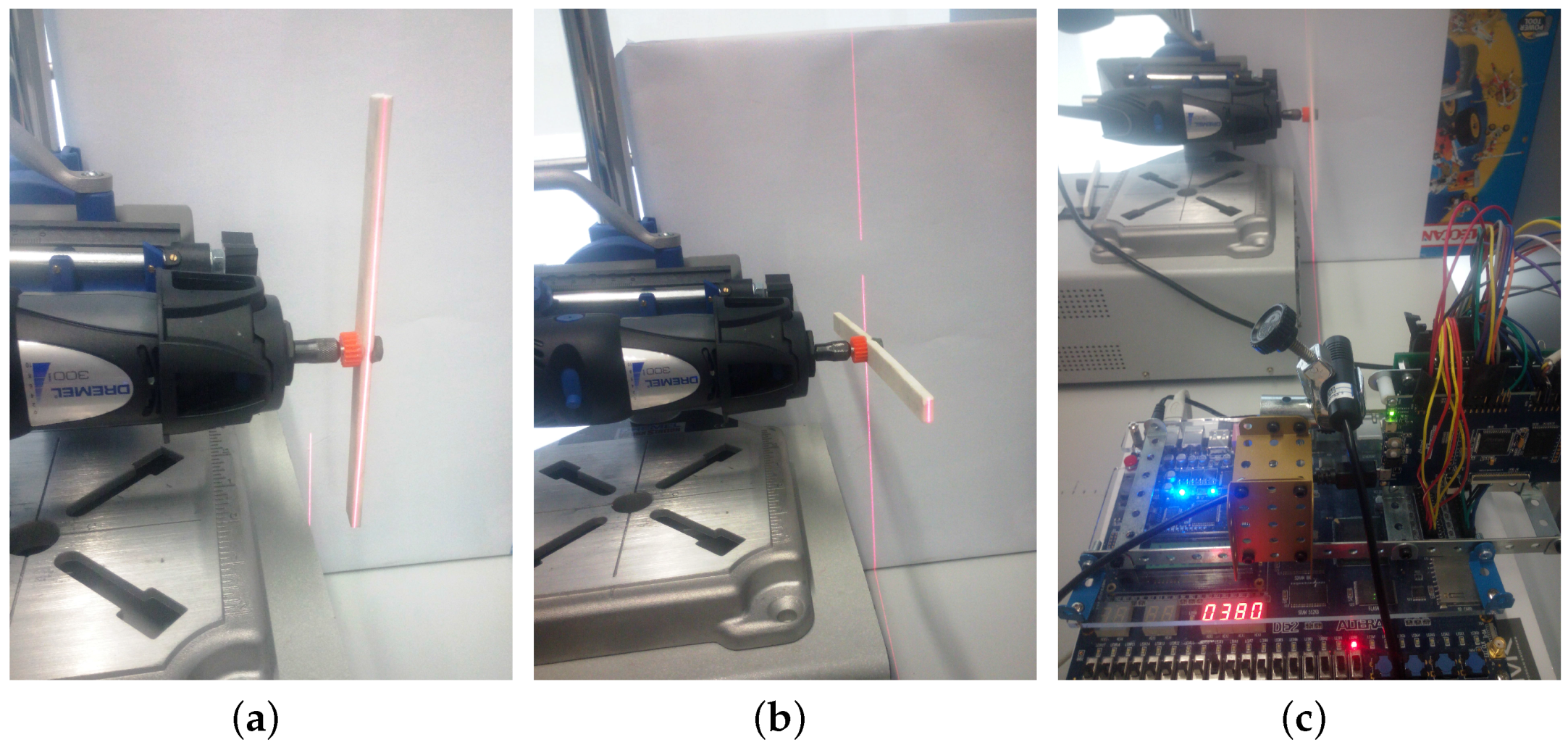
3.1. Calibration
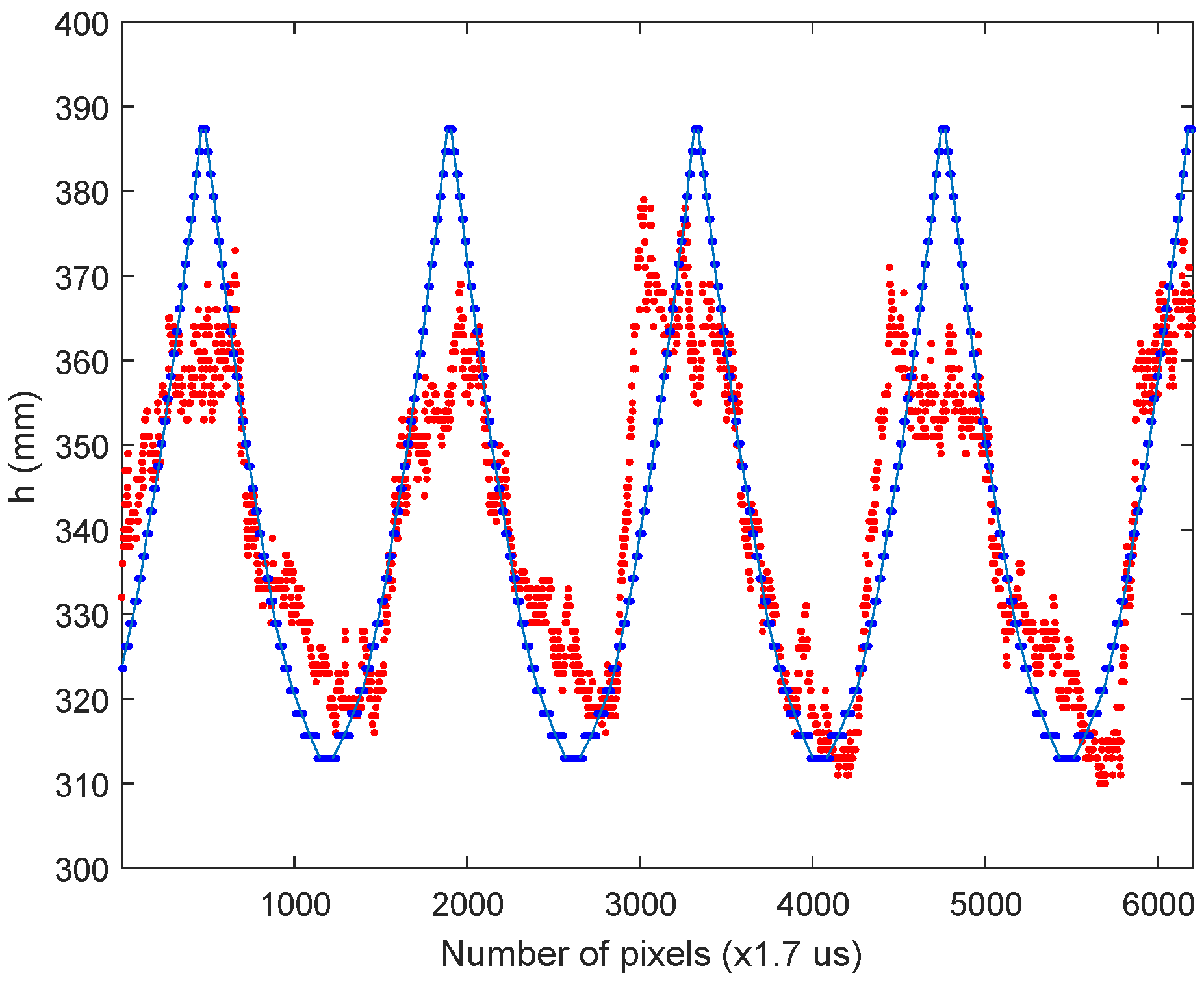
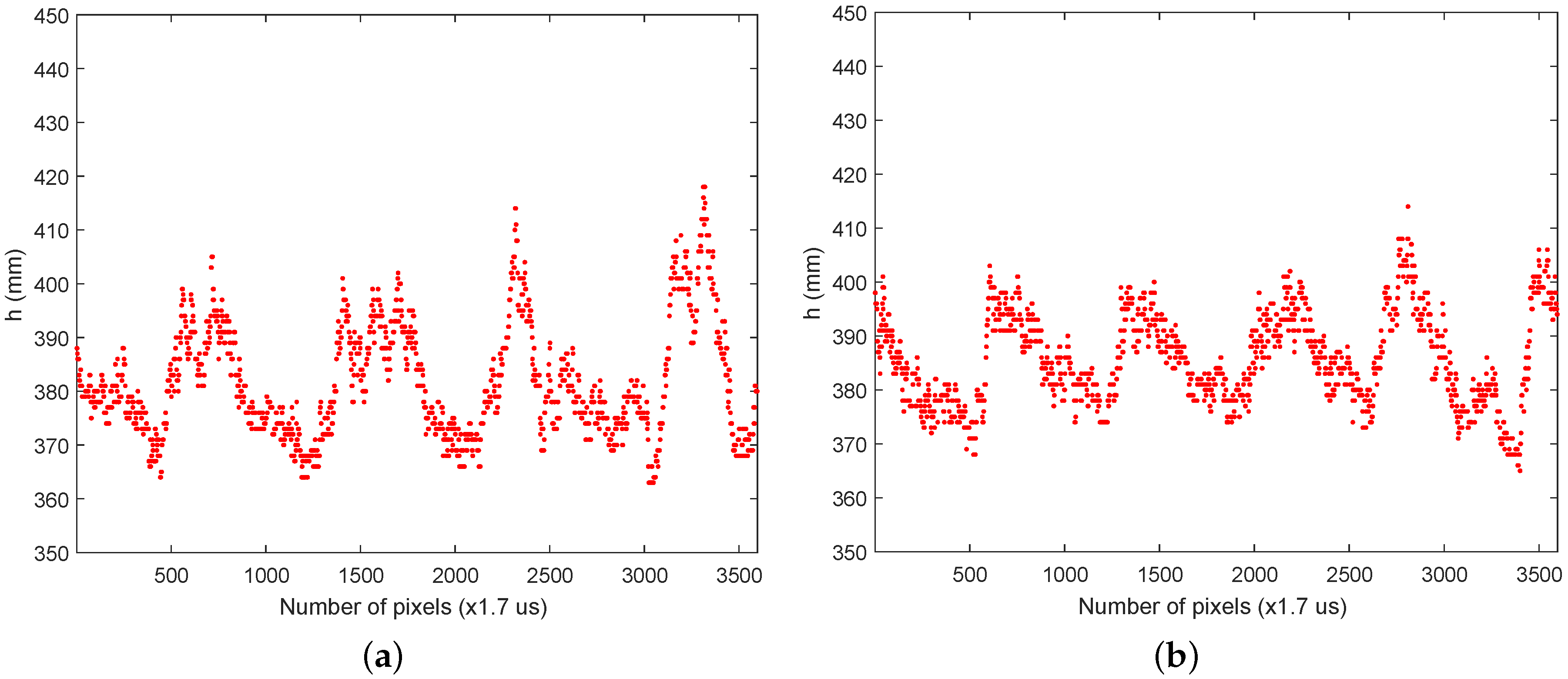
3.2. High-Speed Experiments
4. Conclusions
Acknowledgments
Author Contributions
Conflicts of Interest
Abbreviations
| AER | Address Event Representation |
| CK | Clock sensor signal |
| CMOS | Complementary Metal Oxide Semiconductor |
| Comp | Competition sensor signal |
| ConvNets | Convolutional Neural Networks |
| DVS | Dynamic Vision Sensor |
| FPGA | Field Programmable Gate Array |
| fps | frames per second |
| FSM | Finite State Machine |
| Kfps | Kilo frames per second |
| LiDAR | Light Detection and Ranging or Laser Imaging Detection and Ranging |
| LPM | Library of Parameterized Modules |
| LUT | Look-Up Table |
| PLD | Programmable Logic Device |
| RMSE | Root Mean Square Error |
| RTS | Random Telegraph Signal |
| SCD | Selective Change-Driven |
| SRAM | Static Random Access Memory |
| ToF | Time of Flight |
| VLSI | Very Large Scale of Integration |
| WTA | Winner-Take-All |
References
- Cha, Y.J.; You, K.; Choi, W. Vision-Based Detection of Loosened Bolts using the Hough Transform and Support Vector Machines. Autom. Constr. 2016, 71, 181–188. [Google Scholar] [CrossRef]
- Vincent, J.F.V. Biomimetics—A Review. Proc. Inst. Mech. Eng. Part H 2009, 223, 919–939. [Google Scholar] [CrossRef]
- Antonietti, A.; Casellato, C.; Garrido, J.A.; Luque, N.R.; Naveros, F.; Ros, E.; D’Angelo, E.; Pedrocchi, A. Spiking Neural Network with Distributed Plasticity Reproduces Cerebellar Learning in Eye Blink Conditioning Paradigms. IEEE Trans. Biomed. Eng. 2016, 63, 210–219. [Google Scholar] [CrossRef] [PubMed]
- Gollisch, T.; Meister, M. Rapid Neural Coding in the Retina with Relative Spike Latencies. Science 2008, 319, 1108–1111. [Google Scholar] [CrossRef] [PubMed]
- Pardo, F.; Benavent, X.; Boluda, J.A.; Vegara, F. Selective Change-Driven Image Processing for High-Speed Motion estimation. In Proceedings of the 13th International Conference on Systems, Signals and Image Processing (IWSSIP), Budapest, Hungary, 21–23 September 2006; pp. 163–166.
- Mahowald, M. VLSI Analogs of Neural Visual Processing: A Synthesis of Form and Function. Ph.D. Thesis, Computer Science Divivision, California Institute of Technology, Pasadena, CA, USA, 1992. [Google Scholar]
- Vanarse, A.; Osseiran, A.; Rassau, A. A Review of Current Neuromorphic Approaches for Vision, Auditory, and Olfactory Sensors. Front. Neurosci. 2016, 10, 115. [Google Scholar] [CrossRef] [PubMed]
- Kim, D.; Culurciello, E. Tri-Mode Smart Vision Sensor With 11-Transistors/Pixel for Wireless Sensor Networks. IEEE Sens. J. 2013, 13, 2102–2108. [Google Scholar] [CrossRef]
- Posch, C.; Matolin, D.; Wohlgenannt, R. A QVGA 143 dB Dynamic Range Frame-Free PWM Image Sensor with Lossless Pixel-Level Video Compression and Time-Domain CDS. IEEE J. Solid State Circuits 2011, 46, 259–275. [Google Scholar] [CrossRef]
- Brandli, C.; Berner, R.; Yang, M.; Liu, S.C.; Delbruck, T. A 240 × 180 130 dB 3 μs Latency Global Shutter Spatiotemporal Vision Sensor. IEEE J. Solid State Circuits 2014, 49, 2333–2341. [Google Scholar] [CrossRef]
- Serrano-Gotarredona, T.; Linares-Barranco, B. A 128 × 128 1.5% Contrast Sensitivity 0.9% FPN 3 μs Latency 4 mW Asynchronous Frame-Free Dynamic Vision Sensor Using Transimpedance Preamplifiers. IEEE J. Solid State Circuits 2013, 48, 827–838. [Google Scholar] [CrossRef]
- Lichtsteiner, P.; Posch, C.; Delbruck, T. A 128 × 128 dB 15 μs Latency Asynchronous Temporal Contrast Vision Sensor. IEEE J. Solid State Circuits 2008, 43, 566–576. [Google Scholar] [CrossRef] [Green Version]
- Pardo, F.; Boluda, J.A.; Vegara, F. Selective Change Driven Vision Sensor with Continuous-Time Logarithmic Photoreceptor and Winner-Take-All Circuit for Pixel Selection. IEEE J. Solid State Circuits 2015, 50, 786–798. [Google Scholar] [CrossRef]
- Zuccarello, P.; Pardo, F.; de la Plaza, A.; Boluda, J.A. 32 × 32 Winner-Take-All matrix with single winner selection. Electron. Lett. 2010, 46, 333–335. [Google Scholar] [CrossRef]
- Herculano-Houzel, S. The Human Brain in Numbers: A Linearly Scaled-up Primate Brain. Front. Hum. Neurosci. 2009, 3, 31. [Google Scholar] [CrossRef] [PubMed]
- van Schaik, A.; Delbruck, T.; Hasler, J. Neuromorphic Engineering Systems and Applications; Frontiers in Neuroscience, Frontiers Media: Lausanne, Switzerland, 2015. [Google Scholar]
- Liu, S.C.; Delbruck, T.; Indiveri, G.; Whatley, A.; Douglas, R. Event-Based Neuromorphic Systems; John Wiley & Sons Ltd.: Chichester, UK, 2015. [Google Scholar]
- Ramos, C.Z. Modular and Scalable Implementation of AER Neuromorphic Systems. Ph.D. Thesis, Universidad de Sevilla, Sevilla, Spain, 2011. [Google Scholar]
- Camunas-Mesa, L.; Zamarreno-Ramos, C.; Linares-Barranco, A.; Acosta-Jimenez, A.J.; Serrano-Gotarredona, T.; Linares-Barranco, B. An Event-Driven Multi-Kernel Convolution Processor Module for Event-Driven Vision Sensors. IEEE J. Solid State Circuits 2012, 47, 504–517. [Google Scholar] [CrossRef]
- Camunas-Mesa, L.A.; Serrano-Gotarredona, T.; Linares-Barranco, B. Event-Driven Sensing and Processing for High-Speed Robotic Vision. In Proceedings of the IEEE Biomedical Circuits and Systems Conference (BioCAS), Lausanne, Switzerland, 22–24 October 2014; pp. 516–519.
- Yousefzadeh, A.; Serrano-Gotarredona, T.; Linares-Barranco, B. Fast Pipeline 128 ×128 pixel Spiking Convolution Core for Event-Driven Vision Processing in FPGAs. In Proceedings of the First IEEE International Conference on Event-based Control, Communication, and Signal Processing (EBCCSP), Krakow, Poland, 17–19 June 2015; pp. 1–8.
- Budzan, S.; Kasprzyk, J. Fusion of 3D Laser Scanner and Depth Images for Obstacle Recognition in Mobile Applications. Opt. Laser Eng. 2016, 77, 230–240. [Google Scholar] [CrossRef]
- Guana, H.; Libc, J.; Caoa, S.; Yud, Y. Use of Mobile LiDAR in Road Information Inventory: A Review. Int. J. Image Data Fusion 2016, 7, 219–242. [Google Scholar] [CrossRef]
- Clarke, T.; Grattan, K.; Lindsey, N. Laser-based Triangularion Techniques in Optical Inspection of Industrial Structures. Proc. SPIE 1990, 1332, 474–486. [Google Scholar]
- Khademi, S.; Darudi, A.; Abbasi, Z. A Sub Pixel Resolution Method. World Acad. Sci. Eng. Technol. 2010, 70, 578–581. [Google Scholar]
- Peiravi, A.; Taabbodi, B. A Reliable 3D Laser Triangulation-based Scanner with a New Simple but Accurate Procedure for Finding Scanner Parameters. J. Am. Sci. 2010, 6, 80–85. [Google Scholar]
- Kneip, L.; Tache, F.; Caprari, G.; Siegwart, R. Characterization of the Compact Hokuyo URG-04LX 2D Laser Range Scanner. In Proceedings of the IEEE International Conference on Robotics and Automation (ICRA), Kobe, Japan, 12–17 May 2009; pp. 2522–2529.
- Foix, S.; Alenya, G.; Torras, C. Lock-in Time-of-Flight (ToF) Cameras: A Survey. IEEE Sens. J. 2011, 11, 1917–1926. [Google Scholar] [CrossRef] [Green Version]
- Khoshelham, K.; Elberink, S.O. Accuracy and Resolution of Kinect Depth Data for Indoor Mapping Applications. Sensors 2012, 12, 1437–1454. [Google Scholar] [CrossRef] [PubMed]
- Chen, J.G.; Wadhwa, N.; Cha, Y.J.; Durand, F.; Freeman, W.T.; Buyukozturk, O. Modal Identification of Simple Structures with High-Speed Video using Motion Magnification. J. Sound Vib. 2015, 345, 58–71. [Google Scholar] [CrossRef]
- Cha, Y.J.; Chen, J.G.; Buyukozturk, O. Motion Magnification Based Damage Detection Using High Speed Video. In Proceedings of the 10th International Workshop On Structural Health Monitoring (IWSHM), Stanford, CA, USA, 1–3 September 2015.
- Vegara, F.; Zuccarello, P.; Boluda, J.A.; Pardo, F. Taking Advantage of Selective Change Driven Processing for 3D Scanning. Sensors 2013, 13, 13143–13162. [Google Scholar] [CrossRef] [PubMed]
- Acosta, D.; Garcia, O.; Aponte, J. LaserTriangulation for Shape Acquisition in a 3D Scanner Plus Scanner. In Proceedings of the Electronics, Robotics and Automotive Mechanics Conference (CERMA), Cuernavaca, Mexico, 26–29 September 2006; pp. 14–19.
- Zuccarello, P.; Pardo, F.; de la Plaza, A.; Boluda, J.A. A 32 × 32 Pixels Vision Sensor for Selective Change Driven Readout Strategy. In Proceedings of the 36th European Solid State Circuits Conference (ESSCIRC), Sevilla, Spain, 14–16 September 2010.
- Pardo, F.; Zuccarello, P.; Boluda, J.A.; Vegara, F. Advantages of Selective Change Driven Vision for Resource-Limited Systems. IEEE Trans. Circuits Syst. Video 2011, 21, 1415–1423. [Google Scholar] [CrossRef]
- Kiran, R.; Nampally, S. Analyzing the Performance of Carry Tree Adders Based on FPGA’s. Int. J. Electron. Signals Syst. 2012, 2, 54–58. [Google Scholar]
- Pardo, F.; Boluda, J.A.; Vegara, F. Random Telegraph Signal Transients in Active Logarithmic Continuous-Time Vision Sensors. Solid State Electron. 2015, 114, 111–114. [Google Scholar] [CrossRef]


| Parameter | Value |
|---|---|
| System clock | 97.84 MHz |
| Total logic elements | 16,064 (48%) |
| Total registers | 8285 (25%) |
| Total memory bits | 4608 (1%) |
| Embedded Multiplier 9-bit elements | 70 (100%) |
© 2016 by the authors; licensee MDPI, Basel, Switzerland. This article is an open access article distributed under the terms and conditions of the Creative Commons Attribution (CC-BY) license (http://creativecommons.org/licenses/by/4.0/).
Share and Cite
Boluda, J.A.; Pardo, F.; Vegara, F. A Selective Change Driven System for High-Speed Motion Analysis. Sensors 2016, 16, 1875. https://0-doi-org.brum.beds.ac.uk/10.3390/s16111875
Boluda JA, Pardo F, Vegara F. A Selective Change Driven System for High-Speed Motion Analysis. Sensors. 2016; 16(11):1875. https://0-doi-org.brum.beds.ac.uk/10.3390/s16111875
Chicago/Turabian StyleBoluda, Jose A., Fernando Pardo, and Francisco Vegara. 2016. "A Selective Change Driven System for High-Speed Motion Analysis" Sensors 16, no. 11: 1875. https://0-doi-org.brum.beds.ac.uk/10.3390/s16111875