
Theoretical Design of a Depolarized Interferometric Fiber-Optic Gyroscope (IFOG) on SMF-28 Single-Mode Standard Optical Fiber Based on Closed-Loop Sinusoidal Phase Modulation with Serrodyne Feedback Phase Modulation Using Simulation Tools for Tactical and Industrial Grade Applications


Abstract
:
1. Introduction
2. Sensor Design
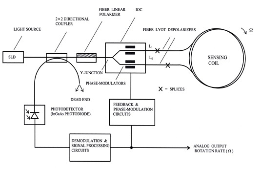
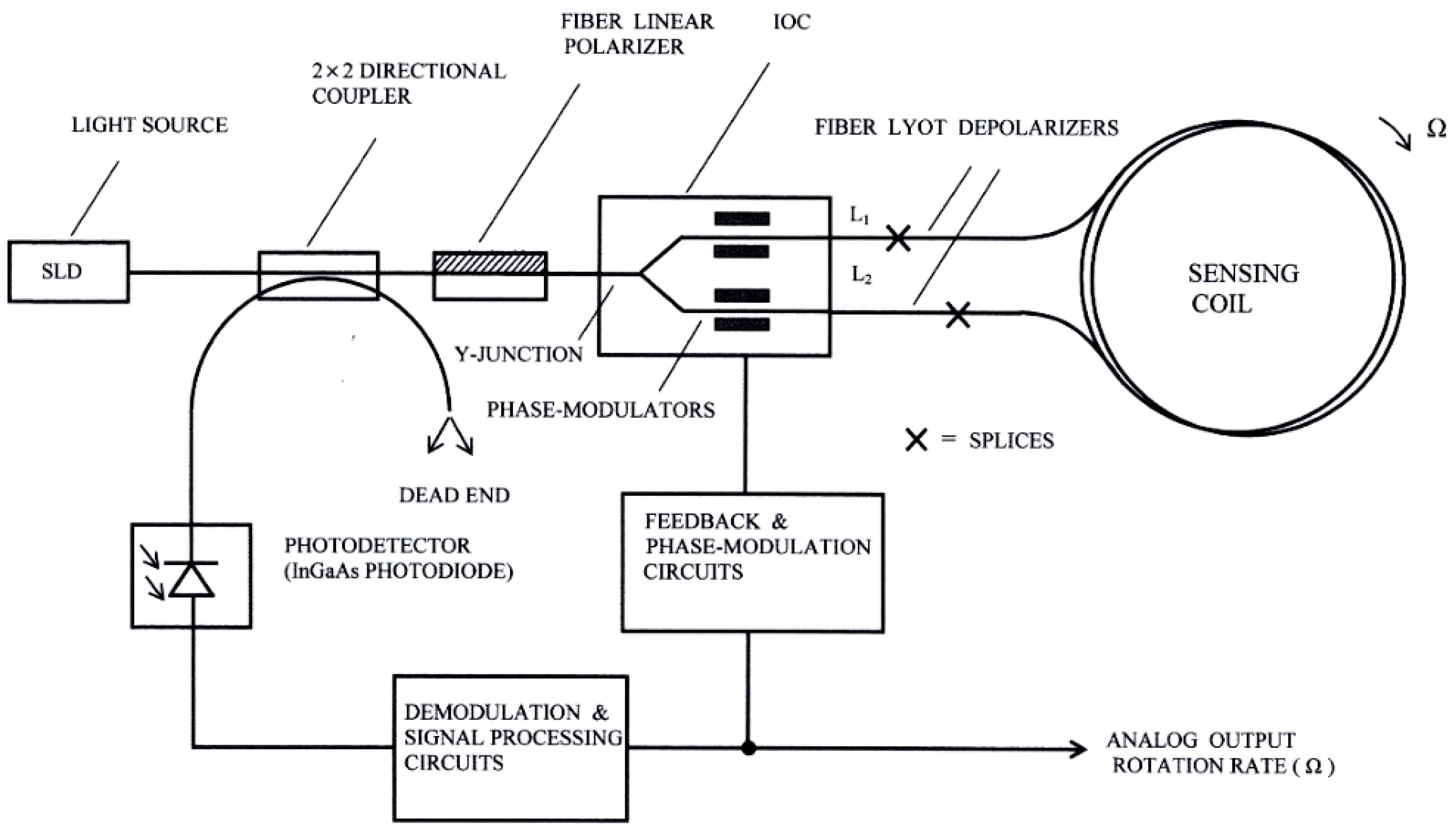
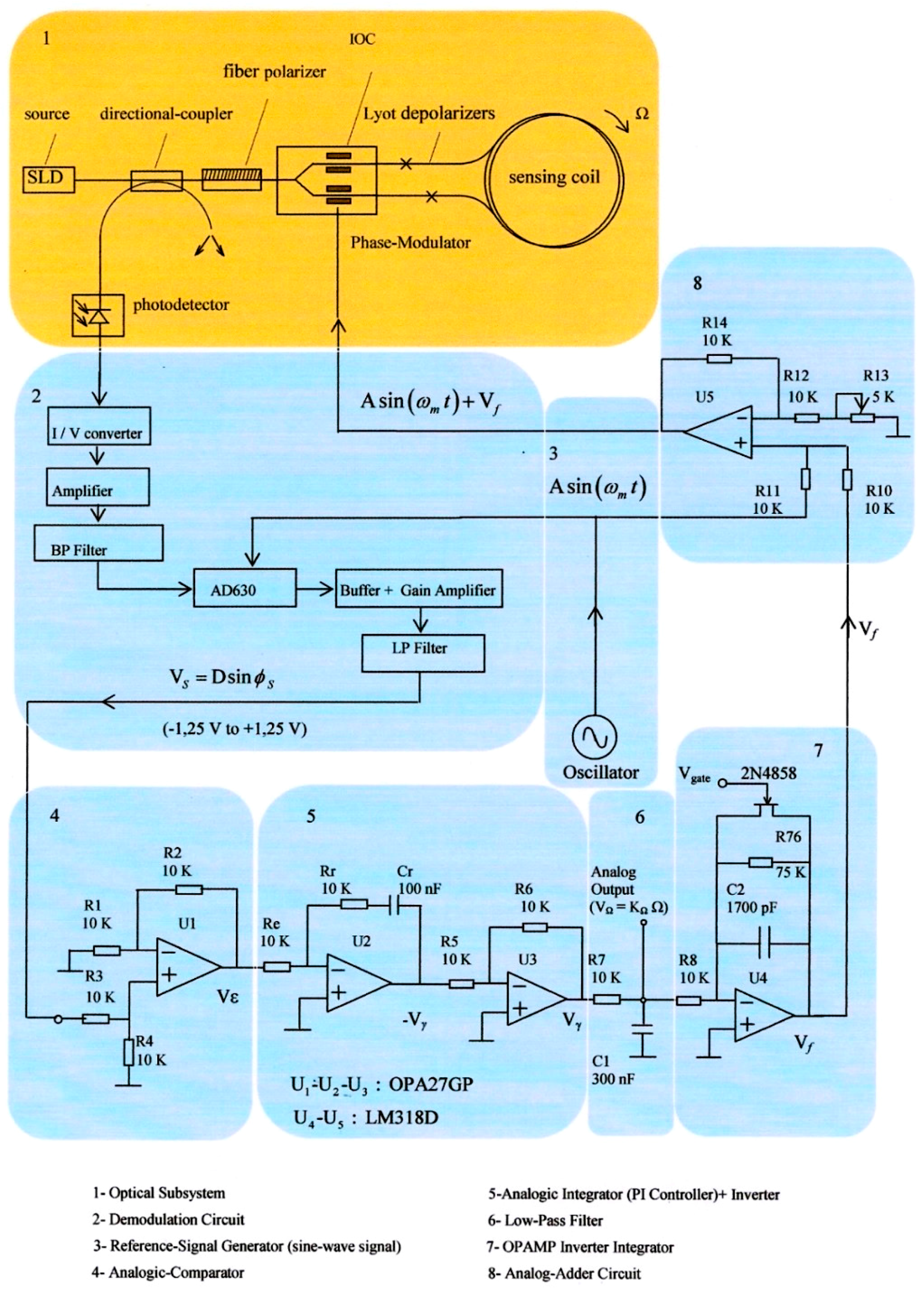
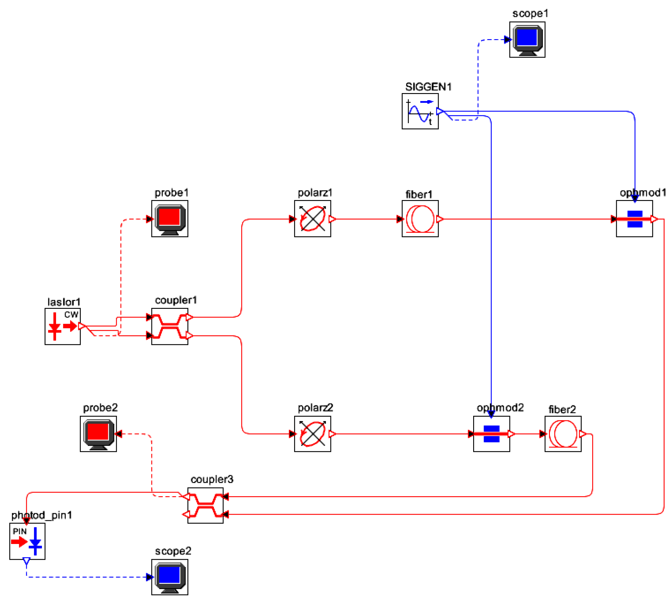
2.1. Design of the Optical System
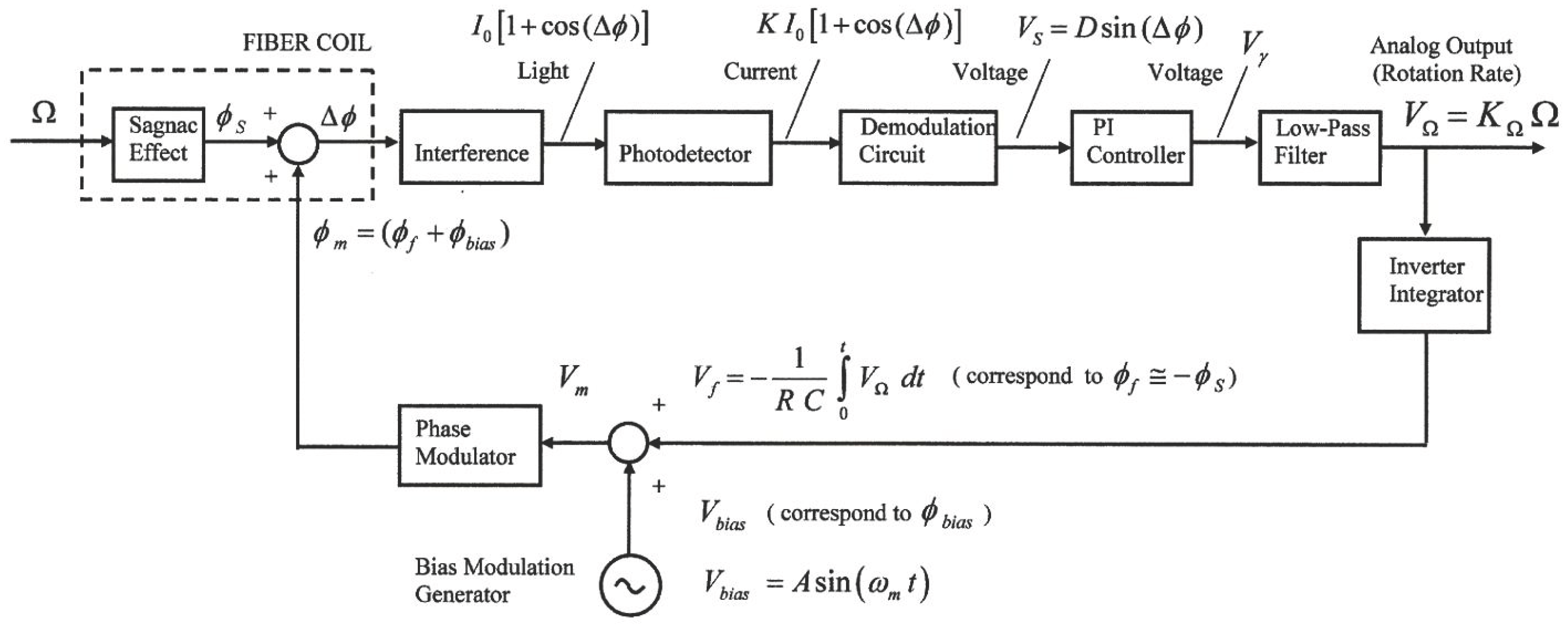
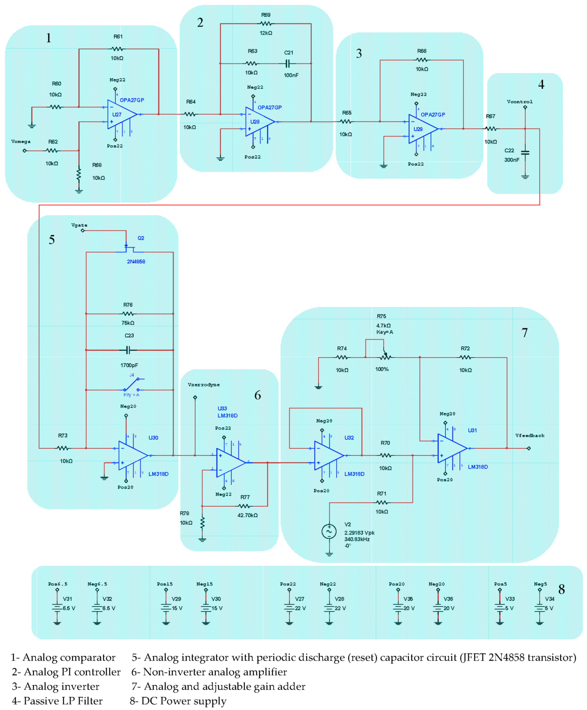
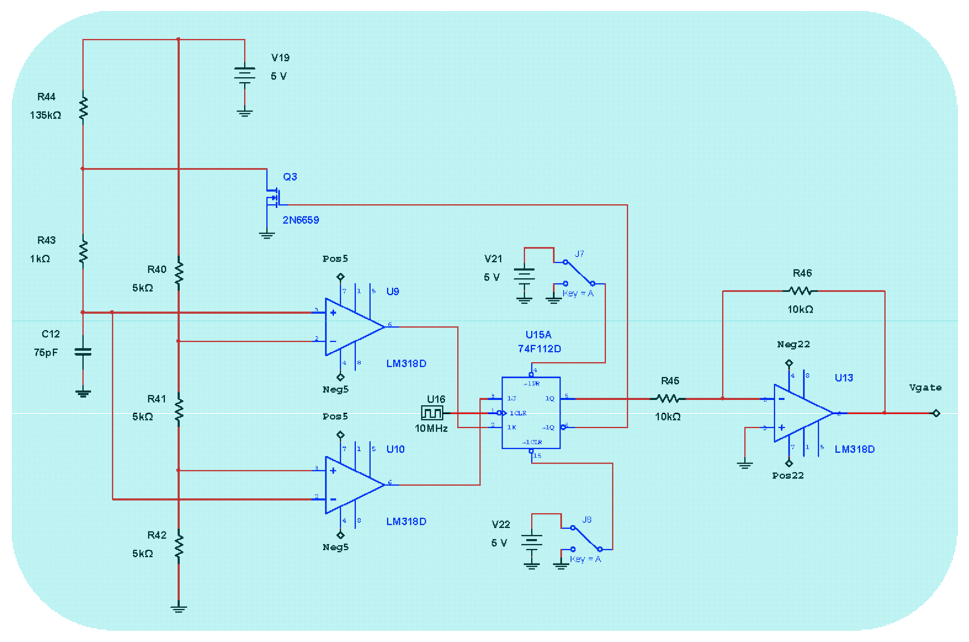
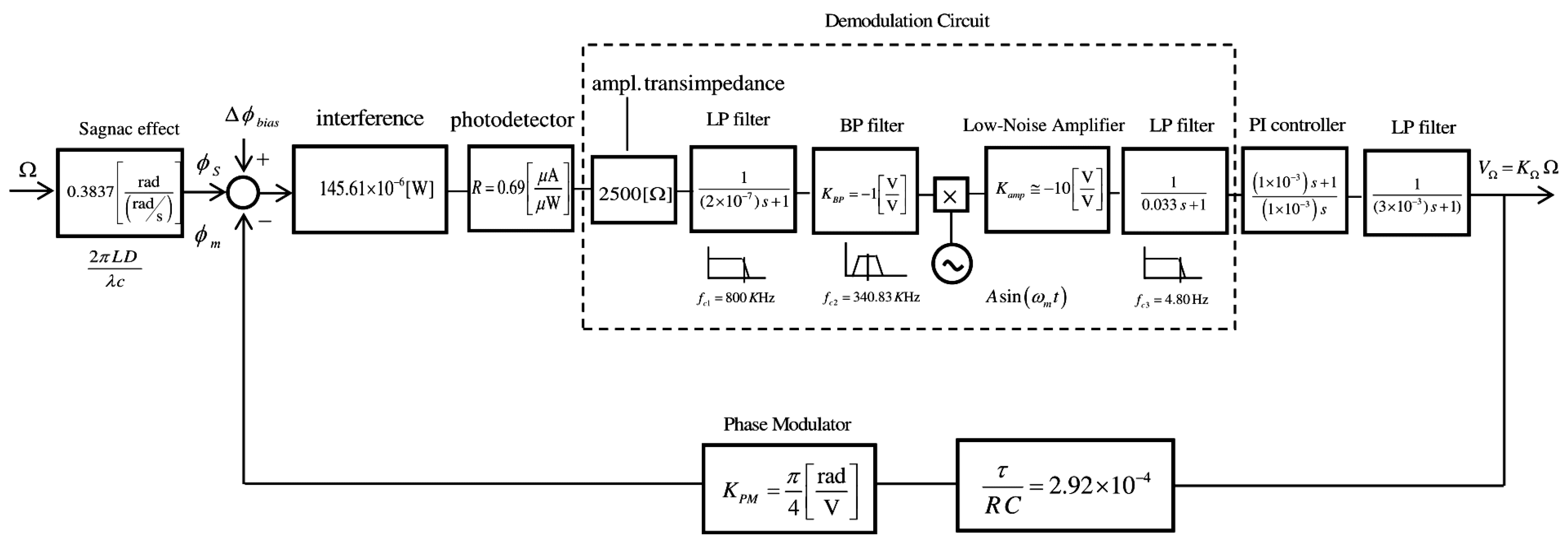
2.2. Design of the Electronic System
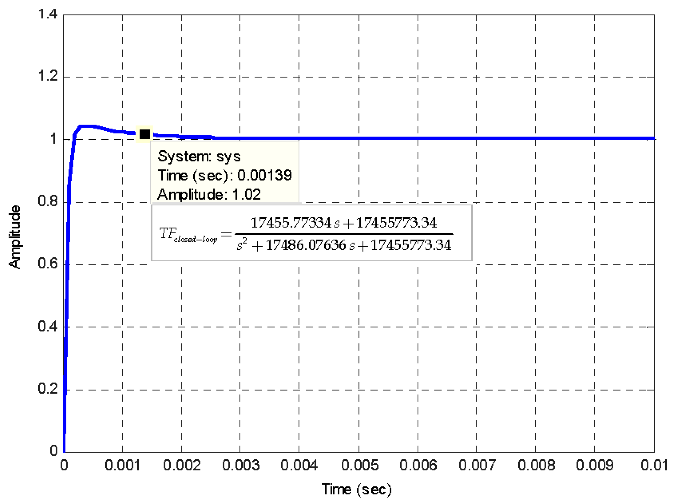
3. Calculations and Estimations
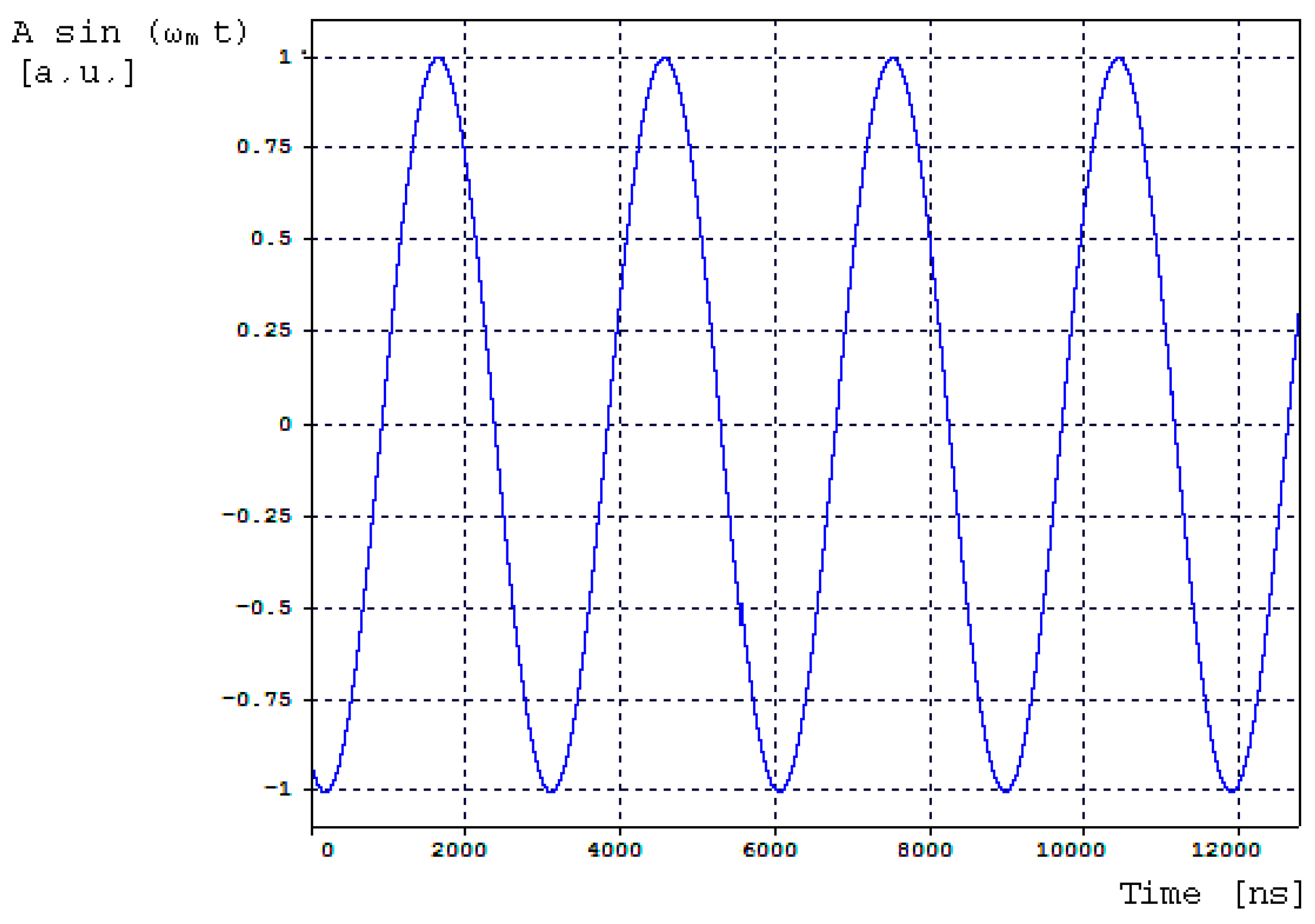
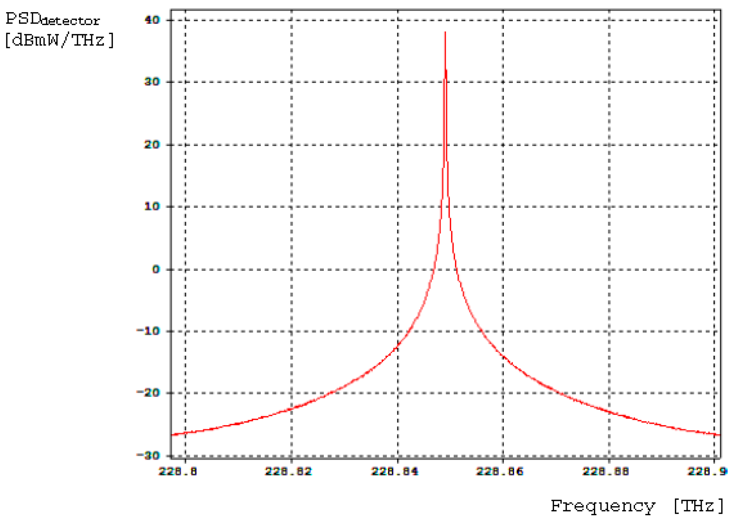
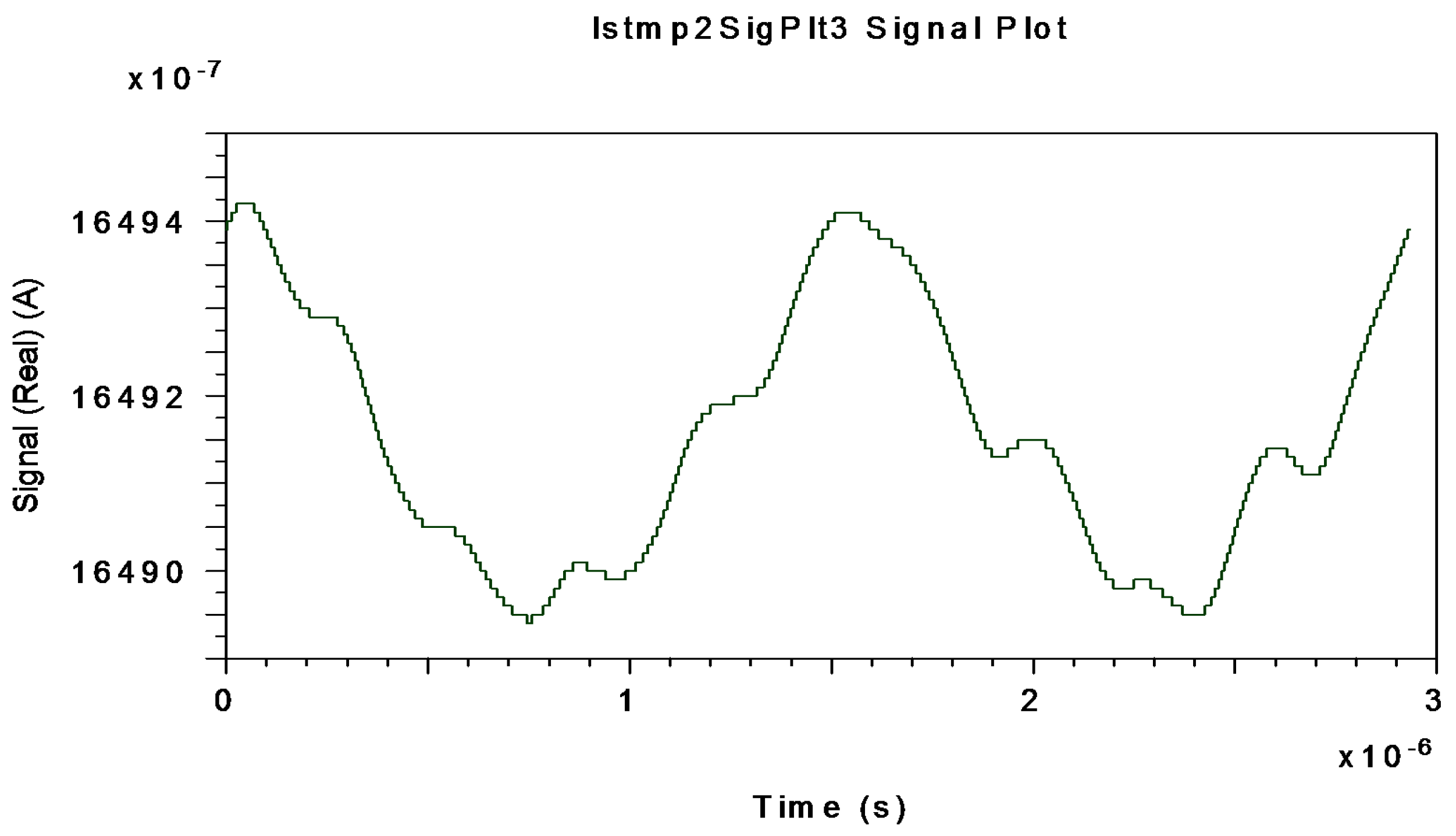
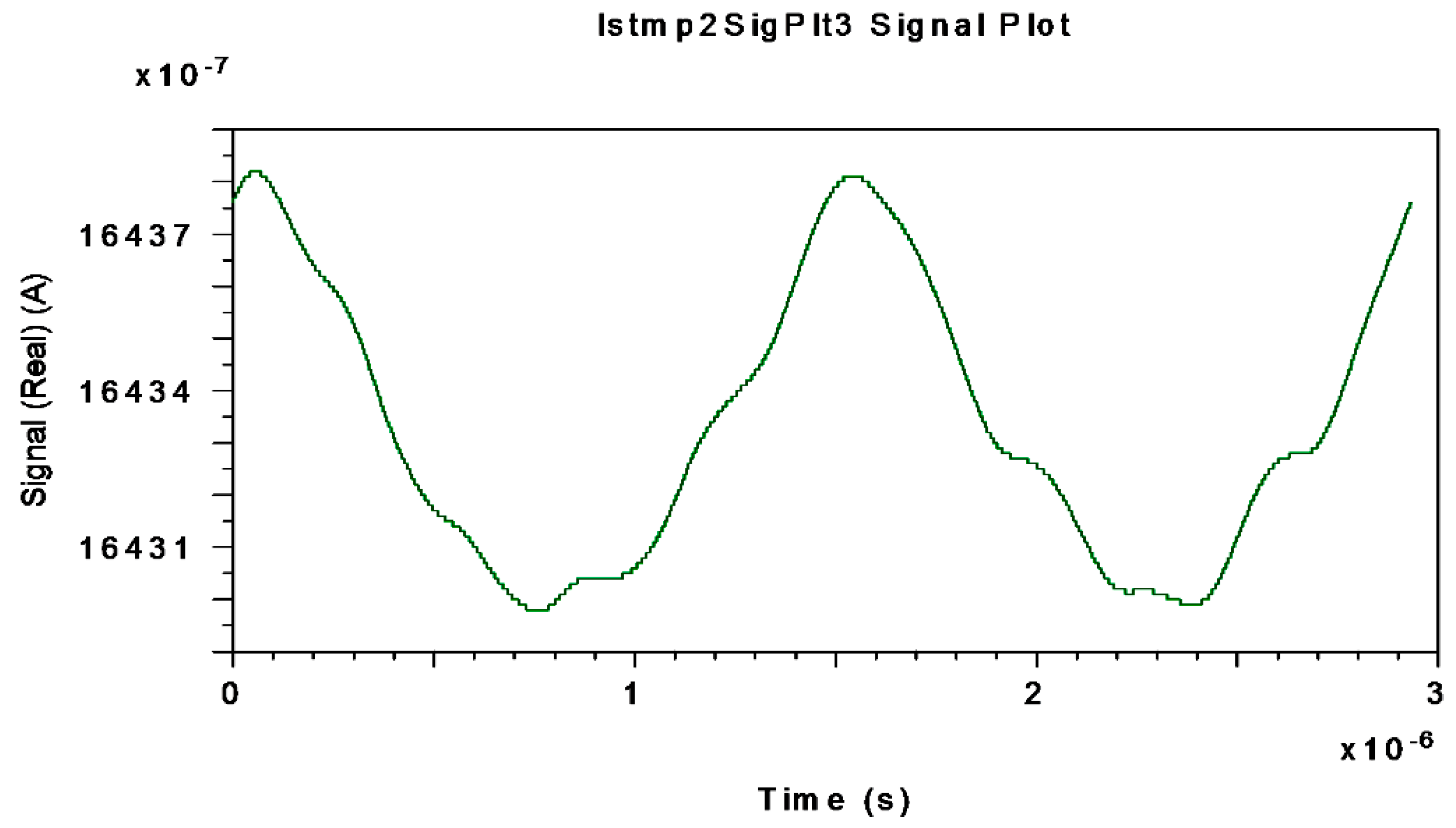
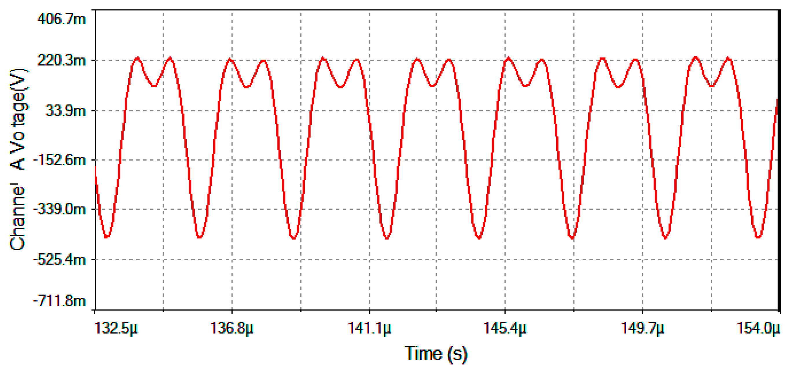
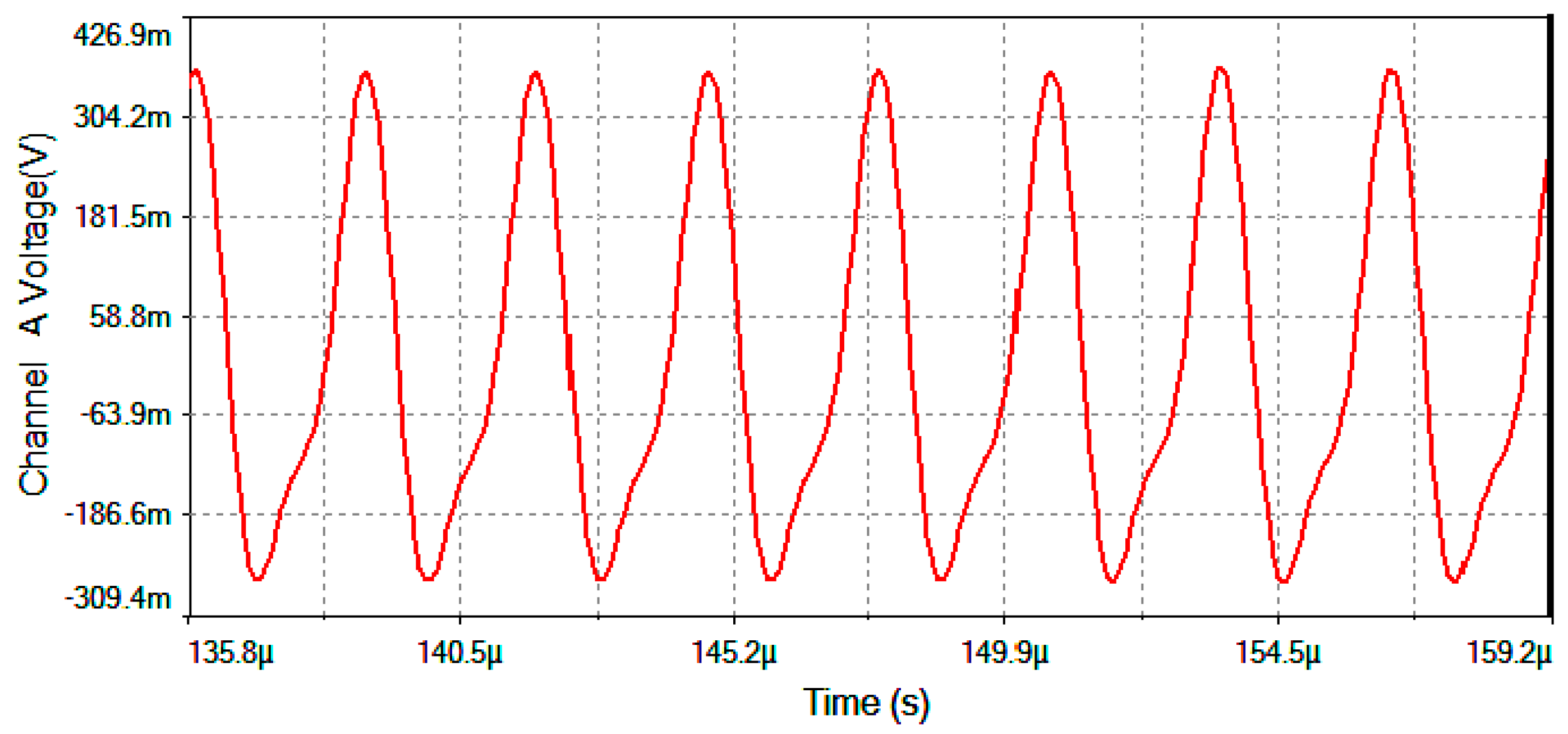
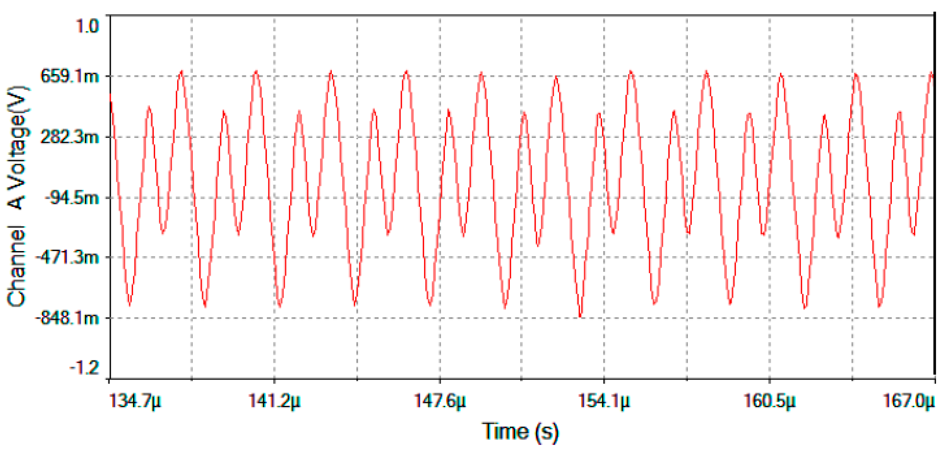
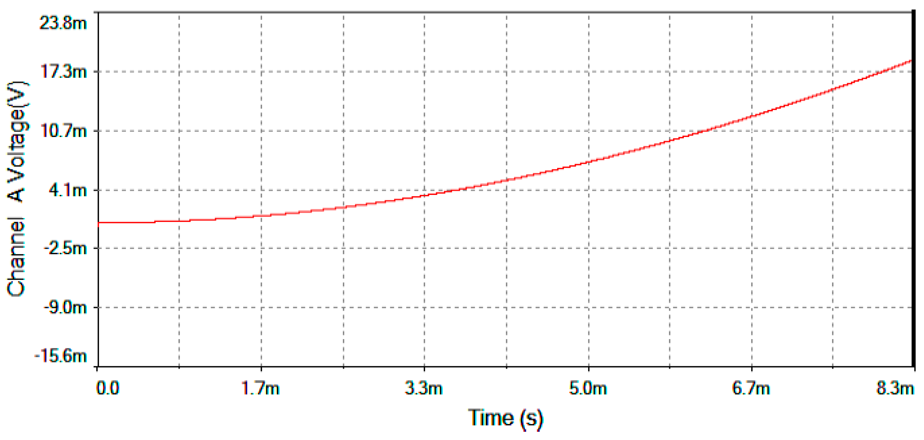
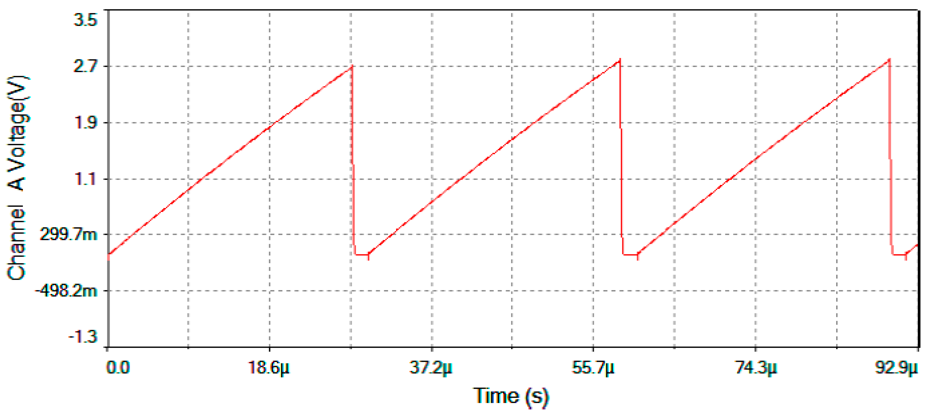
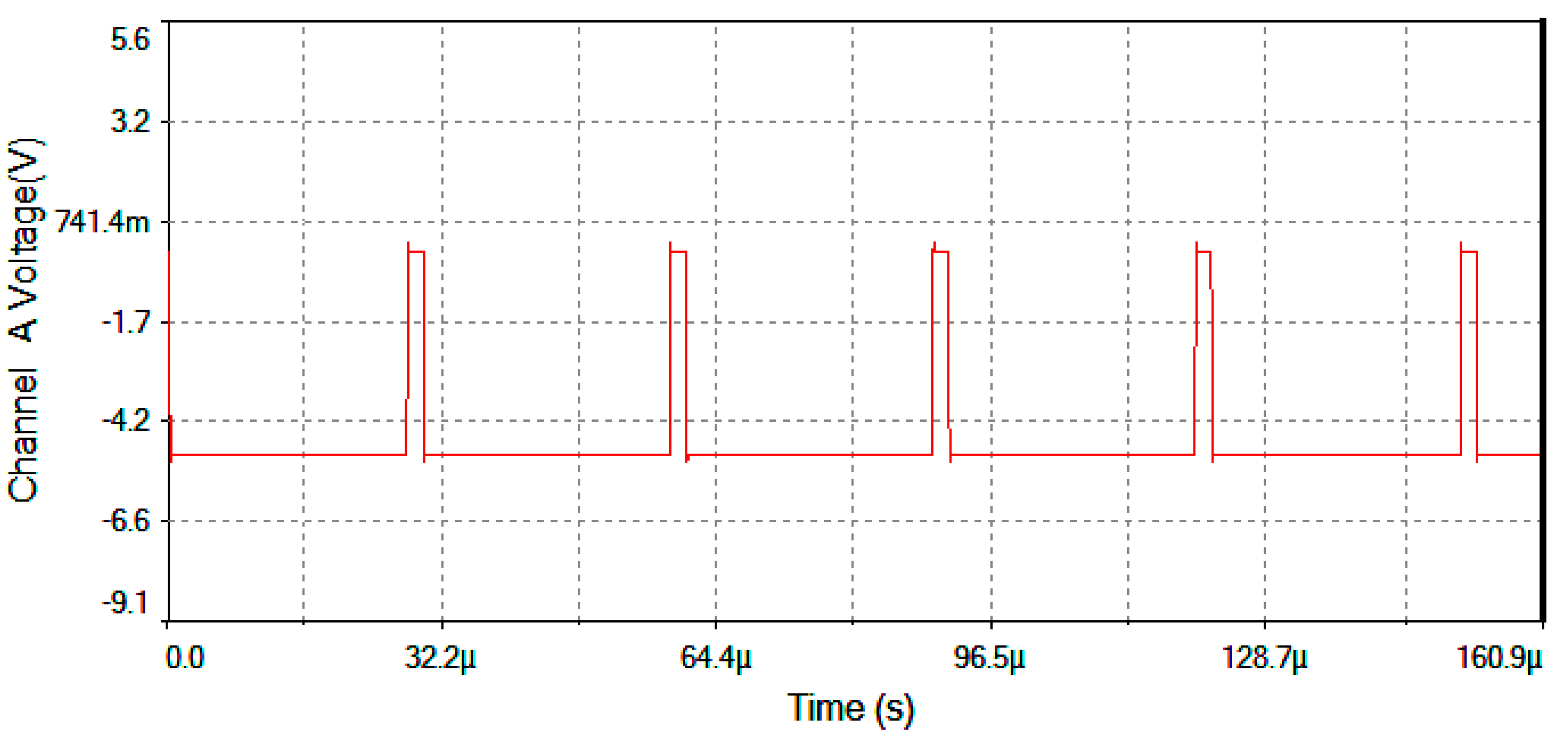
4. Simulation Results
5. Discussion of Simulation Results
6. Conclusions
Supplementary Materials
Acknowledgments
Author Contributions
Conflicts of Interest
Appendix A. Calculations
References
- Ashley, P.R.; Temmen, M.G.; Sanghadasa, M. Applications of SLDs in fiber optical gyroscopes. In Proceedings of the Test and Measurement Applications of Optoelectronic Devices 104, San Jose, CA, USA, 18 April 2002; pp. 104–115.
- Burns, W.K.; Kersey, A.D. Fiber-optic Gyroscopes with Depolarized Light. J. Light. Technol. 1992, 10, 992–998. [Google Scholar] [CrossRef]
- Szafraniec, B.; Sanders, G.A. Theory of polarization evolution in interferometric fiber-optic depolarized gyros. J. Light. Technol. 1999, 17, 579–590. [Google Scholar] [CrossRef]
- Kintner, E.C. Polarization control in optical-fiber gyroscopes. Opt. Lett. 1981, 6, 154–156. [Google Scholar] [CrossRef] [PubMed]
- Lefèvre, H.C.; Vatoux, S.; Papuchon, M.; Puech, C. Integrated optics: A practical solution for the fiber-optic gyroscope. In Proceedings of the Fiber Optic Gyros: 10th Anniversary Conference 101, Cambridge, MA, USA, 11 March 1987; pp. 101–112.
- Kim, B.Y.; Lefèvre, H.C.; Bergh, R.A.; Shaw, H.J. Response Of Fiber Gyros To Signals Introduced At The Second Harmonic Of The Bias Modulation Frequency. In Proceedings of the Single Mode Optical Fibers 86, San Diego, CA, USA, 8 November 1983. [CrossRef]
- Kim, B.Y.; Shaw, H.J. Gated phase-modulation feedback approach to fiber-optic gyroscopes. Opt. Lett. 1984, 9, 263–265. [Google Scholar] [CrossRef] [PubMed]
- Kim, B.Y.; Shaw, H.J. Gated phase-modulation approach to fiber-optic gyroscope with linearized scale factor. Opt. Lett. 1984, 9, 375–377. [Google Scholar] [CrossRef] [PubMed]
- Kim, B.Y.; Shaw, H.J. Phase reading, all-fiber-optic gyroscope. Opt. Lett. 1984, 9, 378–380. [Google Scholar] [CrossRef] [PubMed]
- Böhm, K.; Petermann, K. Signal Processing Schemes for The Fiber-Optic Gyroscope. In Proceedings of the Fiber Optic Gyros: 10th Anniversary Conference 101, Cambridge, MA, USA, 11 March 1987. [CrossRef]
- Moeller, R.P.; Burns, W.K.; Frigo, N.J. Open-loop output and scale-factor stability in a fiber-optic-gyroscope. J. Light. Technol. 1989, 7, 262–269. [Google Scholar] [CrossRef]
- Ebberg, A.; Schiffner, G. Closed-loop fiber-optic gyroscope with a sawtooth phase-modulated feedback. Opt. Lett. 1985, 10, 300–302. [Google Scholar] [CrossRef] [PubMed]
- Kay, C.J. Serrodyne modulator in a fibre-optic gyroscope. IEEE Proc. J. Optoelectron. 1985, 132, 259–264. [Google Scholar] [CrossRef]
- Yahalom, R.; Moslehi, B.; Oblea, L.; Sotoudeh, V.; Ha, J.C. Low-cost, compact fiber-optic gyroscope for super-stable line-of-sight stabilization. In Proceedings of the IEEE/ION Position Location and Navigation Symposium (PLANS), Indian Wells, CA, USA, 4–6 May 2010; pp. 180–186.
- Çelikel, O.; San, S.E. Establishment of all digital closed-loop interferometric fiber-optic-gyroscope and Scale factor comparison for open-loop and all digital closed-loop configurations. IEEE J. Sens. 2009, 9, 176–186. [Google Scholar] [CrossRef]
- Sandoval-Romero, G.E.; Nikolaev, V.A. Límite de detección de un giroscopio de fibra óptica usando una fuente de radiación superluminiscente. Rev. Mex. Fís. 2002, 49, 155–165. [Google Scholar]
- Medjadba, H.; Simohamed, L.M. Low-cost technique for improving open-loop fiber optic gyroscope scale factor linearity. In Proceedings of the International Conference on Information and Communication Technologies, Damascus, Syria, 24–28 April 2006; pp. 2057–2060.
- Bennett, S.; Emge, S.R.; Dyott, R.B. Fiber Optic Gyros for Robotics. Available online: http://www-personal.acfr.usyd.edu.au/nebot/sensors/Fiber%20Optic%20Gyro/fog_robots.pdf (accessed on 15 October 2014).
- Emge, S.; Bennet, S.M.; Dyot, R.B.; Brunner, J.; Allen, D.E. Reduced minimum configuration fiber optic gyro for land navigation applications. In Proceedings of the Fiber Optic Gyros: 20th Anniversary Conference, Denver, CO, USA, 4 August 1996. [CrossRef]
- Bennett, S.M.; Emge, S.; Dyott, R.B. Fiber optic gyroscopes for vehicular use. In Proceedings of the IEEE Conference on Intelligent Transportation System (ITSC’97), Boston, MA, USA, 9–12 November 1997; pp. 1053–1057.


| Coherence Length Lc LC >> 20 λ | Beat Length Lb | Depolarization Length LD | Lyot Depolarizer Length L1 L1 = LD | Lyot Depolarizer Length L2 L2 = 2 L1 |
|---|---|---|---|---|
| 26.20 [μm] | 13.10 [mm] | 26.20 [cm] | 26.20 [cm] | 52.40 [cm] |
| Parameter | Calculation Formula | Calculated Value | Estimated Value | Unit |
|---|---|---|---|---|
| Sensitivity Threshold | 0.05,193,796 | 0.05,193,820 | [°/h] | |
| Dynamic Range | 101.38 | 101.38 | [dB] | |
| ±78.185 | ±78.185 | [°/s] | ||
| ±1.164 × 10⁻⁵ | ±1.164 × 10⁻⁵ | [°/s] | ||
| Scale Factor | 0.3837 | 0.3664 |
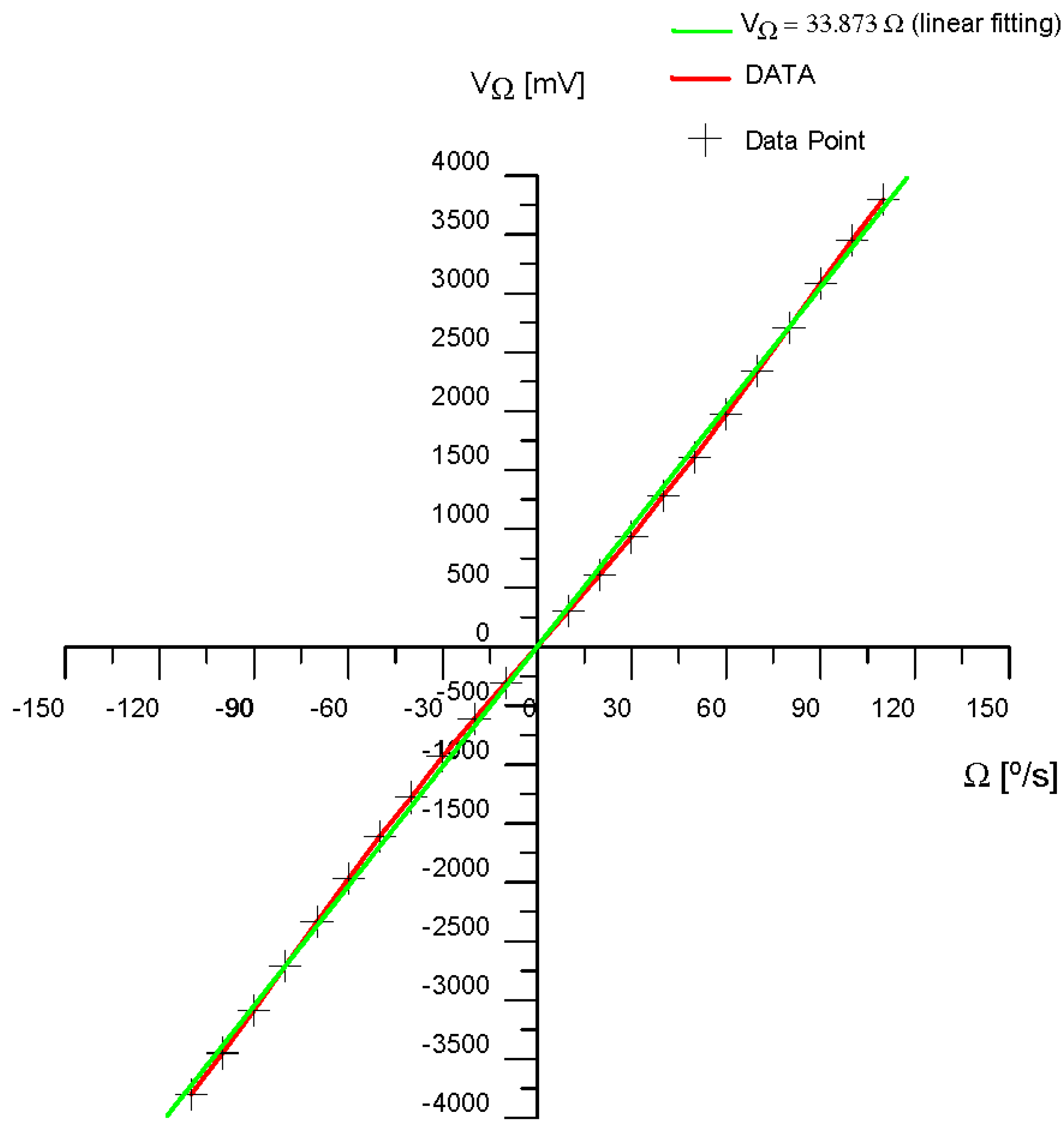
| Ω [°/s] | 0 | ±10 | ±20 | ±30 | ±40 | ±50 | ±60 | ±70 | ±80 | ±90 | ±100 | ±110 |
|---|---|---|---|---|---|---|---|---|---|---|---|---|
| VΩ [mV] | 0 | ±305 | ±613 | ±931 | ±1280 | ±1609 | ±1970 | ±2337 | ±2708 | ±3085 | ±3450 | ±3800 |
| (VΩ)lin [mV] | 0 | ±338.7 | ±677.5 | ±1016 | ±1355 | ±1694 | ±2032 | ±2371 | ±2710 | ±3049 | ±3387 | ±3726 |
| |Δ(VΩ)| [mV] | 0 | 33.73 | 64.46 | 85.19 | 74.92 | 84.65 | 62.38 | 34.11 | 1.834 | 36.44 | 62.71 | 73.98 |
| |Δ(VΩ)/ (VΩ)lin|% | 0 | 9.959 | 9.514 | 8.385 | 5.529 | 4.997 | 3.070 | 1.439 | 0.068 | 1.195 | 1.851 | 1.986 |
| Noise Source | Before Correction (ϕm = 1.80) | After Correction (ϕm = 0.9 π) |
|---|---|---|
| Photon-Shot-Noise | ΔΩ = Ωlim ≅ 0.052 [°/h] | ΔΩ = Ωlim ≅ 0.043 [°/h] |
| Excess RIN | ΔΩ = Ωlim ≅ 0.235 [°/h] | ΔΩ = Ωlim ≅ 0.015 [°/h] |
| Full Noise = Photon-Shot-Noise+ Excess RIN | ΔΩ = Ωlim ≅ 0.239 [°/h] | ΔΩ = Ωlim ≅ 0.050 [°/h] |
© 2016 by the authors; licensee MDPI, Basel, Switzerland. This article is an open access article distributed under the terms and conditions of the Creative Commons Attribution (CC-BY) license (http://creativecommons.org/licenses/by/4.0/).
Share and Cite
Pérez, R.J.; Álvarez, I.; Enguita, J.M. Theoretical Design of a Depolarized Interferometric Fiber-Optic Gyroscope (IFOG) on SMF-28 Single-Mode Standard Optical Fiber Based on Closed-Loop Sinusoidal Phase Modulation with Serrodyne Feedback Phase Modulation Using Simulation Tools for Tactical and Industrial Grade Applications. Sensors 2016, 16, 604. https://0-doi-org.brum.beds.ac.uk/10.3390/s16050604
Pérez RJ, Álvarez I, Enguita JM. Theoretical Design of a Depolarized Interferometric Fiber-Optic Gyroscope (IFOG) on SMF-28 Single-Mode Standard Optical Fiber Based on Closed-Loop Sinusoidal Phase Modulation with Serrodyne Feedback Phase Modulation Using Simulation Tools for Tactical and Industrial Grade Applications. Sensors. 2016; 16(5):604. https://0-doi-org.brum.beds.ac.uk/10.3390/s16050604
Chicago/Turabian StylePérez, Ramón José, Ignacio Álvarez, and José María Enguita. 2016. "Theoretical Design of a Depolarized Interferometric Fiber-Optic Gyroscope (IFOG) on SMF-28 Single-Mode Standard Optical Fiber Based on Closed-Loop Sinusoidal Phase Modulation with Serrodyne Feedback Phase Modulation Using Simulation Tools for Tactical and Industrial Grade Applications" Sensors 16, no. 5: 604. https://0-doi-org.brum.beds.ac.uk/10.3390/s16050604