
Effect of the Substrate Crystallinity on Morphological and Magnetic Properties of Fe70Pd30 Nanoparticles Obtained by the Solid-State Dewetting

 , , , and
Abstract
:
1. Introduction
2. Materials and Methods
3. Results
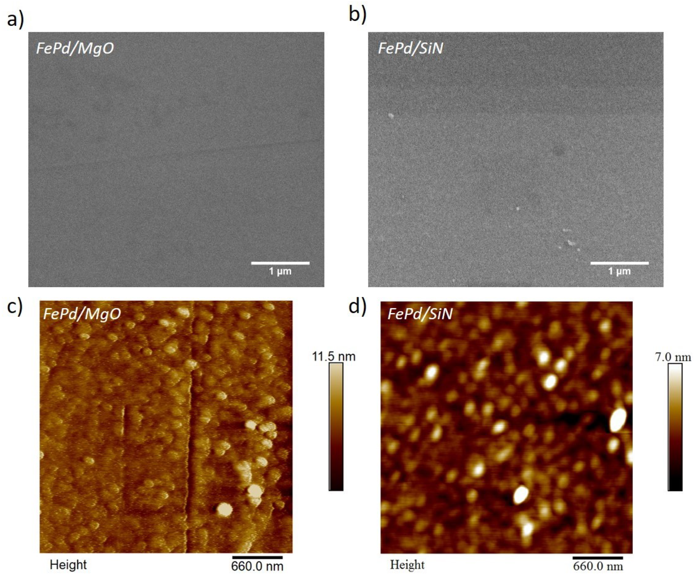
3.1. As-Deposited FePd Thin Film
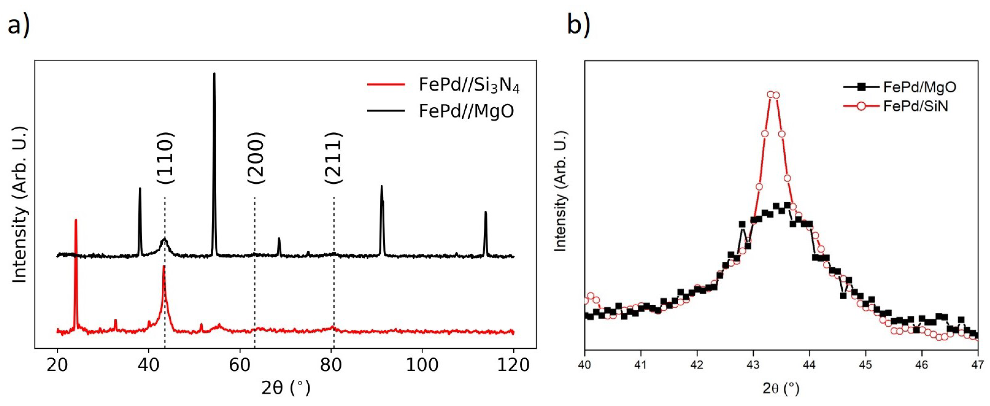
3.1.1. Structural and Morphological Characterization
3.1.2. Magnetic Properties
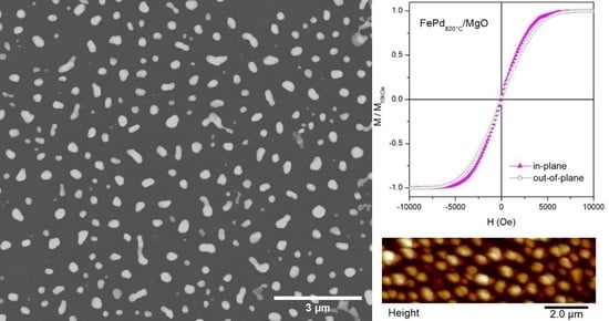
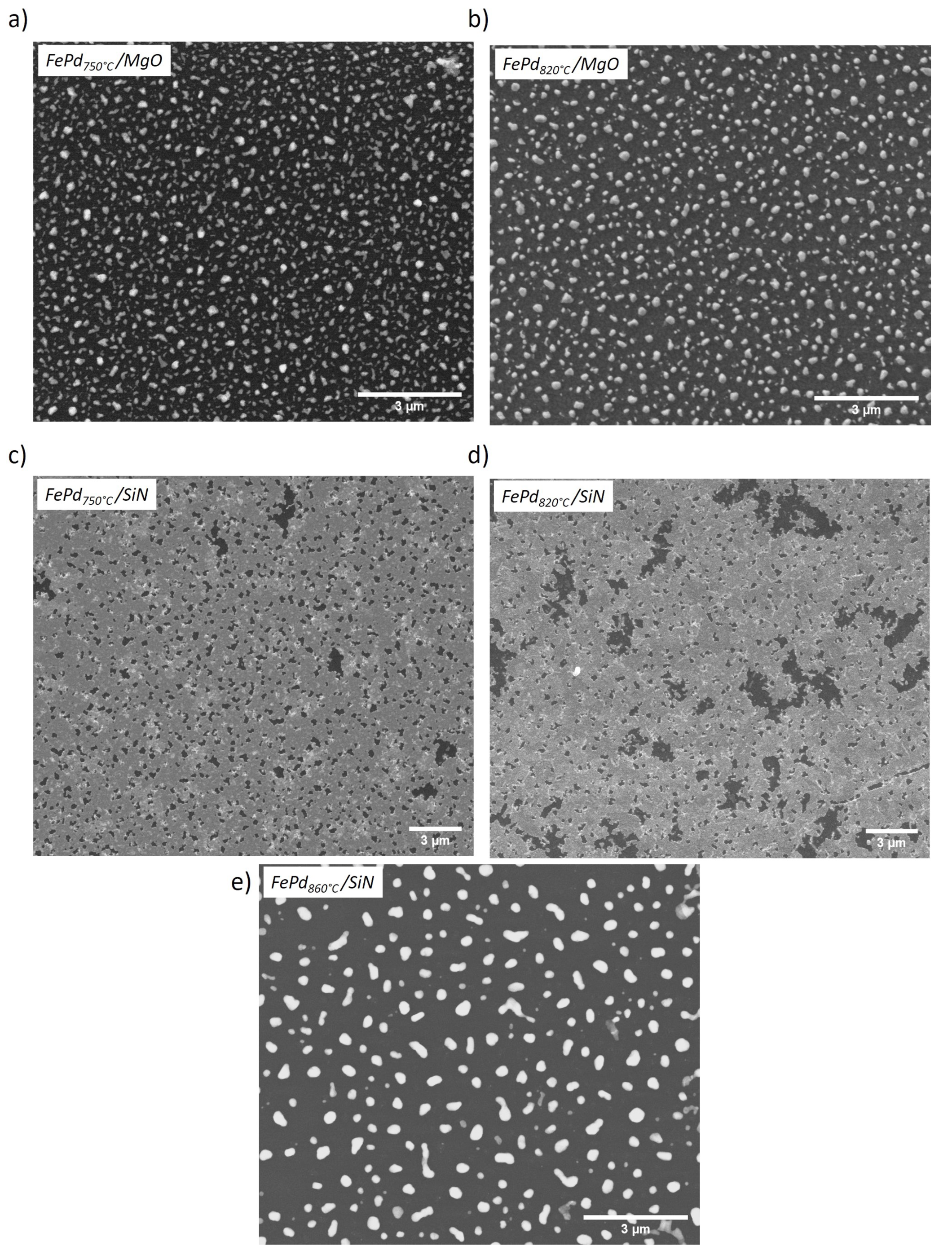
3.2. Dewetted FePd Thin Film
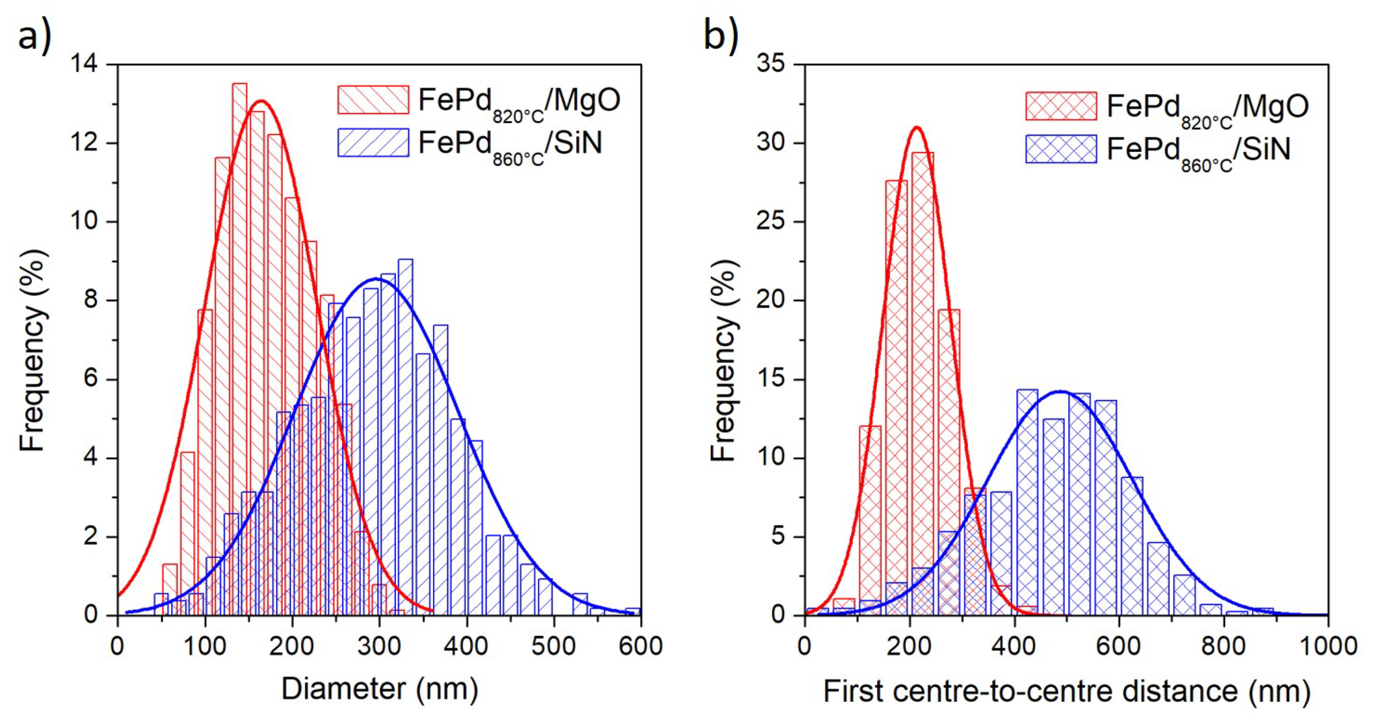
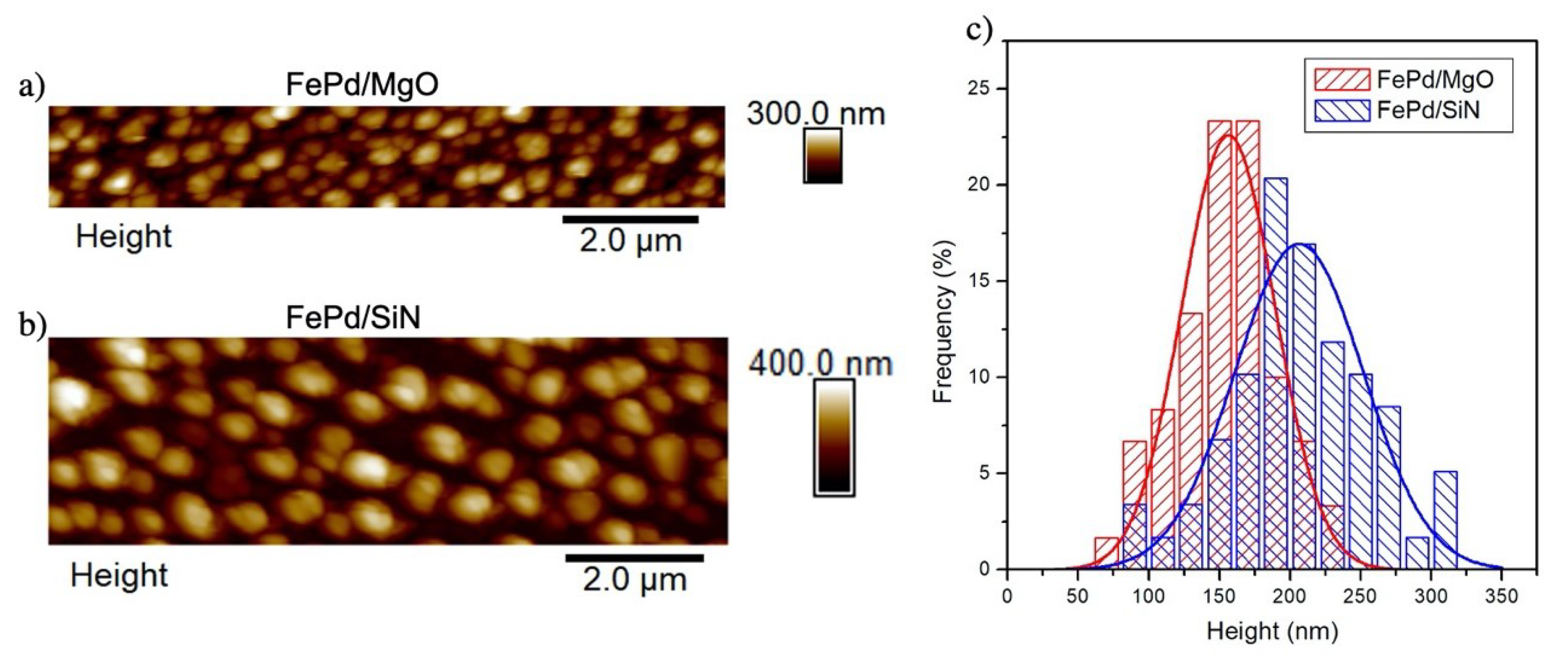
3.2.1. Structural and Morphological Characterization
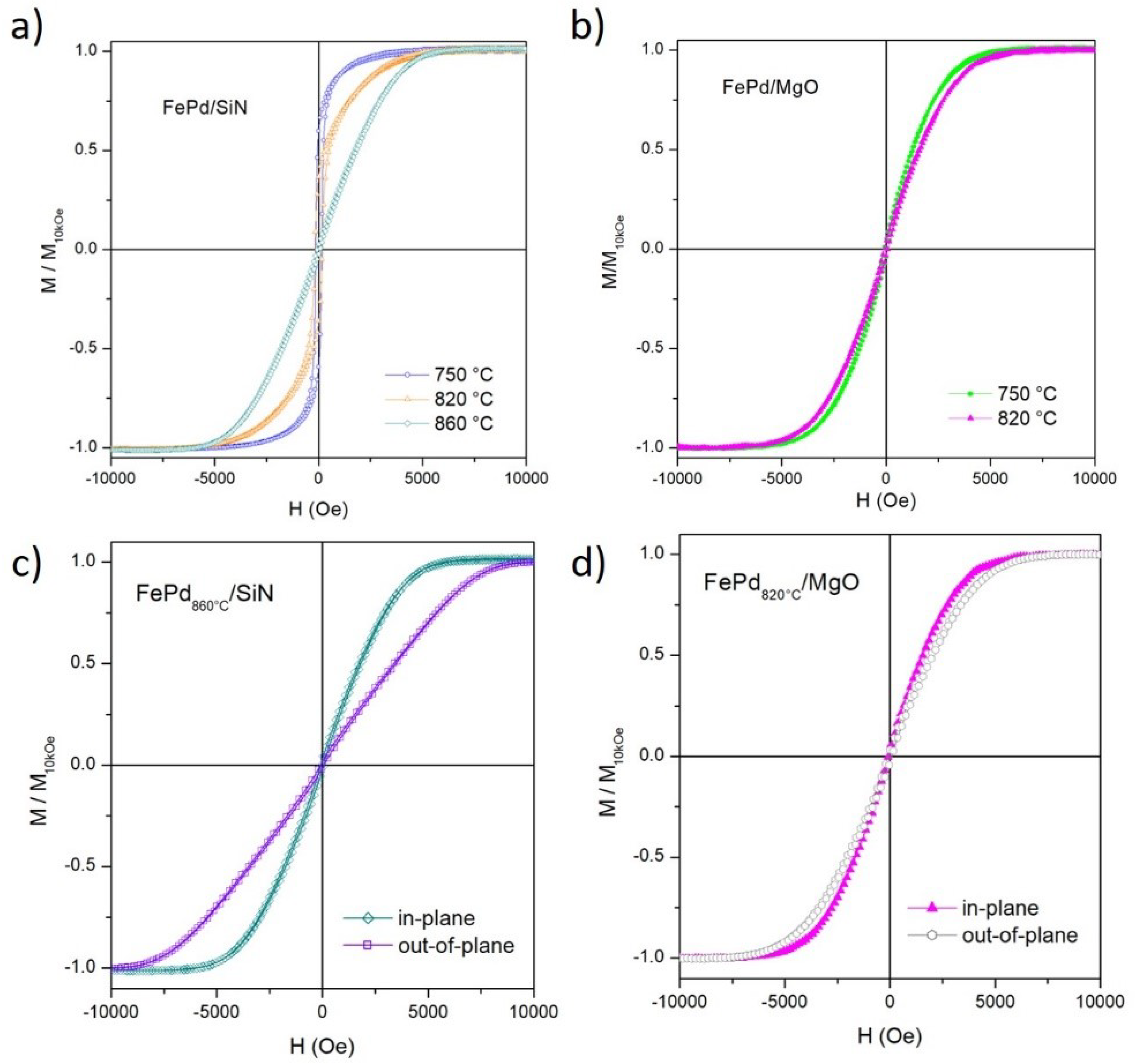
3.2.2. Magnetic Properties
4. Conclusions
Author Contributions
Funding
Institutional Review Board Statement
Informed Consent Statement
Data Availability Statement
Conflicts of Interest
References
- Arregui, F.J. Sensors Based on Nanostructured Materials; Springer Nature: Cham, Switzerland, 2009; p. 326. [Google Scholar]
- Gloag, L.; Mehdipour, M.; Chen, D.; Tilley, R.D.; Gooding, J.J. Advances in the Application of Magnetic Nanoparticles for Sensing. Adv. Mater. 2019, 31, 1904385. [Google Scholar] [CrossRef]
- Abdel-Karim, R.; Reda, Y.; Abdel-Fattah, A. Review—Nanostructured Materials-Based Nanosensors. J. Electrochem. Soc. 2020, 167, 037554. [Google Scholar] [CrossRef]
- Huang, X.J.; Choi, Y.K. Chemical sensors based on nanostructured materials. Sens. Actuators Chem. 2007, 122, 659–671. [Google Scholar] [CrossRef]
- Hahn, Y.B.; Ahmad, R.; Tripathy, N. Chemical and biological sensors based on metal oxide nanostructures. Chem. Commun. 2012, 48, 10369–10385. [Google Scholar] [CrossRef]
- Ponzoni, A.; Comini, E.; Concina, I.; Ferroni, M.; Falasconi, M.; Gobbi, E.; Sberveglieri, V.; Sberveglieri, G. Nanostructured metal oxide gas sensors, a survey of applications carried out at SENSOR lab, brescia (Italy) in the security and food quality fields. Sensors 2012, 12, 17023–17045. [Google Scholar] [CrossRef]
- Elosua, C.; Arregui, F.J.; Del Villar, I.; Ruiz-Zamarreño, C.; Corres, J.M.; Bariain, C.; Goicoechea, J.; Hernaez, M.; Rivero, P.J.; Socorro, A.B.; et al. Micro and nanostructured materials for the development of optical fibre sensors. Sensors 2017, 17, 2312. [Google Scholar] [CrossRef] [Green Version]
- Nasiri, N.; Clarke, C. Nanostructured gas sensors for medical and health applications: Low to high dimensional materials. Biosensors 2019, 9, 43. [Google Scholar] [CrossRef] [PubMed] [Green Version]
- Antonacci, A.; Arduini, F.; Moscone, D.; Palleschi, G.; Scognamiglio, V. Nanostructured (Bio)sensors for smart agriculture. Trac—Trends Anal. Chem. 2018, 98, 95–103. [Google Scholar] [CrossRef]
- Huynh, T.P. Chemical and biological sensing with nanocomposites prepared from nanostructured copper sulfides. Nano Futures 2020, 4, 032001. [Google Scholar] [CrossRef]
- Barua, S.; Dutta, H.S.; Gogoi, S.; Devi, R.; Khan, R. Nanostructured MoS2-Based Advanced Biosensors: A Review. ACS Appl. Nano Mater. 2018, 1, 2–25. [Google Scholar] [CrossRef]
- Di Pietrantonio, F.; Cannatà, D.; Benetti, M. Biosensor technologies based on nanomaterials. Funct. Nanostruct. Interfaces Environ. Biomed. Appl. 2019, 181–242. [Google Scholar] [CrossRef]
- Lee, H.B.; Meeseepong, M.; Trung, T.Q.; Kim, B.Y.; Lee, N.E. A wearable lab-on-a-patch platform with stretchable nanostructured biosensor for non-invasive immunodetection of biomarker in sweat. Biosens. Bioelectron. 2020, 156, 112133. [Google Scholar] [CrossRef] [PubMed]
- Santos, A.; Deen, M.J.; Marsal, L.F. Low-cost fabrication technologies for nanostructures: State-of-the-art and potential. Nanotechnology 2015, 26, 042001. [Google Scholar] [CrossRef]
- Stepanova, M. Nanofabrication: Techniques and Principles; Springer: Berlin/Heidelberg, Germany, 2012. [Google Scholar]
- Prasad, S.; Kumar, V.; Kirubanandam, S.; Barhoum, A. Engineered nanomaterials: Nanofabrication and surface functionalization. In Emerging Applications of Nanoparticles and Architectural Nanostructures: Current Prospects and Future Trends; Elsevier: Amsterdam, The Netherlands, 2018; pp. 305–340. [Google Scholar] [CrossRef]
- Kim, D.; Giermann, A.L.; Thompson, C.V. Solid-state dewetting of patterned thin films. Appl. Phys. Lett. 2009, 95, 2–4. [Google Scholar] [CrossRef]
- Thompson, C.V. Solid-State Dewetting of Thin Films. Annu. Rev. Mater. Res. 2012, 42, 399–434. [Google Scholar] [CrossRef]
- Andalouci, A.; Roussigné, Y.; Farhat, S.; Chérif, S.M. Magnetic and magneto-optical properties of assembly of nanodots obtained from solid-state dewetting of ultrathin cobalt layer. J. Phys. Condens. Matter 2019, 31, 495805. [Google Scholar] [CrossRef] [PubMed]
- Garfinkel, D.A.; Pakeltis, G.; Tang, N.; Ivanov, I.N.; Fowlkes, J.D.; Gilbert, D.A.; Rack, P.D. Optical and Magnetic Properties of Ag-Ni Bimetallic Nanoparticles Assembled via Pulsed Laser-Induced Dewetting. ACS Omega 2020, 5, 19285–19292. [Google Scholar] [CrossRef] [PubMed]
- Pengphorm, P.; Nuchuay, P.; Boonrod, N.; Boonsit, S.; Srisamran, P.; Thongrom, S.; Pewkum, P.; Kalasuwan, P.; van Dommelen, P.; Daengngam, C. Fabrication of 3D surface-enhanced Raman scattering (SERS) substrate via solid-state dewetting of sputtered gold on fumed silica surface. J. Phys. Conf. Ser. 2021, 1719, 012082. [Google Scholar] [CrossRef]
- Oh, H.; Pyatenko, A.; Lee, M. A hybrid dewetting approach to generate highly sensitive plasmonic silver nanoparticles with a narrow size distribution. Appl. Surf. Sci. 2021, 542, 148613. [Google Scholar] [CrossRef]
- Nsimama, P.D.; Herz, A.; Wang, D.; Schaaf, P. Influence of the substrate on the morphological evolution of gold thin films during solid-state dewetting. Appl. Surf. Sci. 2016, 388, 475–482. [Google Scholar] [CrossRef]
- Barrera, G.; Celegato, F.; Coïsson, M.; Cialone, M.; Rizzi, P.; Tiberto, P. Formation of free-standing magnetic particles by solid-state dewetting of Fe80Pd20 thin films. J. Alloys Compd. 2018, 742. [Google Scholar] [CrossRef] [Green Version]
- Esterina, R.; Liu, X.M.; Adeyeye, A.O.; Ross, C.A.; Choi, W.K. Solid-state dewetting of magnetic binary multilayer thin films. J. Appl. Phys. 2015, 118, 144902. [Google Scholar] [CrossRef]
- Bhalla, N.; Jain, A.; Lee, Y.; Shen, A.Q.; Lee, D. Dewetting Metal Nanofilms—Effect of Substrate on Refractive Index Sensitivity of Nanoplasmonic Gold. Nanomaterials 2019, 9, 1530. [Google Scholar] [CrossRef] [PubMed] [Green Version]
- Song, X.; Liu, F.; Qiu, C.; Coy, E.; Liu, H.; Aperador, W.; Zaleski, K.; Li, J.J.; Song, W.; Lu, Z.; et al. Nanosurfacing Ti alloy by weak alkalinity-activated solid-state dewetting (AAD) and its biointerfacial enhancement effect. Mater. Horiz. 2021, 8, 912–924. [Google Scholar] [CrossRef]
- Quan, J.; Zhang, J.; Qi, X.; Li, J.; Wang, N.; Zhu, Y. A study on the correlation between the dewetting temperature of Ag film and SERS intensity. Sci. Rep. 2017, 7, 1–12. [Google Scholar] [CrossRef] [Green Version]
- Andrikaki, S.; Govatsi, K.; Yannopoulos, S.N.; Voyiatzis, G.A.; Andrikopoulos, K.S. Thermal dewetting tunes surface enhanced resonance Raman scattering (SERRS) performance. RSC Adv. 2018, 8, 29062–29070. [Google Scholar] [CrossRef] [Green Version]
- Wang, L.W.; Cheng, C.F.; Liao, J.W.; Wang, C.Y.; Wang, D.S.; Huang, K.F.; Lin, T.Y.; Ho, R.M.; Chen, L.J.; Lai, C.H. Thermal dewetting with a chemically heterogeneous nano-template for self-assembled L10 FePt nanoparticle arrays. Nanoscale 2016, 8, 3926–3935. [Google Scholar] [CrossRef] [PubMed] [Green Version]
- Preger, C.; Bulbucan, C.; Meuller, B.O.; Ludvigsson, L.; Kostanyan, A.; Muntwiler, M.; Deppert, K.; Westerström, R.; Messing, M.E. Controlled Oxidation and Self-Passivation of Bimetallic Magnetic FeCr and FeMn Aerosol Nanoparticles. J. Phys. Chem. C 2019, 123, 16083–16090. [Google Scholar] [CrossRef] [Green Version]
- Sharma, G.; Kumar, A.; Sharma, S.; Naushad, M.; Prakash Dwivedi, R.; ALOthman, Z.A.; Mola, G.T. Novel development of nanoparticles to bimetallic nanoparticles and their composites: A review. J. King Saud Univ. Sci. 2019, 31, 257–269. [Google Scholar] [CrossRef]
- Ragothaman, M.; Mekonnen, B.T.; Palanisamy, T. Synthesis of magnetic Fe–Cr bimetallic nanoparticles from industrial effluents for smart material applications. Mater. Chem. Phys. 2020, 253, 123405. [Google Scholar] [CrossRef]
- Elanchezhiyan, S.S.; Muthu Prabhu, S.; Kim, Y.; Park, C.M. Lanthanum-substituted bimetallic magnetic materials assembled carboxylate-rich graphene oxide nanohybrids as highly efficient adsorbent for perfluorooctanoic acid adsorption from aqueous solutions. Appl. Surf. Sci. 2020, 509, 144716. [Google Scholar] [CrossRef]
- Tiberto, P.; Celegato, F.; Barrera, G.; Coisson, M.; Vinai, F.; Rizzi, P. Magnetization reversal and microstructure in polycrystalline Fe50Pd50 dot arrays by self-assembling of polystyrene nanospheres. Sci. Technol. Adv. Mater. 2016, 17, 462–472. [Google Scholar] [CrossRef] [PubMed] [Green Version]
- Shao, Z.; An, L.; Li, Z.; Huang, Y.; Hu, Y.; Ren, S. Eutectic crystallized FePd nanoparticles for liquid metal magnet. Chem. Commun. 2020, 56, 6555–6558. [Google Scholar] [CrossRef] [PubMed]
- Yang, C.; Feng, W.; Li, Y.; Tian, X.; Zhou, Z.; Lu, L.; Nie, Y. A promising method for diabetes early diagnosis via sensitive detection of urine glucose by Fe–Pd/rGO. Dye. Pigment. 2019, 164, 20–26. [Google Scholar] [CrossRef]
- Yang, Y.; Lyu, M.; Li, J.H.; Zhu, D.M.; Yuan, Y.F.; Liu, W. Ultra-small bimetallic iron-palladium (FePd) nanoparticle loaded macrophages for targeted tumor photothermal therapy in NIR-II biowindows and magnetic resonance imaging. RSC Adv. 2019, 9, 33378–33387. [Google Scholar] [CrossRef] [Green Version]
- Yamamoto, S.; Takao, S.; Muraishi, S.; Xu, C.; Taya, M. Synthesis of Fe70Pd30 nanoparticles and their surface modification by zwitterionic linker. Mater. Chem. Phys. 2019, 234, 237–244. [Google Scholar] [CrossRef]
- Kwon, J.; Mao, X.; Lee, H.A.; Oh, S.; Tufa, L.T.; Choi, J.Y.; Kim, J.E.; Kim, C.Y.; Kim, J.G.; Hwang, D.Y.; et al. Iron–Palladium magnetic nanoparticles for decolorizing rhodamine B and scavenging reactive oxygen species. J. Colloid Interface Sci. 2021, 588, 646–656. [Google Scholar] [CrossRef]
- Zheng, G.; Mourdikoudis, S.; Zhang, Z. Plasmonic Metallic Heteromeric Nanostructures. Small 2020, 16, 2002588. [Google Scholar] [CrossRef]
- Cialone, M.; Celegato, F.; Scaglione, F.; Barrera, G.; Raj, D.; Coïsson, M.; Tiberto, P.; Rizzi, P. Nanoporous FePd alloy as multifunctional ferromagnetic SERS-active substrate. Appl. Surf. Sci. 2021, 543, 148759. [Google Scholar] [CrossRef]
- Smilgies, D.M. Scherrer grain-size analysis adapted to grazing-incidence scattering with area detectors. J. Appl. Crystallogr. 2009, 42, 1030–1034. [Google Scholar] [CrossRef] [Green Version]
- Schneider, C.; Rasband, W.; Eliceiri, K. NIH Image to ImageJ: 25 Years of image analysis. Nat. Methods 2012, 9, 671–675. [Google Scholar] [CrossRef]
- Thornton, J.A. Influence of substrate temperature and deposition rate on structure of thick sputtered Cu coatings. J. Vac. Sci. Technol. 1975, 12, 830–835. [Google Scholar] [CrossRef]
- Ibru, T.; Kalaitzidou, K.; Kevin Baldwin, J.; Antoniou, A. Stress-induced surface instabilities and defects in thin films sputter deposited on compliant substrates. Soft Matter 2017, 13, 4035–4046. [Google Scholar] [CrossRef] [PubMed]
- Cialone, M.; Celegato, F.; Coïsson, M.; Barrera, G.; Fiore, G.; Shvab, R.; Klement, U.; Rizzi, P.; Tiberto, P. Tailoring magnetic properties of multicomponent layered structure via current annealing in FePd thin films. Sci. Rep. 2017, 7, 16691. [Google Scholar] [CrossRef] [PubMed] [Green Version]
- Cialone, M.; Fernandez-Barcia, M.; Celegato, F.; Coisson, M.; Barrera, G.; Uhlemann, M.; Gebert, A.; Sort, J.; Pellicer, E.; Rizzi, P.; et al. A comparative study of the influence of the deposition technique (electrodeposition versus sputtering) on the properties of nanostructured Fe70Pd30 films. Sci. Technol. Adv. Mater. 2020, 21, 424–434. [Google Scholar] [CrossRef] [PubMed]
- Weisheit, M.; Schultz, L.; Fähler, S. Textured growth of highly coercive L10 ordered FePt thin films on single crystalline and amorphous substrates. J. Appl. Phys. 2004, 95, 7489–7491. [Google Scholar] [CrossRef]
- Seki, K.; Kura, H.; Sato, T.; Taniyama, T. Size dependence of martensite transformation temperature in ferromagnetic shape memory alloy FePd. J. Appl. Phys. 2008, 103, 063910. [Google Scholar] [CrossRef]
- Cullity, B.D.; Graham, C.D. Introduction to Magnetic Materials; Wiley-IEEE Press: Hoboken, NJ, USA, 2009. [Google Scholar]
- Porter, A.A.; Easterling, K.E.; Sherif, M.Y. Phase Transformations in Metals and Alloys, 3rd ed.; Routledge: London, UK, 2009; p. 536. [Google Scholar]
- Srolovitz, D. Capillary instabilities in thin films. I. Energetics. J. Appl. Phys. 1986, 60, 247–254. [Google Scholar] [CrossRef]
- Gazit, N.; Klinger, L.; Rabkin, E. Chemically-induced solid-state dewetting of thin Au films. Acta Mater. 2017, 129, 300–311. [Google Scholar] [CrossRef]
- Wynblatt, P. Interfacial segregation effects in wetting phenomena. Annu. Rev. Mater. Res. 2008, 38, 173–196. [Google Scholar] [CrossRef]
- Amram, D.; Klinger, L.; Rabkin, E. Phase transformations in Au(Fe) nano-and microparticles obtained by solid state dewetting of thin Au-Fe bilayer films. Acta Mater. 2013, 61, 5130–5143. [Google Scholar] [CrossRef]
- Herre, P.; Will, J.; Dierner, M.; Wang, D.; Yokosawa, T.; Zech, T.; Wu, M.; Przybilla, T.; Romeis, S.; Unruh, T.; et al. Rapid fabrication and interface structure of highly faceted epitaxial Ni-Au solid solution nanoparticles on sapphire. Acta Mater. 2021, 220, 117318. [Google Scholar] [CrossRef]
- Barda, H.; Rabkin, E. Improving the thermal stability of nickel thin films on sapphire by a minor alloying addition of gold. Appl. Surf. Sci. 2019, 484, 1070–1079. [Google Scholar] [CrossRef]
- Li, Y.; Yang, B.; Xia, M.; Yang, F.; Bao, X. Oxidation-induced segregation of FeO on the Pd-Fe alloy surface. Appl. Surf. Sci. 2020, 525, 146484. [Google Scholar] [CrossRef]
- Vahalia, U.; Dowben, P.A.; Miller, A. Surface segregation in binary alloys. J. Vac. Sci. Technol. A 1986, 4, 1675–1679. [Google Scholar] [CrossRef]
- Sakurai, T.; Hashizume, T.; Kobyashi, A.; Sakai, A.; Hyodo, S. Surface segregation of Ni-Cu binary alloys studied by an atom-probe. Phys. Rev. B 1986, 34, 8379. [Google Scholar] [CrossRef] [PubMed]
- Zheng, J.; Zhu, Y.; Zeng, X.; Chen, B. Segregation of solute atoms in Mg–Ce binary alloy: Atomic-scale novel structures observed by HAADF-STEM. Philos. Mag. 2017, 97, 1498–1508. [Google Scholar] [CrossRef]
- Oh, Y.J.; Ross, C.A.; Jung, Y.S.; Wang, Y.; Thompson, C.V. Cobalt nanoparticle arrays made by templated solid-state dewetting. Small 2009, 5, 860–865. [Google Scholar] [CrossRef]


| FePd/SiN | FePd/MgO | |||
|---|---|---|---|---|
| 750 °C | 9.1 × 10 | 147 | 5.3 × 10 | 92 |
| 820 °C | 4.2 × 10 | 177 | 4.1 × 10 | 88 |
| 860 °C | 3.5 × 10 | 73 | - | - |
Publisher’s Note: MDPI stays neutral with regard to jurisdictional claims in published maps and institutional affiliations. |
© 2021 by the authors. Licensee MDPI, Basel, Switzerland. This article is an open access article distributed under the terms and conditions of the Creative Commons Attribution (CC BY) license (https://creativecommons.org/licenses/by/4.0/).
Share and Cite
Barrera, G.; Celegato, F.; Cialone, M.; Coïsson, M.; Rizzi, P.; Tiberto, P. Effect of the Substrate Crystallinity on Morphological and Magnetic Properties of Fe70Pd30 Nanoparticles Obtained by the Solid-State Dewetting. Sensors 2021, 21, 7420. https://0-doi-org.brum.beds.ac.uk/10.3390/s21217420
Barrera G, Celegato F, Cialone M, Coïsson M, Rizzi P, Tiberto P. Effect of the Substrate Crystallinity on Morphological and Magnetic Properties of Fe70Pd30 Nanoparticles Obtained by the Solid-State Dewetting. Sensors. 2021; 21(21):7420. https://0-doi-org.brum.beds.ac.uk/10.3390/s21217420
Chicago/Turabian StyleBarrera, Gabriele, Federica Celegato, Matteo Cialone, Marco Coïsson, Paola Rizzi, and Paola Tiberto. 2021. "Effect of the Substrate Crystallinity on Morphological and Magnetic Properties of Fe70Pd30 Nanoparticles Obtained by the Solid-State Dewetting" Sensors 21, no. 21: 7420. https://0-doi-org.brum.beds.ac.uk/10.3390/s21217420