Article

Adaptive and Nonlinear Control Techniques Applied to SEPIC Converter in DC-DC, PFC, CCM and DCM Modes Using HIL Simulation

by
Arthur H. R. Rosa
*,†,
Thiago M. De Souza
,
Lenin M. F. Morais
and
Seleme I. Seleme, Jr.
Graduate Program in Electrical Engineering, Universidade Federal de Minas Gerais, Av. Antônio Carlos 6627, 31270-901 Belo Horizonte, MG, Brazil
*
Author to whom correspondence should be addressed.
These authors contributed equally to this work.
Submission received: 31 January 2018 / Revised: 20 February 2018 / Accepted: 24 February 2018 / Published: 9 March 2018

Abstract

:
In this paper, we propose adaptive nonlinear controllers for the Single-Ended Primary Inductance Converter (SEPIC). We also consider four distinct situations: AC-DC, DC-DC, Continuous Conduction Mode (CCM) and Discontinuous Conduction Mode (DCM). A comparative analysis between classic linear and nonlinear approaches to regulate the control loop is made. Three adaptive nonlinear control laws are designed: Feedback Linearization Control (FLC), Passivity-Based Control (PBC) and Interconnection and Damping Assignment Passivity-Based Control (IDAPBC). In order to compare the performance of these control techniques, numerical simulations were made in Software and Hardware in the Loop (HIL) for nominal conditions and operation disturbances. We recommend adaptive controllers for the two different situations: Adaptive Passivity-Based Feedback Linearization Control (APBFLC) for the PFC (Power Factor Correction) AC-DC system and IDAPBC-BB (IDAPBC Based on Boost converter) for the regulator DC-DC system.

1. Introduction

Conventional power supplies usually only have one full-bridge diode rectifier and one large capacitive filter in the input stage. This front-end circuit operates with a high Total Harmonic Distortion (THDi) in the grid current, a low power factor (0.5–0.7) and normally does not meet regulatory standards, such as the important international standard IEC 61000-3-2 [
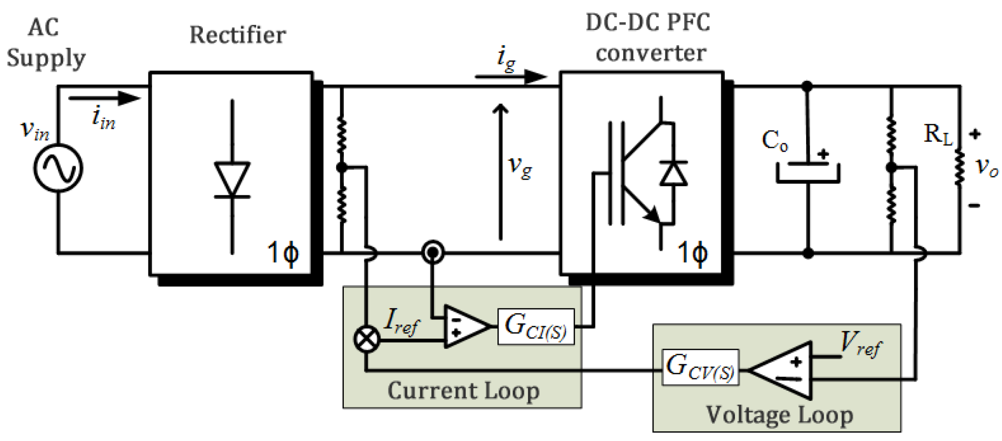
1]. Among the possible alternatives to improve the performance of switched sources, a highlight is the use of a DC-DC converter to creation a Power Factor Correction (PFC) system. As shown in Figure 1, this solution makes it possible to build nearly ideal rectifiers (emulates a resistor) and still achieve voltage, current or power regulation.
Several topologies of converters used in power factor correction are present in the literature [2,3]. Among them, the most popular topology is the boost converter [4,5]. However, this converter has some disadvantages:
  • Relatively high output voltage (at least equal to the AC source voltage), which can generate over-voltage stress in the switches;
  • Difficulty in implementing insulation between input and output;
  • Lack of overload and over-current control due to the absence of a serial switch between the input and the output;
  • Inability to start-up.
However, the CUK and SEPIC topologies overcome these drawbacks presented by the boost converter, which becomes a good choice in PFC applications. In time, SEPIC converters have attracted much attention from modern applications, especially those involving renewable energy [6] such as LED (Light Emitting Diode) [7,8], fuel cells [9], battery chargers [10], photovoltaics [11] and eolic systems [12,13].
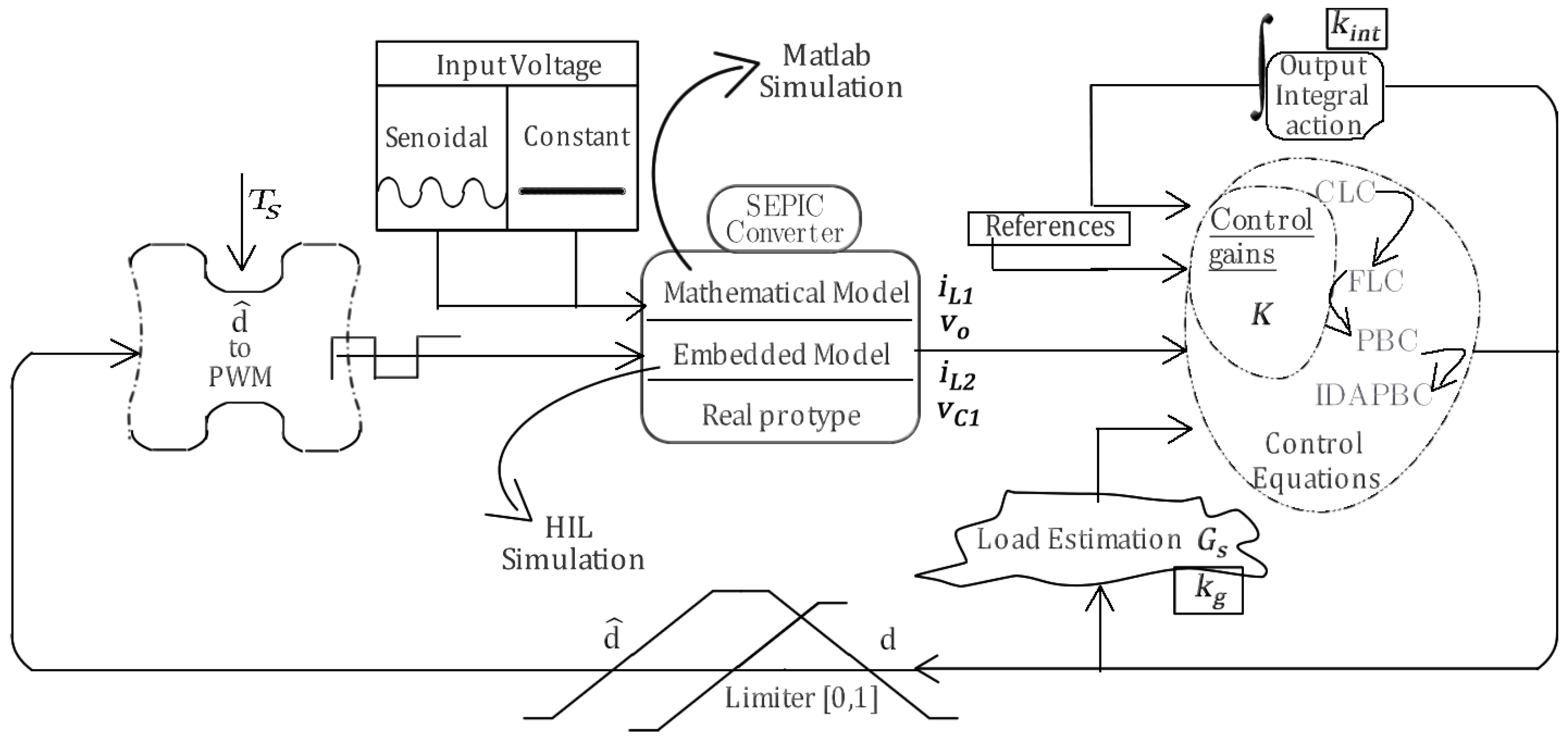
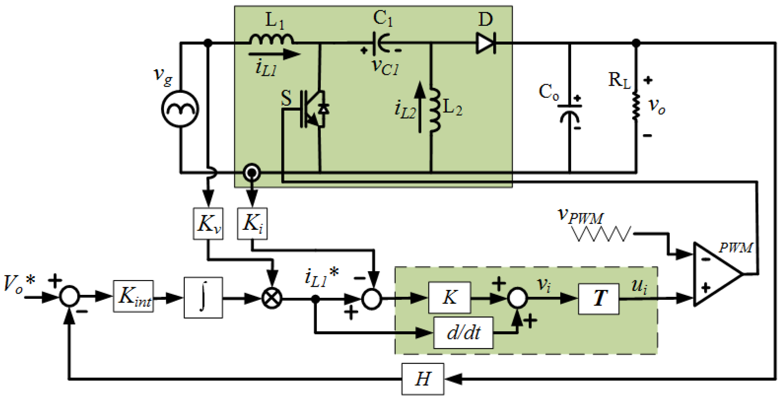
In this work, the operation characteristics, the modeling and control system of the SEPIC PFC converter in CCM and DCM are presented. Initially, a comparative analysis between two control techniques will be performed for this converter. The first one deals with the Classical Linear Control (CLC) based on the small-signal model, and the other is based on the Feedback Linearization Control (FLC) approach. Next, we suggest a new nonlinear controller, which works around the drawbacks of the CLC and FLC methods. The proposed control law, explained in the dedicated section, we call Adaptive Passivity-Based Feedback Linearization Control (APBFLC).
In order to analyze the operation of the SEPIC PFC converter, numerical simulations were performed in software for both the nominal condition and disturbances in the operation of this converter, by analyzing the Power Factor (PF) on the AC side, the harmonic distortion (THDi) of the input current and the DC side voltage regulation.
We list the main contributions of this paper:
  • a comparative analysis between linear and nonlinear control;
  • the proposal of an adaptive nonlinear control without current measurement in the intermediate inductor and with low harmonic distortion: APBFLC;
  • recent IDAPBC methods adapted from the boost converter adjusted to the SEPIC converter with very low overshoot in view of load disturbances: IDAPBC-BB;
  • HIL simulation of nonlinear control techniques applied to DC-DC SEPIC in CCM mode.
This work is organized as follows. Section 2 introduces the modeling and analysis of the converters in CCM and DCM. The description of the design and the control techniques implemented for the PFC system, as well as the control law for DC-DC are shown in Section 3. Section 4 presents the proposed APBFLC controller. Section 5 includes the adaptation of new and efficient boost control laws to SEPIC converters. Section 6 demonstrates and discusses the main simulations and the HIL experimental results. Finally, in Section 7, the final comments and conclusions are presented.

2. Modeling

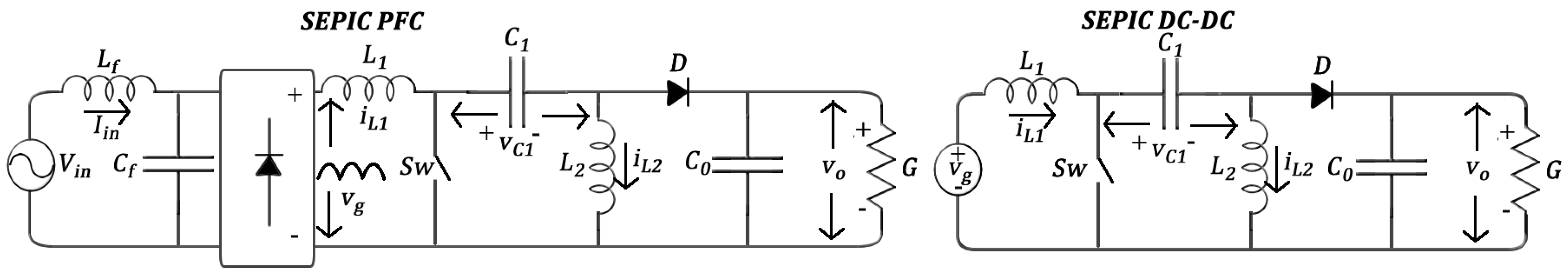
The PFC and DC-DC SEPIC converter circuits are illustrated in Figure 2. Based on [14,15], the average State-Space Model (SSM) and Euler–Lagrange Model (ELM) are presented in Table 1. Note that i L 1 and i L 2 are the average currents in the inductors L 1 and L 2 , v C 1 is the capacitor voltage C 1 , v o is the output voltage across the capacitor C o , d is duty cycle, G is the load conductance and v g is the input voltage. Note in Table 1 that the differences between the two conduction modes basically consist of the residual term presented in the states representing the inductors currents ( I s i g = 0 for CCM and I s i g 0 for DCM).

2.1. CCM and DCM Analysis

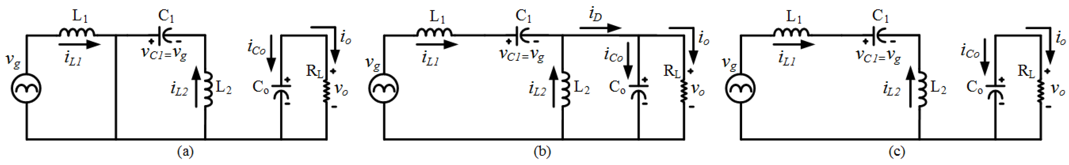
The operation details of the SEPIC converter in DCM, illustrated in Figure 3, outline three mode configurations, which depend on the states of the semiconductor switch S and the diode D. The third configuration (c) represents the discontinuous operation mode, which is characterized by the annulment of the current drained through the diode. This is due to the inversion in one of the inductor currents of the converter, which will also equal in intensity the current of the other inductor; so the sum of these currents ( i L 1 + i L 2 ) will become zero during a short time interval. If the sum of these currents is always greater than zero ( i L 1 + i L 2 ) > 0 over the entire span where the switch remains open, there will be a current across the diode, and only the configurations (a) and (b) will be observed, which will represent the operation of the converter in continuous mode.
According to [14], the operation of the SEPIC converter in DCM can be analytically represented by (1), where S Q and θ L 1 + L 2 are the switching and the threshold functions, respectively. These functions of the switch model are presented in (2) and (3), where z = i L 1 + i L 2 . In addition, S ¯ Q and are their respective complements.
L 1 d i L 1 d t = S Q · v g + S ¯ Q · θ ( z ) · ( v g v c 1 v o ) + S ¯ Q · θ ¯ ( z ) · L 1 L 1 + L 2 · ( v g v c 1 ) L 2 d i L 2 d t = S Q · v c 1 S ¯ Q · θ ( z ) · v o S ¯ Q · θ ¯ ( Q ) · L 2 L 1 + L 2 · ( v g v c 1 ) C 1 d v C 1 d t = S ¯ Q · i L 1 S Q · i L 2 C o d v o d t = S Q ¯ · θ ( z ) · ( i L 1 + i L 2 ) i o
S Q = 0 , c l o s e   s w i t c h 1 , o p e n   s w i t c h
θ ( z ) = 0 , s e   z 0 1 , s e   z > 0
Let us derive the state-space averaging approach of (1), considering the DCM SEPIC converter operation, to obtain:
L 1 d i L 1 d t = v g ( 1 d ) · ( v c 1 + v o ) + ( 1 d ) · L 1 L 1 + L 2 ( v g v c 1 ) C o d v o d t = ( 1 d ) · ( i L 1 + i L 2 ) i o L 2 d i L 2 d t = d · v c 1 ( 1 d ) . v o ( 1 d ) · L 2 L 1 + L 2 · ( v g v c 1 ) C 1 d v C 1 d t = ( 1 d ) · i L 1 d · i L 2
where d is the duty cycle of the semiconductor switch. According to [16], the average output current of the SEPIC converter in DCM for a half cycle of the AC line and the AC current grid can be written, respectively, as follows:
I o = V i n 2 D 2 T S 4 L e q v o
i i n = I i n s i n ( w t )
where L e q is the equivalent inductance derived from the parallel association of the inductors and I i n is given by:
I i n = V i n D 2 T S 2 L e q

2.2. PFC Converter Characteristics

In power factor correction applications (AC-DC), as shown in Figure 4, the input voltage and current can be described by:
v g = V i n | s i n ( w t ) |
i L 1 = I i n | s i n ( w t ) |
where V i n and I i n are the amplitude values of these input quantities and w is the angular frequency. Note that for a DC-DC system, the input v g is constant.
On the other hand, the output voltage v o remains practically constant throughout each half cycle due to the presence of the large output capacitor C o . Hence, this voltage can be approximated by a constant value v o V o .
In addition, the PFC converter operates under very special conditions where the nominal DC voltage transformation m w t and the load r w t “seen” by the converter, at each period, are given by:
m ( w t ) = v o v g V o V i n | s i n ( w t ) | = M | s i n ( w t ) |
r ( w t ) = R 2 s i n 2 ( w t )
where these quantities periodically vary from a minimum value M and R / 2 ( w t = π / 2 ) to infinity ( w t = k π , with k = 0 , 1 , 2 , 3 , ) in each half cycle of the grid frequency. Such features extend to any type of DC-DC converter used as PFC.

2.3. CIECA Modeling

The CIECA approach (Current Injected Equivalent Circuit Approach), proposed by [17], works to simplify the DCM SEPIC modeling taking into account some desired characteristics:
  • Simple, clear, works in both continuous and discontinuous conduction mode (CCM or DCM);
  • Can produce a well-suited approximated version of a real converter;
  • The equivalent circuit can be used directly in digital software simulators (SPICE, MATLAB, PSIM and others).
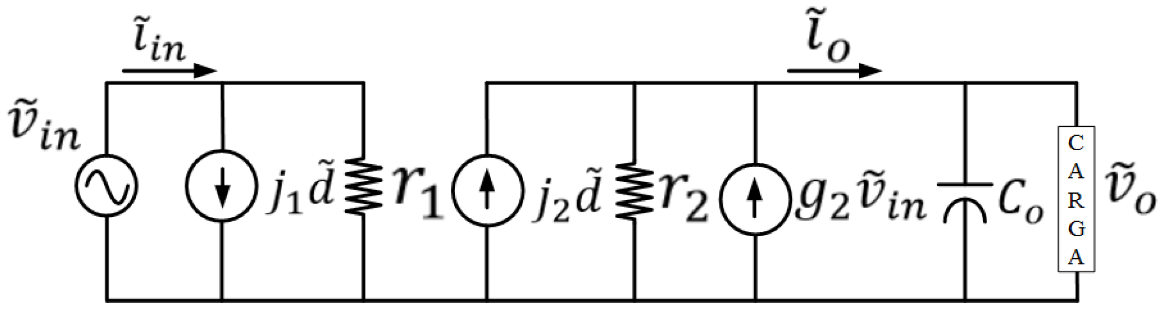
In the CIECA design procedure, the first step is to identify the nonlinear part of the converter circuit (containing the switch). The second is the linearization, which is done through the average current. This fact makes simple the application of this approach, and the final result of the modeling becomes a set of small-signal equations. Therefore, a linear equivalent circuit model for the nonlinear converter is sketched in Figure 5, representing the transfer ratios of the converter. The CIECA modeling can be applied to CLC control.
The dynamic properties of the converter are determined from an introduction of an AC small-signal variation on the steady-state operating point, where the small signal values are considered to be much smaller than the quiescent values: d = D ¯ + d ˜ , V i n = V ¯ i n + v ˜ i n , v o = V ¯ o + v ˜ o , I i n = I ¯ i n + i ˜ i n and i o = I ¯ o + i ˜ o , where “−” indicates the steady-state value and “∼” represents the small-signal disturbance introduced.
Applying these disturbances in (5), which shows the value of the output current, and upon eliminating nonlinear second-order terms, this leads to:
i ˜ o = j 2 d ˜ + g 2 v ˜ i n 1 r 2 v ˜ o
where: j 2 = V ¯ i n 2 V ¯ o D ¯ T S 2 L e q , g 2 = V ¯ i n V ¯ o D ¯ 2 T S 2 L e q and r 2 = V ¯ o I ¯ o .
Using these same perturbations in (7), we have:
i ˜ i n = j 1 d ˜ + 1 r 1 v ˜ i n
where: j 1 = V ¯ i n D ¯ T S L e q and r 1 = 2 L e q D ¯ 2 T S .
The expressions (12) and (13) represent the model of small low-frequency signals of the SEPIC converter. They are also used to obtain the equivalent small-signal circuit, illustrated in Figure 5. From this equivalent circuit, the desired transfer functions of the SEPIC converter can be obtained. In addition, it should be noted that the equivalent small signal impedance of the load ( Z l o a d ) directly depends on the load to which the PFC converter is connected. In this case, making use of a purely resistive load ( R L ), the equivalent small signal impedance shall be considered equal to the load itself, i.e., Z l o a d = R L .

3. Control System

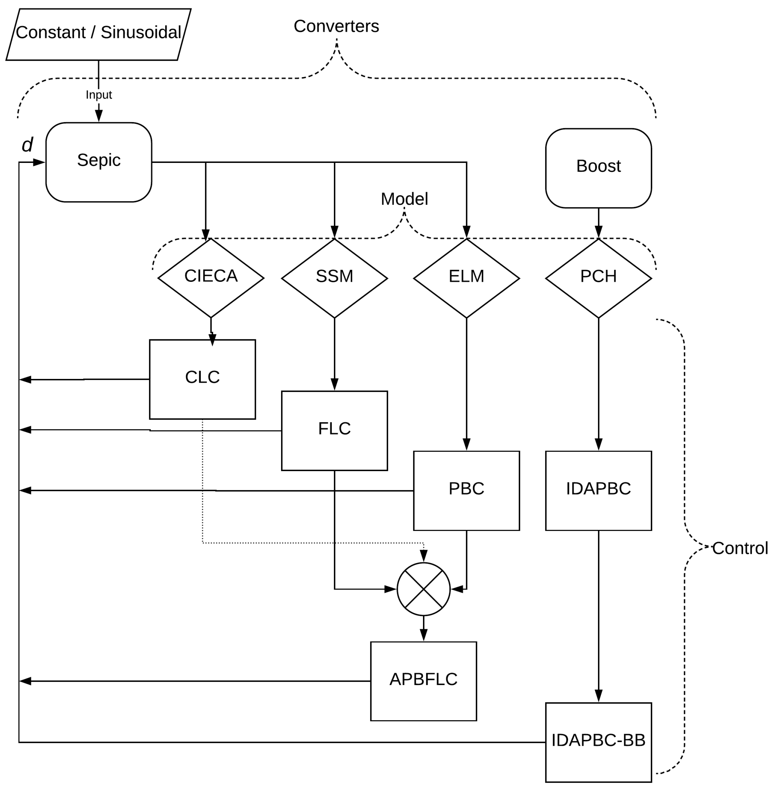
Several control techniques for switched converters are presented in the literature. In this work, an initial comparison is made between two of them: the traditional approach, using a Proportional-Integral (PI) controller and the nonlinear technique based on FLC (Feedback Linearization Control). A generalized procedure for both linear and non-linear control is shown in Figure 6. The complementary flowchart, sketched in Figure 7, outlines important observations:
  • CLC needs CIECA modeling (Section 3.1);
  • FLC and PBC employ SSM and ELM models, respectively;
  • The APBFLC control (Section 4) incorporates the advantages of FLC and PBC. The integral action used in the classical control can also be added.
  • The IDAPBC-BB control (Section 5) is obtained through the simplified modeling based on the boost converter and the IDABPBC control, which utilizes the Port-Controlled Hamiltonian (PCH) model (Appendix B);
When considering the classic control system of the PFC converters, there are two main methods: the multiplicative and the follower voltage, portrayed in [16]. In the case of SEPIC PFC in DCM mode operation, there is an inherent characteristic that simplifies and establishes the control system, explained in the following subsection.

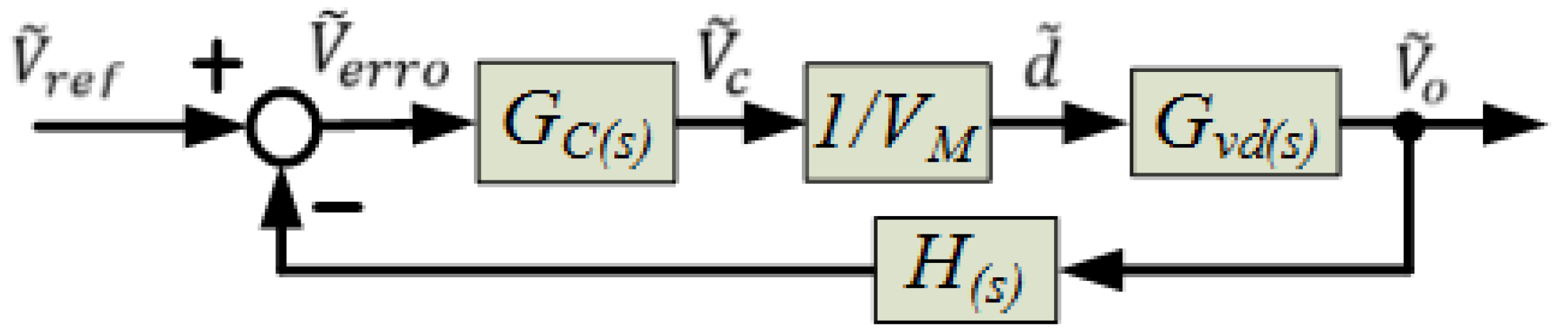
3.1. Classic Control

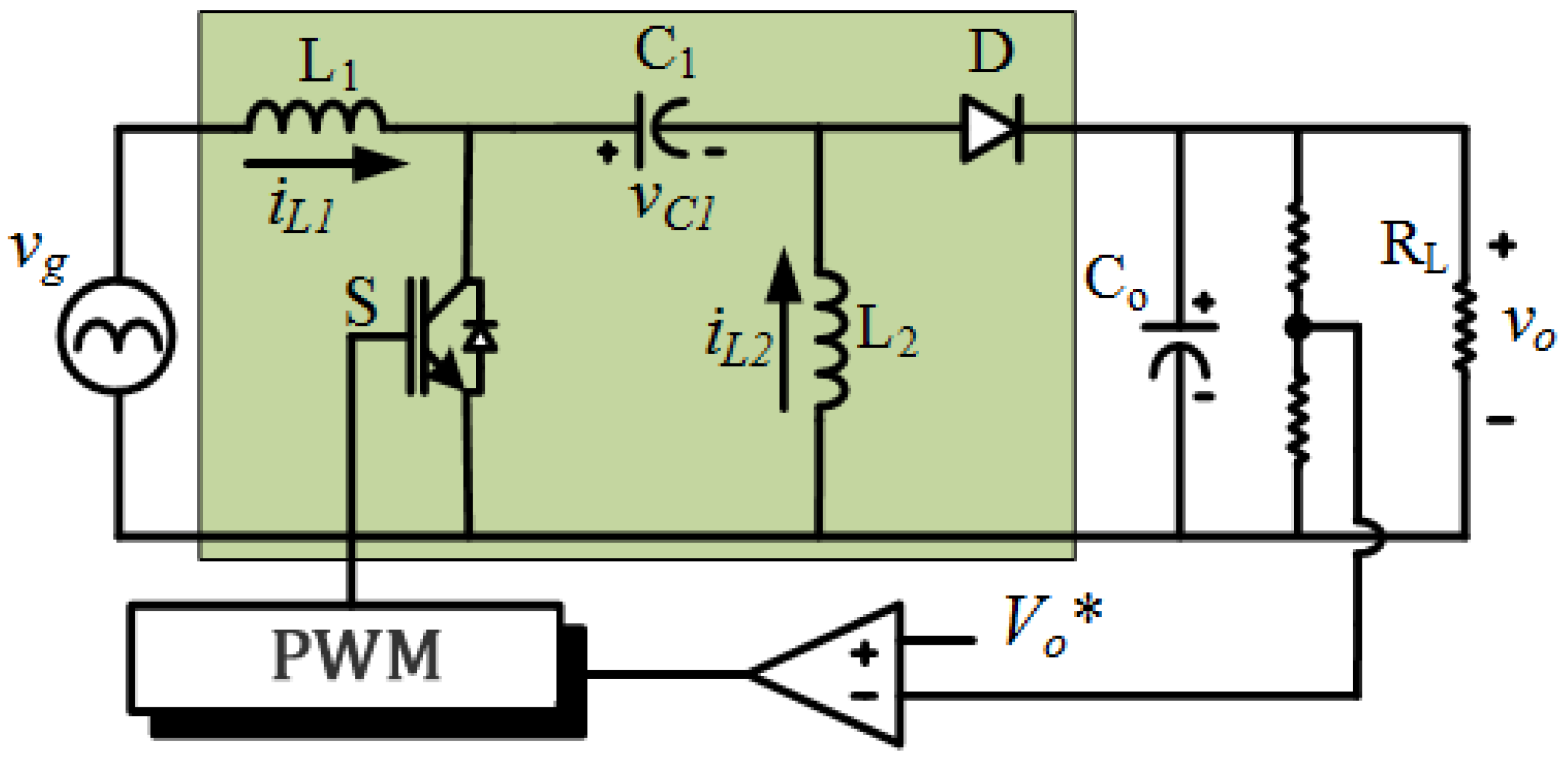
In the traditional linear approach, the control system is reduced to a single voltage loop, which is sketched in Figure 4. This control system can also be represented in the form of block diagrams of Figure 8, where the SEPIC converter and the PWM controller (Pulse-Width Modulation) are replaced by their respective transfer functions: G v d ( s ) and G C ( s ) . The other elements correspond to the amplitude of the triangular wave V M and voltage sensor gain H ( s ) .
The voltage-proportional-integral PWM controller is designed using the classical frequency domain technique presented in [18]. The transfer function G v d ( s ) relates the output voltage to the duty cycle, obtained from the small-signal equivalent circuit of the Figure 5, as follows:
G v d ( s ) = j 2 C o s + 1 r 2 + 1 R L
In addition, this classical PI controller adjustment is based on the definition of the transfer function T ( s ) , which is given by:
T ( s ) = H ( s ) G C ( s ) G v d ( s ) / V M

3.2. Feedback Linearization Control

In the case of the FLC technique, there is a linearization of the nonlinear dynamics of the system by state feedback, which is applied to the entire domain of the state space except for some singular points, so, it is global. Thus, this approach differs from linearization in the neighborhood of an equilibrium point, which was used to construct the equivalent model of Figure 5.
The design of the control system in the FLC approach is performed including a variable change, which shows the structure of the designed controller [14]. In addition, the control law is based on the knowledge of the average converter model, which was presented in (4). In relation to this model, it is observed that the system presents a unity relative degree. This fact makes possible the derivation of the current control law from the first equation of this average model:
d = ( L 1 v i v g ) ( L 1 + L 2 ) ( L 1 + L 2 ) ( v c 1 + V o ) + L 1 ( v c 1 v g ) + 1
which:
d = 1 2 1 + u i V M
where u i is the output of the FLC controller, V M corresponds to the amplitude of the triangular wave and v i is the new variable, given by:
v i = i L 1 * d t K L 1 ( i L 1 i L 1 * )
In turn, the reference current i L 1 * , whose amplitude was defined in (7), is represented by:
i L 1 * = I i n | s i n ( w t ) |
In addition, due to possible regime errors caused by the parametric uncertainties and in order to regulate the output voltage at the desired value V o * , it is necessary to introduce an integral action, which is represented as follows:
V o = K i n t 0 t v o V o * d t
Finally, Figure 9 shows the control system in the FLC approach, where the function T represents the relation between the auxiliary variable v i and the controller output u i . Such a function can be obtained by solving the expressions (16)–(18). FLC and PBC control equations for CCM and DCM SEPIC are summarized in Table 3. Note that PBC has the same first Equation (16) and three morestate equations.

3.3. Numerical and Initial Implementations for SEPIC DCM PFC

The reactive power elements of SEPIC is presented in Appendix A. An important quantity to be calculated is the transfer function G v d ( s ) shown in (14), which is given numerically by:
G v d ( s ) = 400 0.016 S + 1
where: j 2 = 8.06 and r 2 = 99.20 .
This transfer function has great importance for the control loop adjustment in the classical approach, which must be sufficiently slow in order to avoid the injection of the second harmonic of the output in the input current. In this case, an expressive third order harmonic component can appear. As suggested in [19,20], it is necessary to allocate the crossover frequency of the control at least three times less than the AC input frequency, which makes the control system naturally slow.
Again, the PI controller was tuned using the classical frequency domain technique. The characteristics of this control system are shown in Table 2 together with the FLC control parameters. The next step is to analyze the AC side Power Factor (PF), the Total Harmonic Distortion of the input current (THDi) and the DC side voltage regulation in the simulated system for both the nominal condition and operation disturbances.
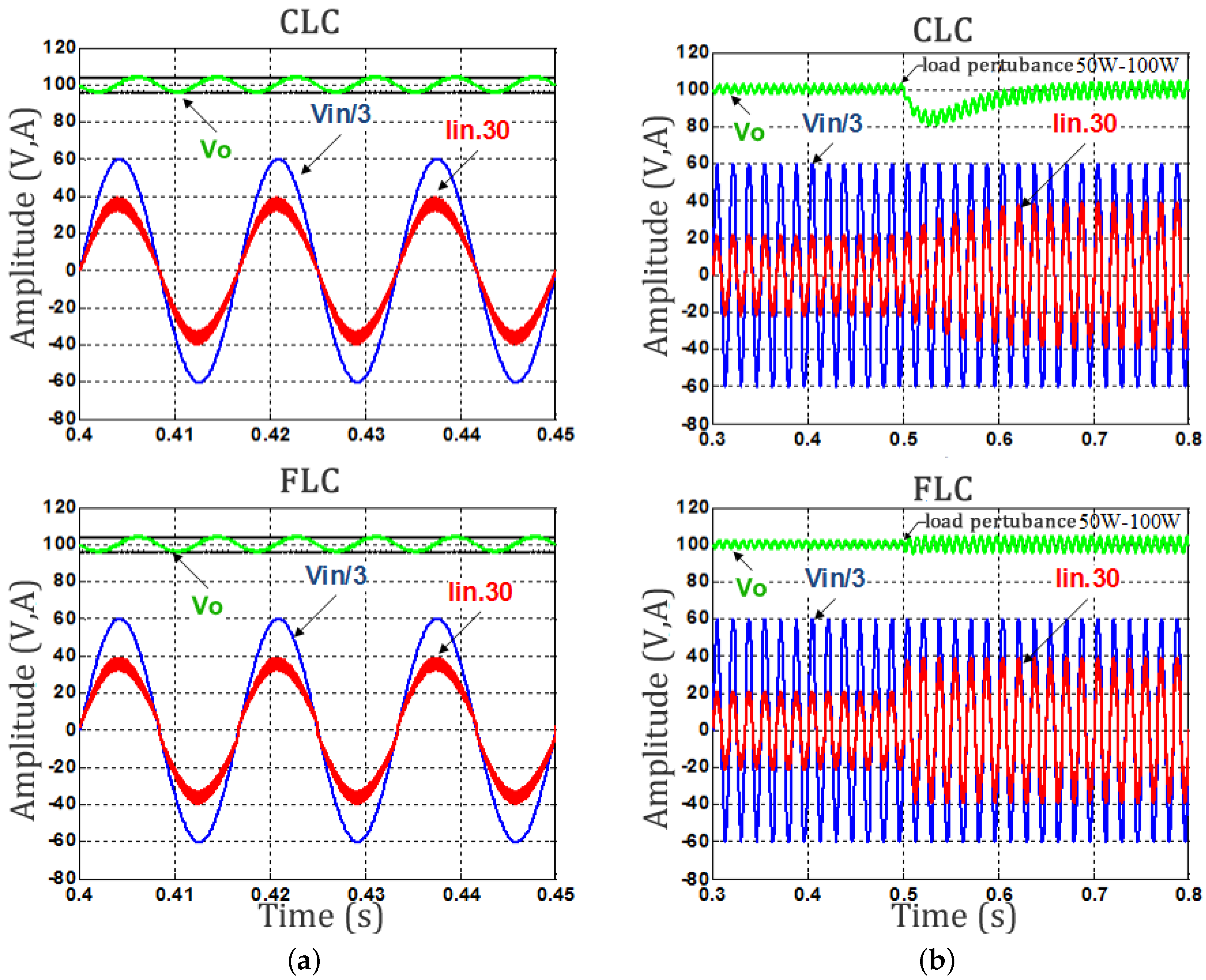
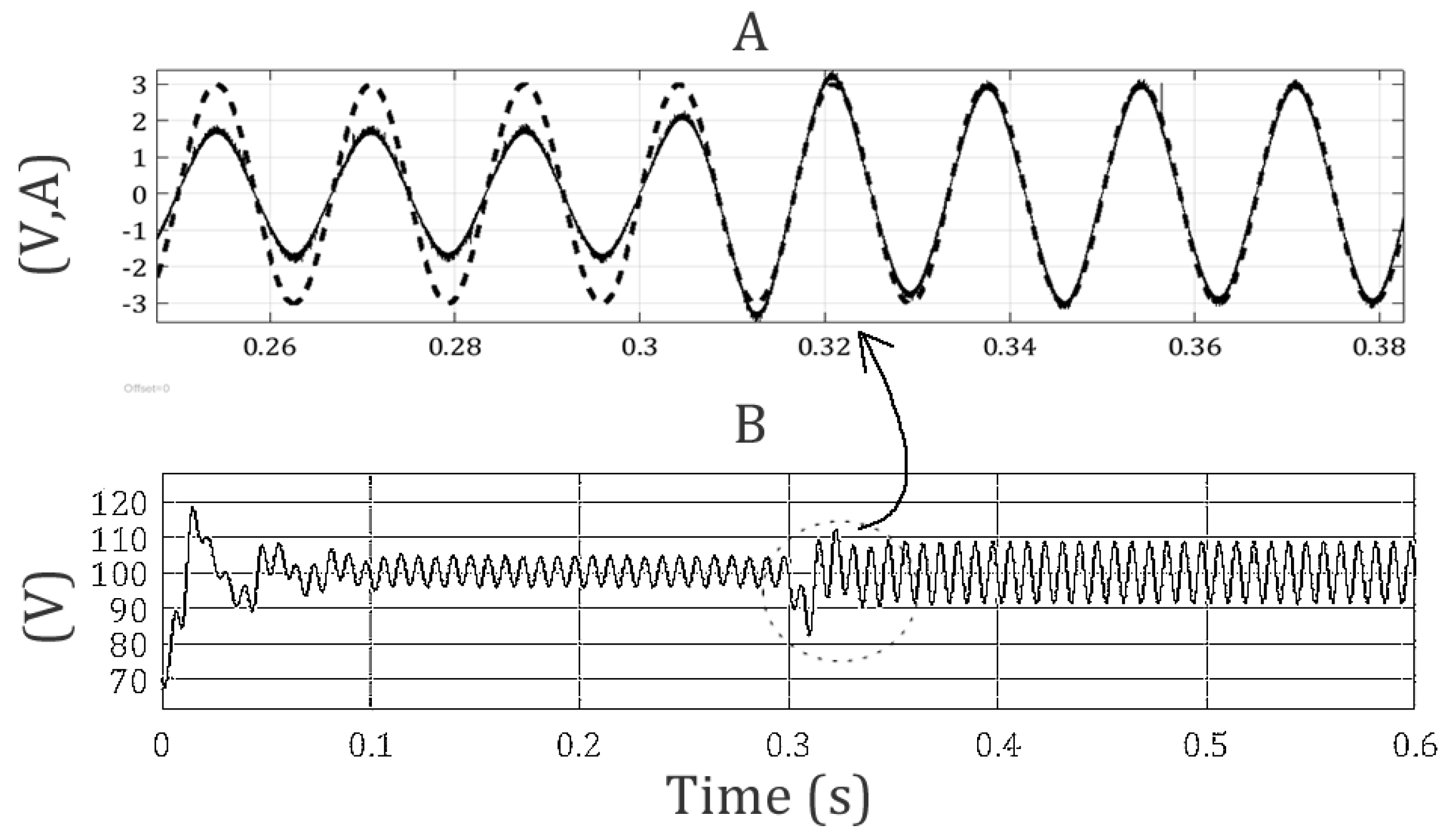
The first analysis considers the operation of the full load converter (100 W), as shown in Figure 10a. In this figure, it is possible to observe the power factor correction characteristic of the SEPIC PFC converter, which has a high power factor ( L i n e a r —0.9975, F L C —0.9971), low harmonic content ( L i n e a r —6.33%; F L C 
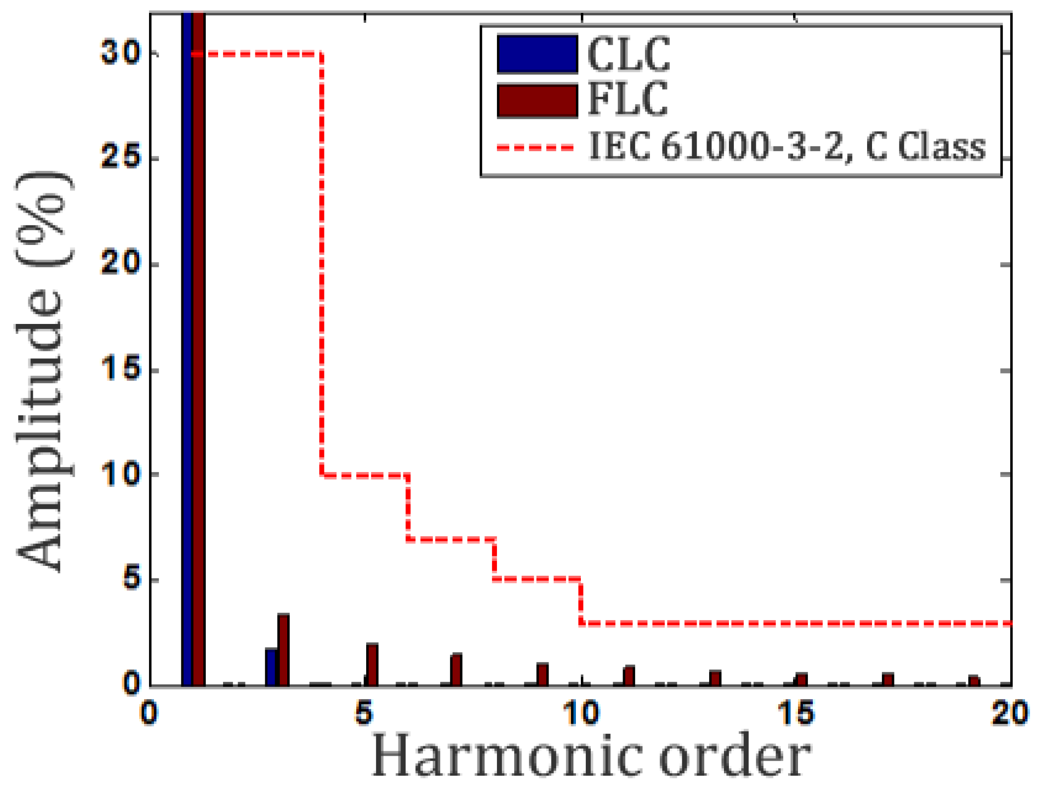
—7.60%) and is still able to maintain the output voltage at the reference of 100 V within the limits imposed by the design. The low harmonic content of the input current is evidenced in the spectral analysis shown in Figure 11, where it is noted that the values obtained in the two control approaches are far below the limits imposed by the IEC 61000-3-2, Standard Class C.
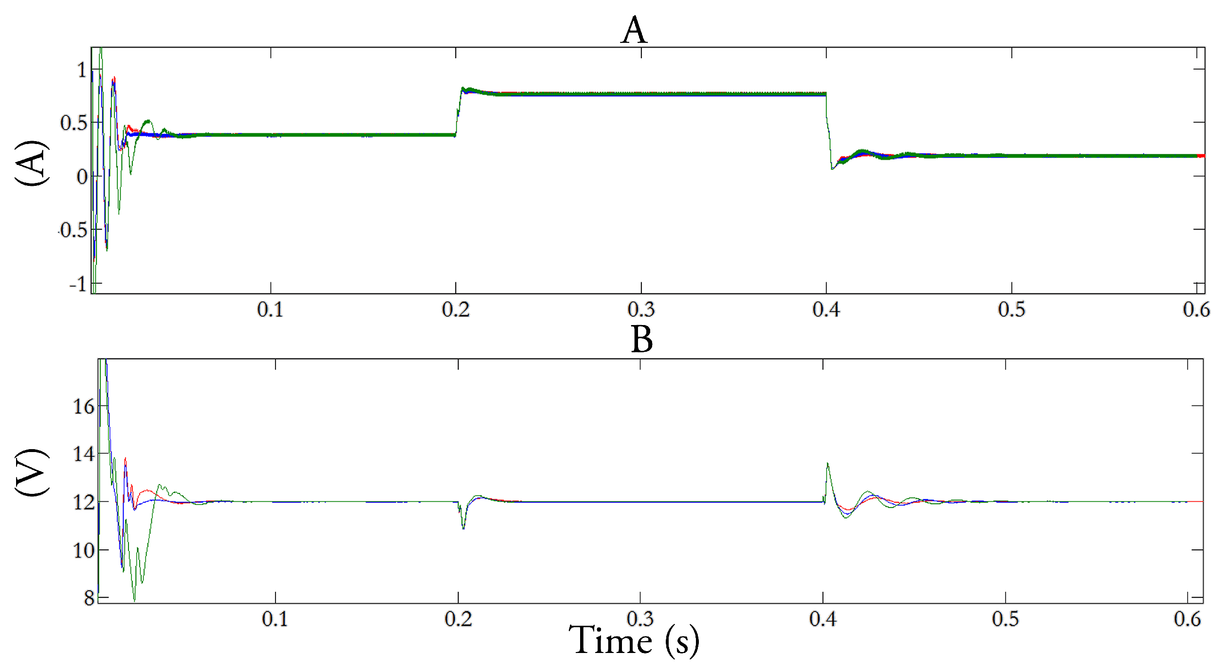
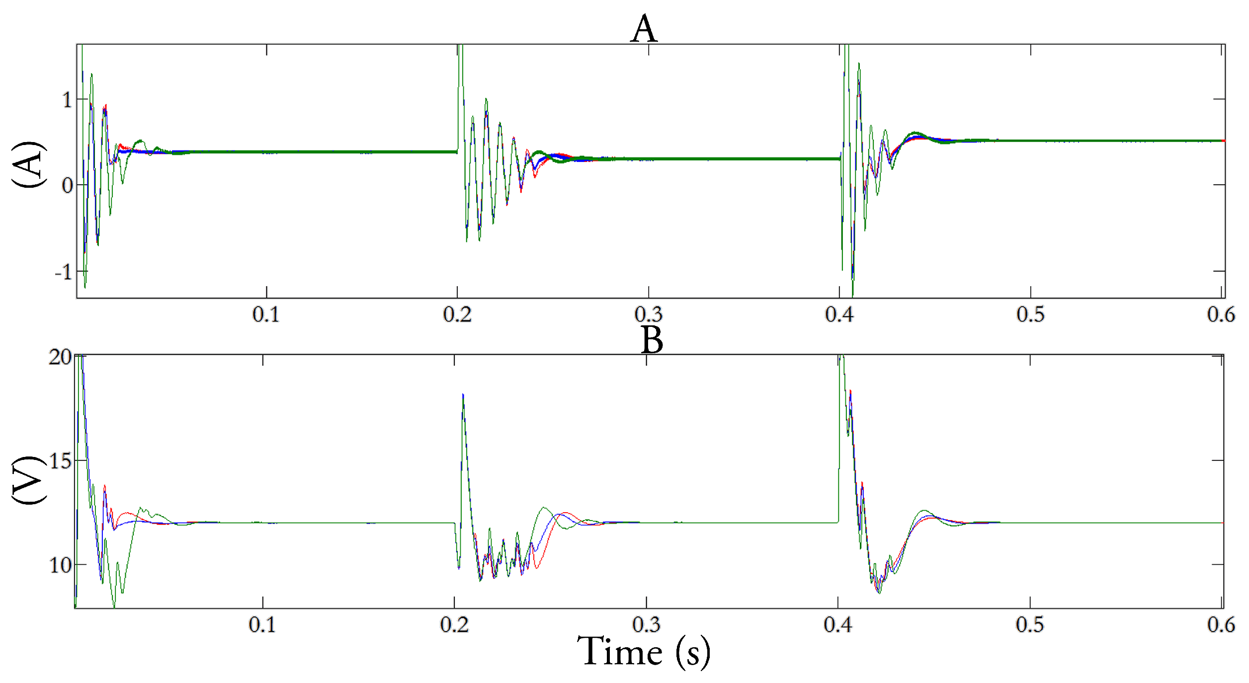
It can be seen from Figure 10b that the dynamic behavior of the SEPIC converter is able to regulate the output voltage in both control strategies, although it takes different times to achieve this regulation, for a load variation of 50 W–100 W. In the case of the linear approach, the SEPIC converter spends approximately 120 ms to perform the voltage regulation, allowing that voltage to decrease by approximately 20 V. On the other hand, the converter has been able to regulate this output voltage in less than one grid cycle in the FLC approach. In addition, in the nonlinear technique, an overvoltage or current signal is not verified in the voltage regulation, surpassing the linear approach in this discussion point.
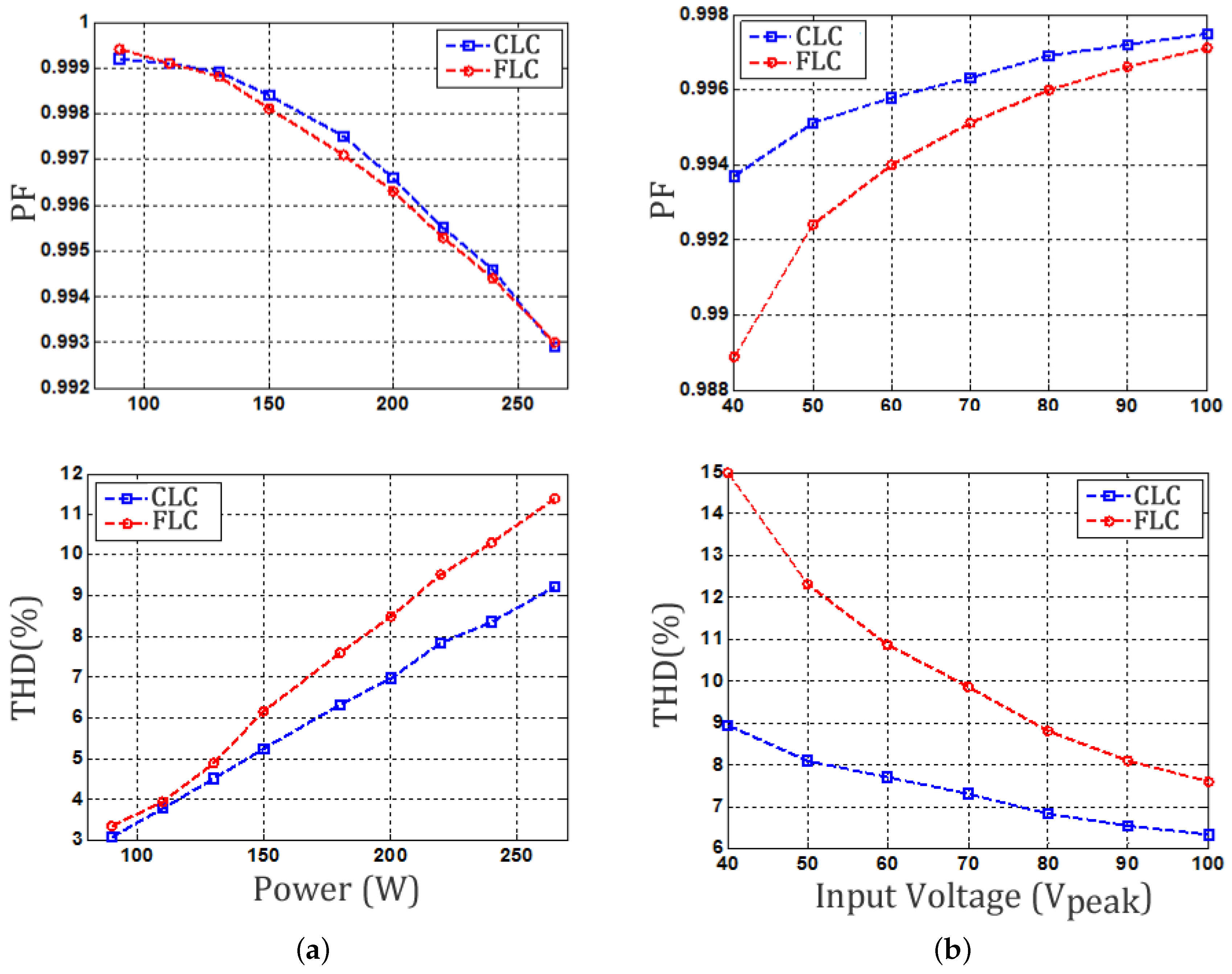
Finally, an analysis of the power factor and harmonic distortion of the AC input current is performed for both the universal input voltage values (90–265 V peak) at full load (100 W) and for different values of the load connected to the SEPIC converter. The first one is presented in Figure 12a and shows that the converter has a high power factor and low harmonic content in the AC current along the entire voltage range of the universal input in both methods. However, it is noted that the linear technique presents a slight superiority in this test.
The other analysis is presented in Figure 12b, and again, the converter is able to maintain a high power factor and low harmonic content in both control approaches, now for different load values. In addition, it is observed that there is a more evident superiority of the linear approach in this last analysis to the different values of the load, which can be explained by the distortion in the waveform of the current in the passage through zero due to the presence of a derivative action in the FLC methodology.

4. Proposed Adaptive Non Linear Control Law

The two control laws discussed above, both linear and non-linear, have some drawbacks, which will be discussed below. First, for the classic controller shown in Figure 7, the control structure directly depends on the output signal of a voltage error amplifier (which contains a second harmonic component) and the input rectified sine wave voltage. As explained in [20], the linear controller ends up leading to higher levels in the third harmonic of the input current. To minimize this aggravating factor, the control loop is intentionally slow. The other disadvantage is the restriction at the operation point of the system since linearization is local around the equilibrium point. It should also be added that linear control works for DCM mode; the same performance does not occur in CCM mode.
The FLC control presents a major practical implementation problem: it needs the known value of the load G. Note that (7) depends on the desired current value in the primary inductor, which in turn depends on the value of G. Figure 11 shows this deficiency in the FLC control. In view of these two major disadvantages, we propose the following adaptive control law based on the passivity-based control and feedback linearization control Table 3, which we call APBFLC.
v i = i L 1 * d t K 1 L 1 ( i L 1 i L 1 * ) ,
D C M : d = ( L 1 v i v g ) ( L 1 + L 2 ) ( L 1 + L 2 ) ( v c 1 + v o * ) + L 1 ( v c 1 v g ) + 1 ,
C C M : d = L 1 v i + v o * + v c 1 v g v o * + v c 1 ,
v o * ˙ = 1 C o ( 1 d ) ( i L 1 * + i L 2 * ) G v o * + k 2 ( v o v o * ) ,
i L 1 * = I i n | s i n ( w t ) | ,
i L 2 * = v g V o * I i n | s i n ( w t ) | ,
G = G s .
When the load is unknown, although constant, an adaptive control strategy, as presented in [21], can be applied, where the unknown load conductance is adapted as follows:
G s = k g v o * 0 t [ v o ( s ) v o * ( s ) ] d s .
For a DC-DC system:
i L 1 * d t = 0 , i L 1 * = G v g V o * 2 ,
i L 2 * = G V o * .
Note that it is necessary to estimate an additional state: the output voltage v o given by (23). The integral action, given by (20), can also be included in the control law. We list the following advantages of the proposed law:
  • In contrast to the classical control, it gives an indirect and less dependent control of the 120-Hz ripple output voltage, which, therefore, allows for lower THDi levels; a higher phase margin due to non-restriction operating point. The integral gain can be stipulated for a faster response.
  • Complements the FLC control and allows load estimation given by (26), being more robust to load disturbances;
  • Given the caveats imposed by (22), the adaptive control law works for both conduction current modes (DCM and CCM);
  • Neglecting the current measurement of the intermediate inductor L 2 ; this characteristic is motivated by the analysis discussed in the following section.

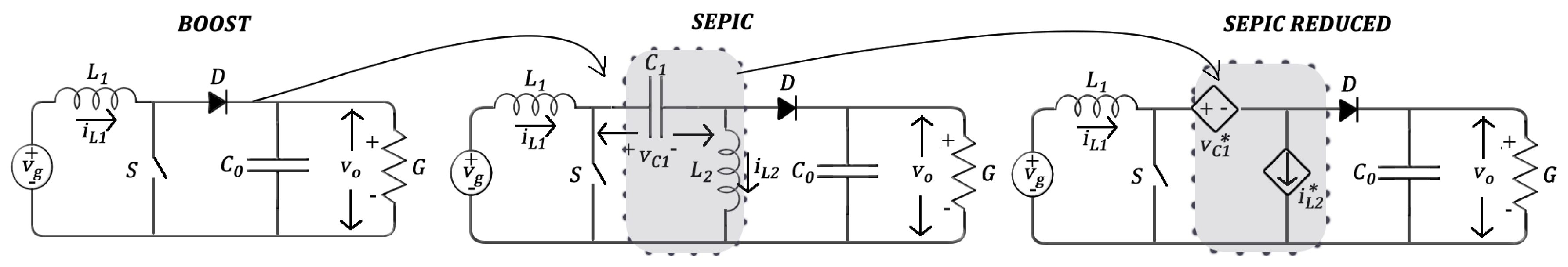
5. Revised SEPIC as a Boost Converter and Derived Equations

The SEPIC converter has two inductors and two capacitors (a fourth order system), so it is necessary to reduce the number of states and measurements, for cost and error propagation reasons. In view of this concern, Ref. [15,22] use observers and immersion techniques. In [23], the fourth order transfer function of SEPIC is reduced to second order using the Pade approximation method, where the designed compensator closely follows the original system’s response. Furthermore, Ref. [24] employ a simplified second order state-averaged model, using the sliding surface-regulated current-mode PWM controller. In addition, the CIECA modeling discussed in Section 2.3 motivates an interesting question: Is it possible to reduce the states of the SEPIC converter, for example, considering only the output voltage and the input current?
In Figure 13, the boost and SEPIC converters are placed side by side for comparison. It is observed that when removing the intermediate elements ( L 2 , C 1 ) highlighted by the dotted line, the SEPIC converter becomes similar to the boost converter, having similar equilibrium points as shown in Table 4. This is the reason that these converters are recommended to work in PFC systems. What is the advantage of this adaptation?
Therefore, we can use the boost equations and apply them to control the SEPIC converter replacing the state variables eliminated ( i L 2 and v c 1 ) by the equilibrium points, provided in Table 4, represented by dependent sources in the model. If we substitute, for example, v c 1 by v g and i L 2 by G V o * in the SEPIC converter, it saves two sensors. Figure 13 summarizes this process. The other option is to replace the desired state reference by the measurement of the state itself, as seen in (23).
To illustrate an example application, we consider two control laws based on IDAPBC. In [22], IDAPBC control is applied to boost converters achieving an effortless and open loop control equation:
IDAPBC-1:
d ¯ = 1 v g V o * , d = 1 1 d ¯ v o V o * k α
Yet, Ref. [25] proposed an evolution of (28) given by:
IDAPBC-2:
d = 1 k z v g 2 v g v o + ( k z 2 v o ) V o *
Equations (28) and (29) can be applied to SEPIC converters, which we denominate as IDAPBC-BB control equations. Again, the integral action, given by (20), can also be added. In order to illustrate how to insert this term in the control law, just replace the desired variable in the output voltage ( V o * ) by the integral of the error between the measured variable ( v o ) and the reference constant value ( V o * ). Thus, the new control law becomes:
d = 1 k z v g 2 v g v o + ( k z 2 v o ) V o ( i n t ) * ,
V o ( i n t ) * = k i n t 0 t [ v o ( s ) V o * ] d s
The boost IDAPBC control equations are presented in Appendix B.

6. Main Results

In order to verify the performance of the control systems applied to the SEPIC DC-DC CCM and SEPIC PFC DCM, software and HIL simulations were performed using the specifications presented in Table 5.

6.1. SEPIC DC-DC CCM and HIL Simulation Results

This section presents the digital simulation results using MATLAB and Hardware in the Loop (HIL) procedure described in [26]. The converter is implemented according to the design specifications of Table 5 and the three control laws: FLC, APBFLC and IDAPBC-BB.
Figure 14 shows the capacitor voltage and inductor current response for load perturbation, respectively, in the SEPIC converter simulated in software. In the same way, Figure 15 presents the voltage and current response to an input voltage variation. In both input and load variation, consecutive steps of 50–100% are applied in the simulated systems. Figure 16 shows the out capacitor voltage of SEPIC converter, respectively, for the HIL application.
As seen in Figure 14, Figure 15 and Figure 16, both software simulations and HIL results converged to the steady state value after the consecutive step applications. It is notable that the behavior of the systems are compatible, since the same transient dynamics is seen, even for the IDA-PBC’s oscillatory dynamics. None of the implemented systems in software or in HIL converged to instability. This means that the embedded models and control equations are capable of controlling the systems, so validating the control techniques.
The processing time for the DSP to compute the control law and therefore to run a real-time simulation is 1.2 µs. Using a switching frequency of 50 kHz (20 µs), the processing time of all control equations (1.2 µs) demands 6% of the bandwidth.

6.2. APBFLC Results

As sketched in Figure 17, the output voltage can asymptotically track the set-point even if the load perturbation is present. The APBFLC controller features low THDi (<2%), low overshoot (<10%) and fast response speed (<0.05 s). The power factor achieved for the nominal condition is PF = 0.99.

6.3. IDAPBC-BB Results

Next, the two control laws (28) and (29) are validated in simulation. We can again observe the stability of the adapted nonlinear controllers by analyzing the change in perturbation of the output voltage waveform over a load step (note the insignificant overshoot of IDAPBC-BB-2 response). Hence, this variable is controlled at the desired value V o * . The steady-state and perturbed waveforms are sketched in Figure 18 showing that the two methods have low overshoot and fast response, even considering a control law adapted from the boost converter, taking into account only the measurement of the output voltage.

7. Conclusions

The intrinsic power factor correction includes SEPIC in a particular group of converters. Hence, the design of the control system derived from the model based on CIECA and the boost converter is satisfactory, revealing that it is possible to obtain high performance controllers using a simplified modeling. In addition, the effectiveness of the nonlinear approaches was verified, whose control laws proved to be efficient, especially for the voltage regulation and transient dynamics.
The performance of the proposed nonlinear controllers was analyzed under variations in load and input voltage. The software and HIL simulations demonstrated the feasibility of the nonlinear algorithms that can be used in embedded systems and practical applications, with simplicity and high accuracy.
Thus, we recommend:
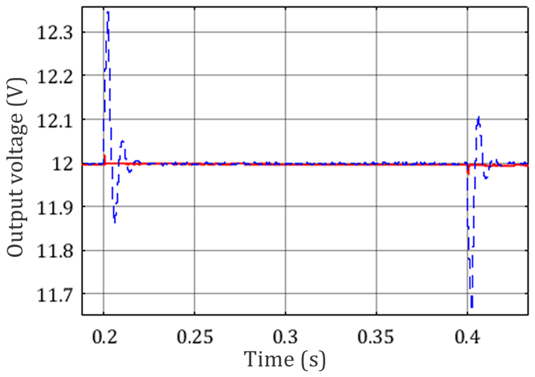
  • For DC-DC SEPIC: the IDAPBC-BB-2 controller, because it presents ultra-low overshoot and ultra-fast response speed; all these benefits are sufficiently attained using only one measure (output voltage v o );
  • For PFC SEPIC: the APBFLC control method, which offers high robustness, low THDi, low overshoot, load estimation possibility and fast response; all these advantages were achieved regardless of mode operation (CCM or DCM).

Acknowledgments

This work has been supported by the Brazilian agencies CAPES and FAPEMIG.

Author Contributions

A.H.R.R., L.M.F.M. and S.I.S.J. conceived and designed the experiments; A.H.R.R., T.M.d.S. and. L.M.F.M. performed the experiments; A.H.R.R., T.M.d.S., L.M.F.M. and S.I.S.J. analyzed the data; A.H.R.R., L.M.F.M. and S.I.S.J. contributed materials/analysis tools; A.H.R.R. and T.M.S. wrote the paper.

Conflicts of Interest

The authors declare no conflict of interest.

Abbreviations

The following abbreviations are used in this manuscript:
ACAlternating Current
DCDirect Current
CCMContinuous Conduction Mode
CIECACurrent Injected Equivalent Circuit Approach
DCMDiscontinuous Conduction Mode
ELMEuler–Lagrange Model
FLCFeedback Linearization Control
PBCPassivity-Based Control
IDAPBCInterconnection and Damping Assignment Passivity-Based Control
IDAPBC-BBInterconnection and Damping Assignment Passivity-Based Control—Based on the Boost Converter
PCHPort-Controlled Hamiltonian
SSMState-Space Model

Nomenclature

vgInput voltage
dDuty cycle
iL1Inductor L 1 current
iL2Inductor L 2 current
voCapacitor voltage
ioOutput load current
L1Primary-side inductance
L2Secondary-side inductance
CoOutput capacitance
GLoad conductance
RLLoad resistance

Appendix A. Reactive Elements of Power Circuits

The choice of the power circuit reactive elements of the SEPIC PFC converter in DCM, discussed in this work, is directly influenced by the operation mode of this converter. Based on the work of [16], these design specification are calculated, as seen in Table A1.
Table A1. Design specifications.
ParametersValueUnity
Input voltage ( v i n )127 V R M S
Frequency (f)60Hz
Nominal power ( P n o m )100W
Output voltage ( V o )100V
Resistive load ( R L )100 Ω
Switch frequency ( f s )50kHz
Inductors ( L 1 / L 2 )4/100mH/µH
Capacitors ( C 1 / C o )470/330nF/µF
Thus, the DCM operation requires:
D < M M + 1
Note that in Figure 3, the average current in the load can be represented by the ratio of the output voltage v o and the load impedance R L . However, the amplitude of this current was previously defined in (5). Therefore, the nominal duty cycle can now be calculated as:
D = 2 M K a
where K a is the parameter given by:
K a = 2 L e q R L T S
At this discussion point, from the results presented in (A1) and (A2), it is necessary to establish a critical parameter, which will define the operating modes of the PFC SEPIC, in terms of the ratio M. Hence, we have:
K c r i t = 1 2 ( M + 1 ) 2
Note that the DCM operation requires K a < K c r i t .
Next, the inductor parameters L 1 and L 2 are calculated in view of the L 1 current ripple term:
i r i p = v g D T S L 1
Therefore, considering the worst case i r i p ( w t = 90°), the L 1 value is defined by evaluation of (A5) and the specification of the maximum admissible ripple I r i p :
L 1 = V i n D T S I r i p
Use of Equations (A6) and (7) leads to:
L 2 = L 1 L e q L 1 L e q
Finally, the value of the intermediate capacitor C 1 , which strongly influences the input current waveform of the SEPIC PFC converter, will be calculated. According to [16], a good choice is:
C 1 = 1 w r 2 ( L 1 + L 2 )
where w r is the angular frequency of C 1 , L 1 and L 2 , generally allocated between the angular frequency of the ac w and switching frequency w s , that is w < < w r < < w s .

Appendix B. IDA-PBC Control for Boost Converter

The average boost converter circuit can be written by Euler–Lagrange equations, as:
D B x ˙ + ( 1 d ) J B x + R B x = F ,
with:
x = x ˙ 1 x ˙ 2 = i ˙ L 1 v ˙ c o , D B = L 0 0 C , R B = 0 0 0 G , F = v g 0 , J B = 0 1 1 0 .
The equivalent state space equations are:
x ˙ 1 = 1 d 1 L x 2 + v g L ,
x ˙ 2 = ( 1 d ) 1 C x 1 G C x 2 ,
The modeling and IDA-PBC control of the boost converter are presented in [22]. Consecutively, the Port-Controlled Hamiltonian model (PCH) can be rearranged by the ELM to obtain:
x = x 1 x 2 , H ( x ) = 1 2 L x 1 2 + 1 2 C x 2 2 ,
J H = 0 1 d L C 1 d L C 0 , R H = 0 0 0 1 R C 2 , g H = 1 L 0 ,
x ˙ = J H d R H H z z + g H v g
The equilibrium points obtained when x ˙ 1 = 0 and x ˙ 2 = 0 in Equations (A11) and (A12) are:
x ¯ 1 = v g G ( 1 d ) 2
x ¯ 2 = v g ( 1 d )
By the equation, d as a constant value in (A14), (A15) and d ¯ , as an equilibrium value, this leads to:
x ¯ 1 = G v g x ¯ 2 2
Let us now consider the desired output capacitor voltage as x 2 d = x ¯ 2 = V o * , the equilibrium point to stabilize x ¯ and the constant input control d ¯ given by:
d ¯ = 1 E V o * , x ¯ = x 1 ¯ , x 2 ¯ T = G V o * V o * E , V o * T .
The main objective of IDA-PCB control is to find a static function through space state feedback, d = ν ( x ) . Thus, the closed loop dynamics becomes a Port-Controlled Hamiltonian (PCH), given by:
x ˙ = J d ( x , d ) R d H d x x
where the new function H d has a local minimum at the desired equilibrium point, x ¯ . The terms J d x , ν x = J d T x , ν x and R d x = R d T x 0 are the desired interconnection and damping matrices, respectively. Now, given the system:
x ˙ = J H x , d R H δ H δ x x + g H x , d
Taking into account the damping term R a H , given by:
R a H = R a H 0 0 G
this leads to the following matrix:
R d = R a H 0 0 0 .
Substituting R a H in (A18), (A19) and assuming d = ν x 2 and J H ν x R d invertible, the gain control vector K is obtained:
K = K 1 K 2 = G L x 2 1 ν x 2 C G G R a H L 2 x 1 + v g 1 ν x 2 G R a H L 2 C x 2 1 ν x 2 2
The sufficient and necessary condition for making the K vector a gradient of a scalar function is:
K 2 x 1 ( x ) = K 1 x 2 ( x ) .
Then, this condition is reduced to a simple Ordinary Differential Equation (ODE):
x 2 1 ν x 2 ν x 2 x 2 = 1 L C R a H R
which can be easily solved through the variable separation method, leading to:
d = 1 c 1 z 2 α , α = 1 L C R a H R .
The constant c 1 is chosen in such a way so as to ensure the equilibrium form:
H d x x ¯ = H x x ¯ = H a x x ¯ = 0
which implies:
c 1 = ( 1 d ¯ ) V o * α
and the IDA-PBC control equation:
d = 1 1 d ¯ x 2 V o * α .
Substituting (A17) in (A28) derives:
d = 1 v g V o * x 2 V o * α .

References

  1. Abidin, M.N.Z. IEC 61000-3-2 Harmonics Standards Overview; Schaffner EMC Inc.: Edsion, NJ, USA, 2006. [Google Scholar]
  2. Liu, Y.; Sun, Y.; Su, M. A Control Method for Bridgeless Cuk/Sepic PFC Rectifier to Achieve Power Decoupling. IEEE Trans. Ind. Electron. 2017, 64, 7272–7276. [Google Scholar] [CrossRef]
  3. Huang, L.; Chen, F.; Yao, W.; Lu, Z. Flexible Mode Bridgeless Boost PFC Rectifier with High Efficiency over a Wide Range of Input Voltage. IEEE Trans. Power Electron. 2017, 32, 3513–3524. [Google Scholar] [CrossRef]
  4. Youn, H.; Park, J.; Park, K.; Baek, J.; Moon, G. A digital predictive peak current control for power factor correction with low-input current distortion. IEEE Trans. Power Electron. 2016, 31, 900–912. [Google Scholar] [CrossRef]
  5. Kim, Y.; Sung, W.; Lee, B. Comparative performance analysis of high density and efficiency PFC topologies. IEEE Trans. Power Electron. 2014, 29, 2666–2679. [Google Scholar] [CrossRef]
  6. Moradpour, R.; Ardi, H.; Tavakoli, A. Design and Implementation of a New SEPIC-Based High Step-up DC/DC Converter for Renewable Energy Applications. IEEE Trans. Ind. Electron. 2018, 85, 1290–1297. [Google Scholar] [CrossRef]
  7. Wang, Y.; Qi, N.; Guan, Y.; Cecati, C.; Xu, D. A Single-Stage LED Driver Based on SEPIC and LLC Circuits. IEEE Trans. Ind. Electron. 2017, 64, 5766–5776. [Google Scholar] [CrossRef]
  8. Poorali, B.; Adib, E. Analysis of the integrated SEPIC-flyback converter as a single-stage single-switch power-factor-correction LED driver. IEEE Trans. Ind. Electron. 2016, 63, 3562–3570. [Google Scholar] [CrossRef]
  9. Al-Saffar, M.; Ismail, E. A high voltage ratio and low stress DC–DC converter with reduced input current ripple for fuel cell source. Renew. Energy 2015, 82, 35–43. [Google Scholar] [CrossRef]
  10. Shi, C.; Khaligh, A.; Wang, H. Interleaved SEPIC Power Factor Preregulator Using Coupled Inductors in Discontinuous Conduction Mode with Wide Output Voltage. IEEE Trans. Ind. Appl. 2016, 52, 3461–3471. [Google Scholar] [CrossRef]
  11. Sabzali, A.; Ismail, E.H.; Behbehani, H. High voltage step-up integrated double Boost–Sepic DC–DC converter for fuel-cell and photovoltaic applications. Renew. Energy 2015, 82, 44–53. [Google Scholar] [CrossRef]
  12. Kumar, K.; Babu, N.R.; Prabhu, K. Design and Analysis of an Integrated Cuk-SEPIC Converter with MPPT for Standalone Wind/PV Hybrid System. Int. J. Renew. Energy Res. 2017, 7, 96–106. [Google Scholar]
  13. Hussain, J.; Mishra, M. Adaptive maximum power point tracking control algorithm for wind energy conversion systems. IEEE Trans. Energy Convers. 2016, 31, 697–705. [Google Scholar] [CrossRef]
  14. Kanaan, H.Y.; Al-Haddad, K. A novel averaged-model-based control of a SEPIC power factor corrector using the input/output feedback linearization technique. In Proceedings of the IEEE 36th Power Electronics Specialists Conference, PESC’05, Recife, Brazil, 16 June 2005; pp. 565–571. [Google Scholar]
  15. Meghnous, A.R.; Pham, M.T.; Lin-Shi, X. Nonlinear observer and Lyapunov-based control for SEPIC converter: Design and experimental results. In Proceedings of the IEEE American Control Conference (ACC), Washington, DC, USA, 17–19 June 2013; pp. 5833–5838. [Google Scholar]
  16. Simonetti, D.S.L.; Sebastian, J.; Uceda, J. The discontinuous conduction mode Sepic and Cuk power factor preregulators: Analysis and design. IEEE Trans. Ind. Electron. 1997, 44, 630–637. [Google Scholar] [CrossRef]
  17. Chetty, P. Current injected equivalent circuit approach to modeling switching dc-dc converters. IEEE Trans. Aerosp. Electron. Syst. 1981, 802–808. [Google Scholar] [CrossRef]
  18. Erickson, R.W.; Maksimovic, D. Fundamentals of Power Electronics; Springer Science & Business Media: New York, NY, USA, 2007. [Google Scholar]
  19. Stepins, D.; Huang, J. Effects of Switching Frequency Modulation on Input Power Quality of Boost Power Factor Correction Converter. Int. J. Power Electron. Drive Syst. 2017, 8, 882–899. [Google Scholar] [CrossRef]
  20. Rao, V.M.; Jain, A.K.; Reddy, K.K.; Behal, A. Experimental comparison of digital implementations of single-phase PFC controllers. IEEE Trans. Ind. Electron. 2008, 55, 67–78. [Google Scholar] [CrossRef]
  21. Sira-Ramírez, H.; Ortega, R.; García-Esteban, M. Adaptive passivity-based control of average DC-to-DC power converter models. Int. J. Adapt. Control Signal Process. 1998, 12, 63–80. [Google Scholar] [CrossRef]
  22. Rodriguez, H.; Ortega, R.; Escobar, G. A new family of energy-based non-linear controllers for switched power converters. In Proceedings of the ISIE 2001 IEEE International Symposium on Industrial Electronics, Pusan, Korea, 12–16 June 2001; Volume 2, pp. 723–727. [Google Scholar]
  23. Padhi, B.K.; Padhy, S.N. Controller Design for Reduced Order model of SEPIC Converter. In Proceedings of the 2016 International Conference on Signal Processing, Communication, Power and Embedded System (SCOPES), Paralakhemundi, India, 3–5 October 2016; Volume 1, pp. 1533–1538. [Google Scholar]
  24. Shieh, H.J.; Chen, Y.Z. A Sliding Surface-Regulated Current-Mode Pulse-Width Modulation Controller for a Digital Signal Processor-Based Single Ended Primary Inductor Converter-Type Power Factor Correction Rectifier. Energies 2017, 10, 1175. [Google Scholar] [CrossRef]
  25. Zhang, M.; Ortega, R.; Liu, Z.; Su, H. A new family of interconnection and damping assignment passivity-based controllers. Int. J. Robust Nonlinear Control 2017, 27, 50–65. [Google Scholar] [CrossRef]
  26. Rosa, A.H.R.; Morais, L.M.F.; Seleme, I.S. Hardware in the loop simulation of non linear control methods applied for power converters. In Proceedings of the 2015 IEEE 13th Brazilian Power Electronics Conference and 1st Southern Power Electronics Conference (COBEP/SPEC), Fortaleza, Brazil, 29 November– 2 December 2015; pp. 1–6. [Google Scholar]
Figure 1. Schematic diagram of the DC-rectification system with the power factor correction stage.
Energies 11 00602 g001
Figure 2. SEPIC PFC and SEPIC DC-DC.
Energies 11 00602 g002
Figure 3. Electrical configuration of the SEPIC DCM converter operation: (a) closed switch; (b) open switch and diode conduction; and (c) open switch and blocked diode.
Energies 11 00602 g003
Figure 4. Schematic of the SEPIC PFC converter.
Energies 11 00602 g004
Figure 5. Equivalent small-signal circuit of the SEPIC PFC.
Energies 11 00602 g005
Figure 6. Standard control procedure. The control goal is to get the equation for d. With the signal of the duty cycle synthesized, it is necessary to limit it between zero and one, and then, the corresponding PWM (Pulse Width Modulation) signal is produced for input to the converter. Therefore, it is necessary to estimate the value of the load represented by G s and add an integral action.
Energies 11 00602 g006
Figure 7. Flowchart of the methods used in this work.
Energies 11 00602 g007
Figure 8. Block diagram of the control system in voltage mode.
Energies 11 00602 g008
Figure 9. FLC control in block diagrams.
Energies 11 00602 g009
Figure 10. (a) Steady-state. Full-load operation (100 W) and (b) transient. Transient response to a load variation (50–100 W).
Energies 11 00602 g010
Figure 11. Comparison of the harmonic current with the limits imposed by IEC 61000-3-2.
Energies 11 00602 g011
Figure 12. Power factor and Total Harmonic Distortion (THD) for: (a) universal input voltage. Universal input voltage (90–265 V) and (b) load variation. Different load values.
Energies 11 00602 g012
Figure 13. PFC SEPIC and DC-DC SEPIC.
Energies 11 00602 g013
Figure 14. Input current i L 1 (A) and output voltage v o (B) in the MATLAB simulation with load change (20 – 10 – 40 Ω ). FLC (blue), APBFLC (green) and IDAPBC-BB-1 (red).
Energies 11 00602 g014
Figure 15. Input current i L 1 (A) and output voltage v o (B) in the MATLAB simulation with input voltage variation (20 – 15 – 25 V). FLC (blue), APBFLC (green) and IDAPBC-BB-1 (red).
Energies 11 00602 g015
Figure 16. HIL experimental result for SEPIC converter. Normalized output voltage v o in view of load perturbation (50–100%). FLC (top), APBFLC (middle) and IDAPBC-BB-1 (bottom).
Energies 11 00602 g016
Figure 17. Detail of the input current (A continue) and normalized grid voltage (A dashed) and the output voltage transient (B) with a load change from R = 100 Ω to R = 50 Ω for APBFLC control.
Energies 11 00602 g017
Figure 18. IDAPBC-BB-1 (dashed blue) and IDAPBC-BB-2 (continue red) simulations. Output voltage v o for load perturbation (70–100%).
Energies 11 00602 g018
Table 1. Converter models.
SEPIC CCMSEPIC DCM
SSM L 1 i L 1 ˙ = v g 1 d v o + v C 1
C o v o ˙ = 1 d i L 1 + i L 2 G v o
L 2 i L 2 ˙ = d v C 1 1 d v o
C 1 v C 1 ˙ = 1 d i L 1 d i L 2
L 1 i L 1 ˙ = v g 1 d v o + v C 1 + ( 1 d ) . L 1 L 1 + L 2 ( v g v c 1 )
C o v o ˙ = 1 d i L 1 + i L 2 G v o
L 2 i L 2 ˙ = d v C 1 1 d v o ( 1 d ) L 2 L 1 + L 2 ( v g v c 1 )
C 1 v C 1 ˙ = 1 d i L 1 d i L 2
ELM D B x ˙ + [ 1 d J B 1 + d J B 2 ] x + R B x = F D B x ˙ + [ 1 d J B 1 + d J B 2 ] x + R B x = F + ( 1 d ) L 1 + L 2 ( v g v c 1 ) D B I s i g
z = i L 1 v o i L 2 v C 1 ; D B = L 1 0 0 0 0 C o 0 0 0 0 L 2 0 0 0 0 C 1 ; R B = 0 0 0 0 0 G 0 0 0 0 0 0 0 0 0 0 ; F = v g 0 0 0 ; I s i g = 1 0 1 0
J B 1 = 0 1 0 1 1 0 1 0 0 1 0 0 1 0 0 0 ; J B 2 = 0 0 0 0 0 0 0 0 0 0 0 1 0 0 1 0
Table 2. Control system specifications.
ParametersValueUnity
Triangular wave ampl.( V M )1V
Voltage sensor gain (H)0.05
Proportional gain ( K p , P I )0.2
Integral gain ( K i , P I )10
Scalar ( K v ) gain1/180
Scalar ( K i ) gain1
FLC control gain (K)40,000
Integral FLC gain ( K i n t )40
Table 3. FLC and PBC control equations in CCM and DCM SEPIC.
SEPIC CCMSEPIC DCM
FLC d = L i ˙ L 1 * k 1 ( i L 1 i L 1 * ) + V o + V c 1 v g V o + V c 1 d = ( L 1 v i v g ) ( L 1 + L 2 ) ( L 1 + L 2 ) ( v c 1 + V o ) + L 1 ( v c 1 v g ) + 1
PBC d = L 1 i ˙ L 1 * k 1 ( i L 1 i L 1 * ) + V o * + v c 1 * v g v o * + v c 1 *
v o * ˙ = 1 C o ( 1 d ) ( i L 1 * + i L 2 * ) G v o * + k 2 ( v o v o * )
i ˙ L 2 * = 1 L 2 d v o * + v c 1 * v o * + k 3 i L 2 i L 2 *
v ˙ c 1 * = 1 C 1 d i L 1 * + i L 2 * i L 1 * k 4 v C 1 v c 1 *
d = ( L 1 v i v g ) ( L 1 + L 2 ) ( L 1 + L 2 ) ( v c 1 * + v o * ) + L 1 ( v c 1 v g ) + 1
v o * ˙ = 1 C o ( 1 d ) ( i L 1 * + i L 2 * ) G v o * + k 2 ( v o v o * )
i ˙ L 2 * = 1 L 2 d v o * + v c 1 * v o * + k 3 ( i L 2 i L 2 * ) ( 1 d ) . L 2 L 1 + L 2 . ( v g v c 1 * )
v ˙ c 1 * = 1 C 1 d i L 1 * + i L 2 * i L 1 * k 4 v C 1 v c 1 *
AC-DC v g = v g m a x s i n w t + ϕ , i L 1 * = I d s i n w t + ϕ , i * ˙ L 1 = I d w c o s w t + ϕ s g n s i n w t + ϕ
DC-DC i * ˙ L 1 = 0 and i * L 1 = I d
Load estimation G s ^ ˙ = k g v o * v o v o * or G s = i o v o
Integral action G I n t = k i n t 0 t v o s V o * d s
Table 4. Equilibrium points of the converters.
Converter i L 1 * v o * i L 2 * v C 1 *
Boost G v g V o * 2 V o * --
SEPIC G v g V o * 2 V o * G V o * v g
Table 5. Initial and converters parameters.
ParametersDC-DC CCM SEPICPFC DCM SEPIC
V o * 12 V100 V
v g 50 V127 Vrms
R l o a d 10 Ω 100 Ω
L 1 , L 2 146 µH, 35 µH146 µH, 35 µH
C470 µF470 µF
f s w 60 kHz50 kHz
k 1 10015
k 2 2010
k1414
k i n t 200−5000
k z −150-
k α 0.80.8

