A Fast-Transient Output Capacitor-Less Low-Dropout Regulator Using Active-Feedback and Current-Reuse Feedforward Compensation


1
School of Electrical Engineering, Korea Advanced Institute of Science and Technology, Daejeon 34141, Korea
2
School of Electrical Engineering, Chung-Ang University, Seoul 06974, Korea
*
Author to whom correspondence should be addressed.
Energies 2018, 11(3), 688; https://0-doi-org.brum.beds.ac.uk/10.3390/en11030688
Submission received: 20 February 2018
/
Revised: 10 March 2018
/
Accepted: 15 March 2018
/
Published: 19 March 2018
(This article belongs to the Special Issue Emerging Power Electronics Technologies for Power Systems and Machine Drives)
Abstract
:In this paper, output capacitor-less low-dropout (LDO) regulator using active-feedback and current-reuse feedforward compensation (AFCFC) is presented. The open-loop transfer function was obtained using small-signal modeling. The stability of the proposed LDO was analyzed using pole-zero plots, and it was confirmed by simulations that the stability was ensured under the load current of 50 mA. The proposed compensation method increases gain-bandwidth product (GBW) and reduces the on-chip compensation capacitor. The proposed AFCFC technique was applied to a three-stage output capacitor-less LDO. The LDO has a GBW of 5.6 MHz with a small on-chip capacitor of 2.6 pF. Fast-transient time of 450 ns with low quiescent current of 65.8 μA was achieved. The LDO was fabricated in 130 nm CMOS process consuming 180 × 140 μm2 of the silicon area.
1. Introduction
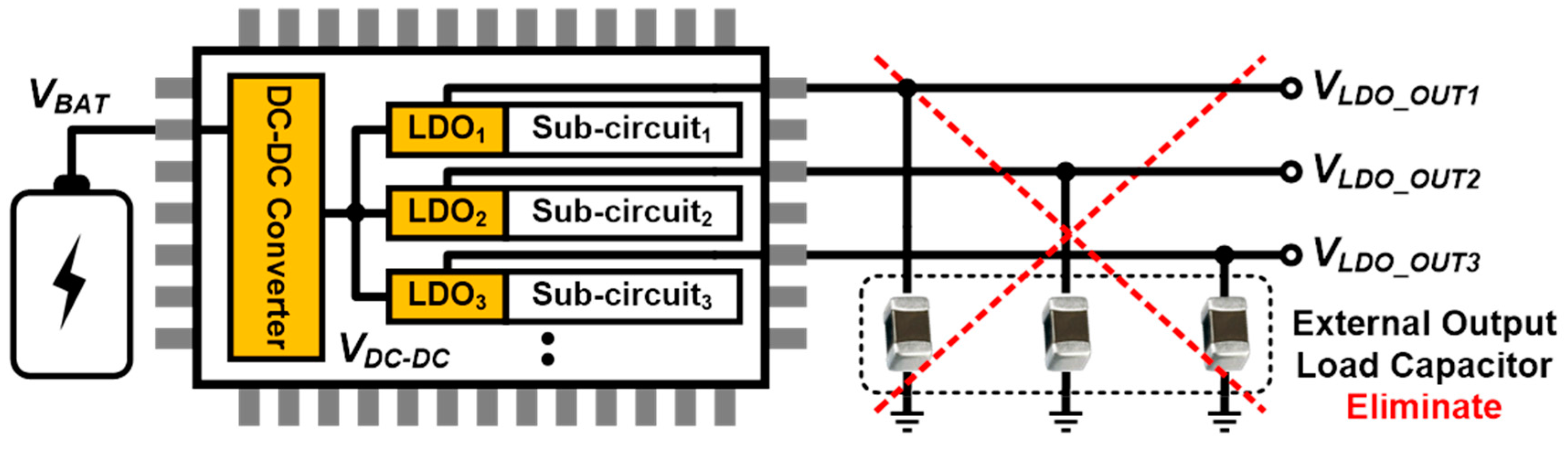
Development of miniature wireless communication chip has led to great development of mobile devices and internet of things (IoT) devices. These devices receive power from the limited battery. Various voltages which are optimized power and performance for each sub-circuit are required from a battery. Therefore, a power management integrated circuit (PMIC) for efficiently managing battery power and supplying various voltages has been attracting great interest [1,2,3,4,5,6,7,8,9,10]. As shown in Figure 1, the PMIC which is combined a switching DC-DC converter and low dropout linear regulator (LDO) is commonly used for converting DC voltage [6,7,8,9,10,11]. A high efficiency switching converter is used to convert DC voltage, and LDOs are used to remove the switching ripple and provide stable power to sub-circuits. Many systems-on-chips (SoC) require various supply voltages to separate power planes and reduce crosstalk arising from each sub-system, so that the required number of LDO is increasing. Traditional LDO has employed a large compensation capacitor to guarantee loop stability, but these bulky compensation capacitors are not feasible to be integrated on the chip. Thus, output capacitor-less LDO (OCL-LDO) [12,13,14,15,16] that can stabilize the feedback loop without external capacitors has attracted great attention for on-chip applications. The OCL-LDO can reduce the number of off-chip components and I/O pads, thus making the system more cost-effective.
The main design issues of the OCL-LDO are to increase power conversion efficiency, minimize dropout voltage, and reduce quiescent current without decreasing transient performance. For a heavy load current, a large pass transistor seems to be suitable for power efficiency by reducing dropout voltage. However, the parasitic capacitor of a large pass transistor can degrade the phase margin significantly. Low quiescent current increases the output resistance of the LDO under light load conditions, and it moves the output pole to be lower than the unity-gain-frequency (UGF), degrading the phase margin and causing instability as a result. Increasing power conversion efficiency and phase margin are a difficult design challenge while maintaining the transient performance [12,13,14,15,16].
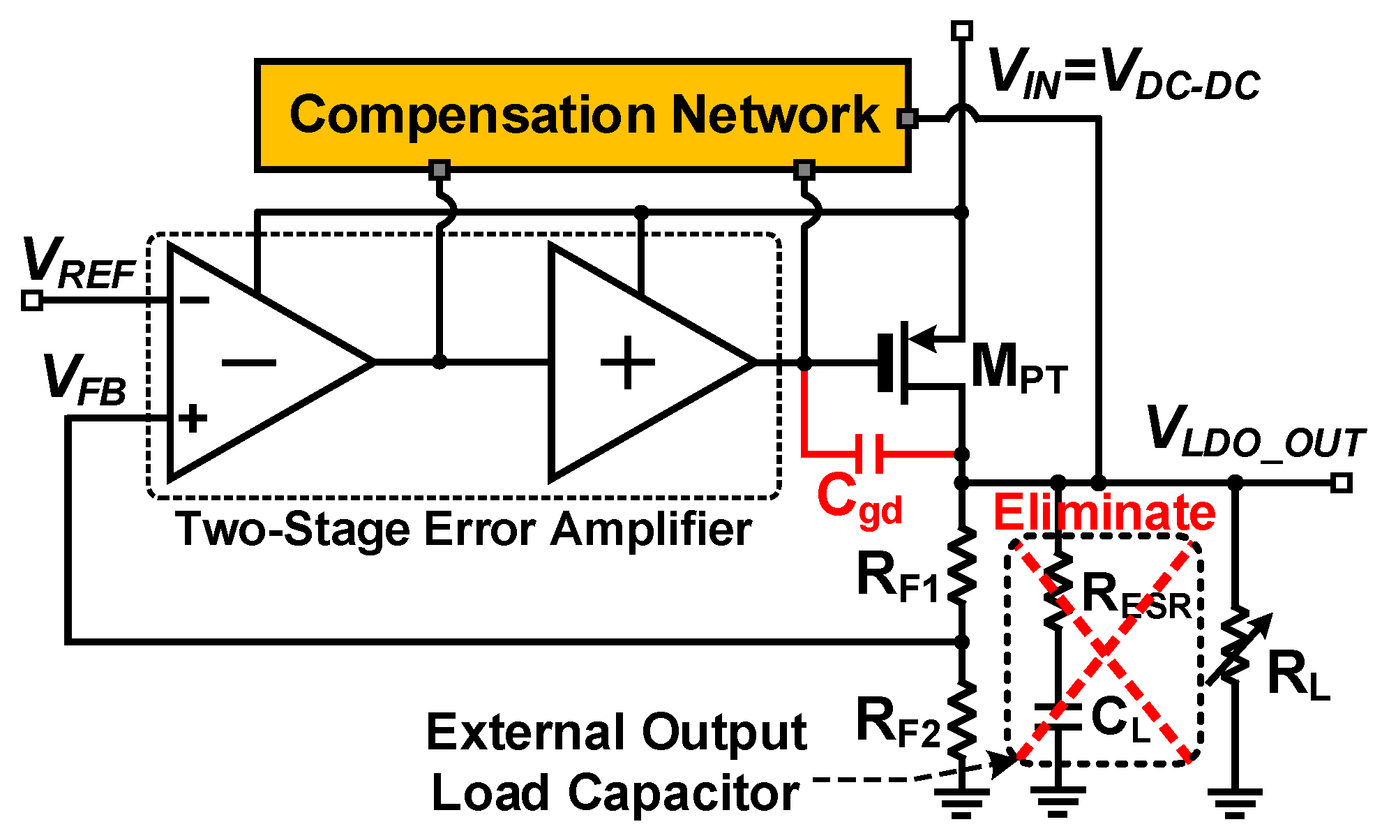
The block diagram of the OCL-LDO regulator is shown in Figure 2. The OCL-LDO typically consists of a feedback resistor ladder (RF1, RF2), an error amplifier, a power transistor (MPT), and a compensation network. The output voltage of the LDO, VLDO_OUT, is determined by the resistance ratio of the feedback resistor ladder and the reference voltage (VREF). In order to achieve high loop gain and excellent voltage regulation performance, usually a two-stage error amplifier is adopted. This amplifier compares VREF with the feedback voltage (VFB) from the output and amplifies the difference. The output signal of the error amplifier is the input signal of the power transistor (MPT) to control the output current. Since the power transistor is a common source amplifier for a small signal, the LDO loop can be regarded as a multi-stage amplifier.
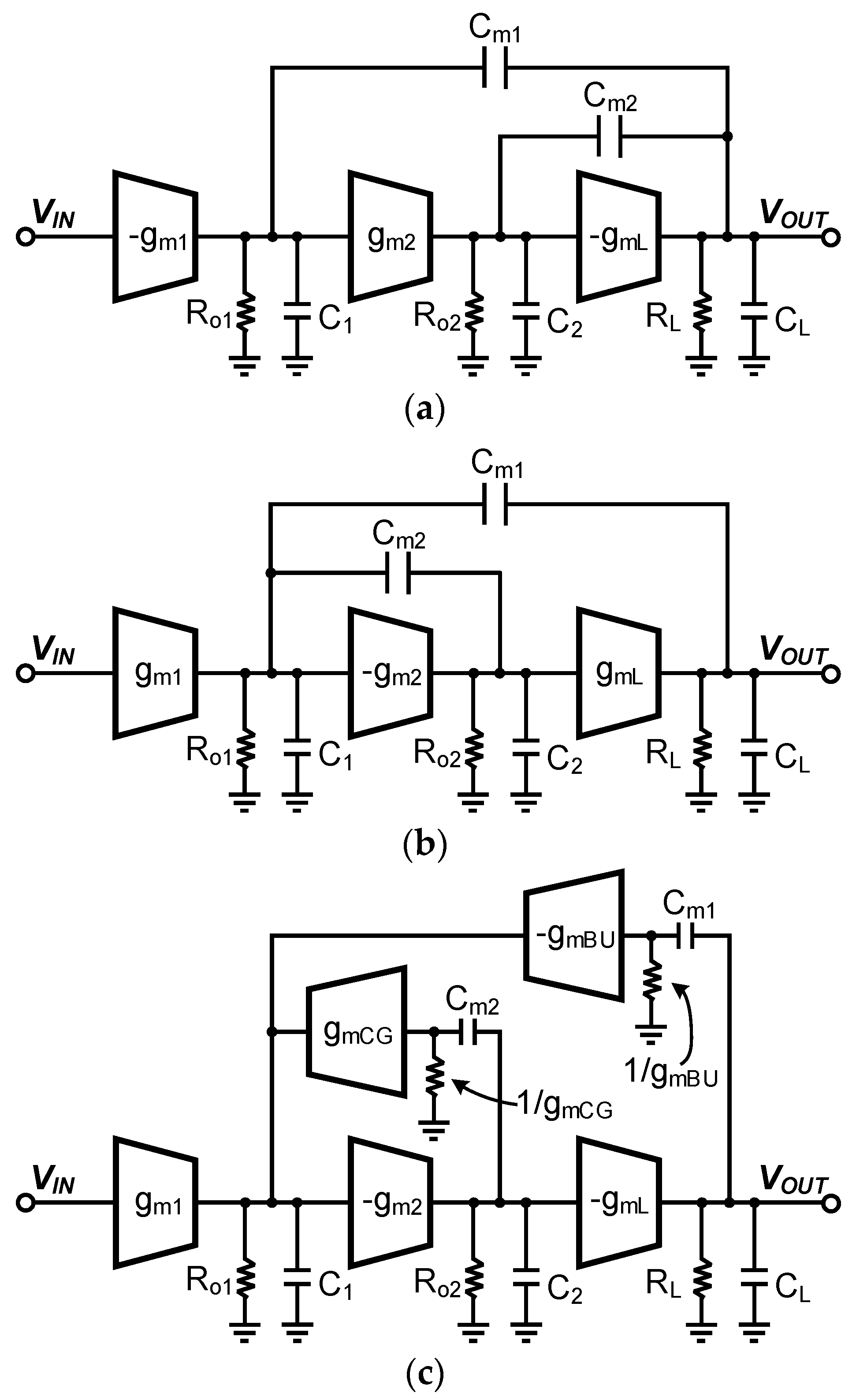
Multi-stage amplifiers which are more than two-stages should be frequency compensated and various frequency compensation methods for designing multi-stage amplifiers have been studied as shown in Figure 3 [17,18,19,20,21,22,23]. Nested Miller compensation (NMC) [17,18,19] in Figure 3a is a well-known technique which circuit parameters such as transconductance (gm) and compensation capacitors have been well-explained in [18]. Miller capacitors are connected between the output node of the final stage and the output node of each stage. These capacitors split away poles from each other. However, this technique requires large on-chip compensation capacitors to obtain sufficient phase margin. Large compensation capacitors decrease gain-bandwidth product (GBW), resulting in slow transient response or increasing current consumption. Another popular compensation method is reverse NMC (RNMC) as shown in Figure 3b. Similar to the NMC technique, a Miller capacitor is used for pole-splitting. In contrast to NMC method, Miller capacitors are connected between the output node of the first stage and the output node of each stage. This method provides higher GBW than NMC because it has a smaller capacitance to be driven at the output node [20,21]. However, this method has two right-half-plane (RHP) zeros located near the UGF, same as the NMC method [20]. The low-frequency RHP zero degrades the phase margin significantly [23]. As shown in Figure 3c, based on RNMC structure, two current buffers with Miller capacitor feedback are used to shift the RHP zeros to the left-half plane (LHP), thus increasing the phase margin [22]. However, [22] is based on a large external capacitor in the range of hundreds of nanofarads (nF) to guarantee stability and reduce output voltage overshoot, thus it requires a large on-chip compensation capacitor. This large on-chip capacitor degrades the transient performance and consumes a large area. Thus, a new compensation strategy and analysis that can be employed to the on-chip applications is required.
In this work, an active-feedback and current-reuse feedforward compensation (AFCFC) is proposed to achieve fast transient response with a low quiescent current and small on-chip capacitor. The proposed AFCFC method enables frequency compensation with small on-chip capacitor by using active feedback. RHP zero can be moved to the LHP by removing the high-frequency feedforward path formed by the Miller compensation capacitor. Also, the current reuse feedforward path shifts LHP zero to a lower frequency, thus one of the non-dominant poles can be canceled. This allows a smaller compensation capacitor to maintain a sufficient phase margin, and GBW is further improved. The proposed compensation configuration is investigated with pole-zero analysis and verified with a three-stage OCL-LDO in Section 2. The circuit implementation of the three-stage OCL-LDO using the proposed AFCFC is described in Section 3. In Section 4, measurement results are discussed and the conclusion is presented in Section 5.
2. Analysis of the Proposed AFCFC LDO
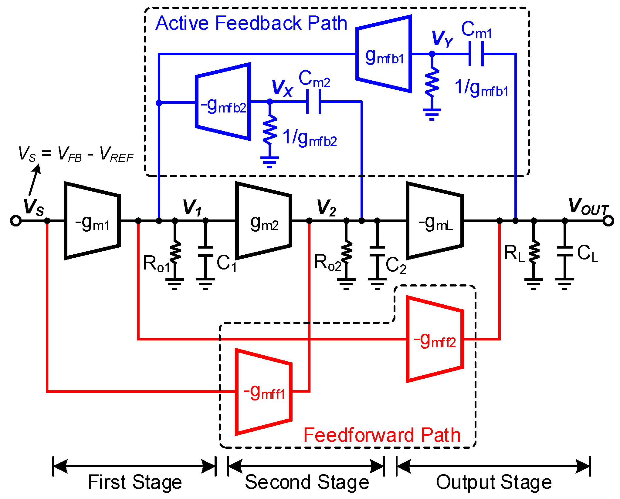
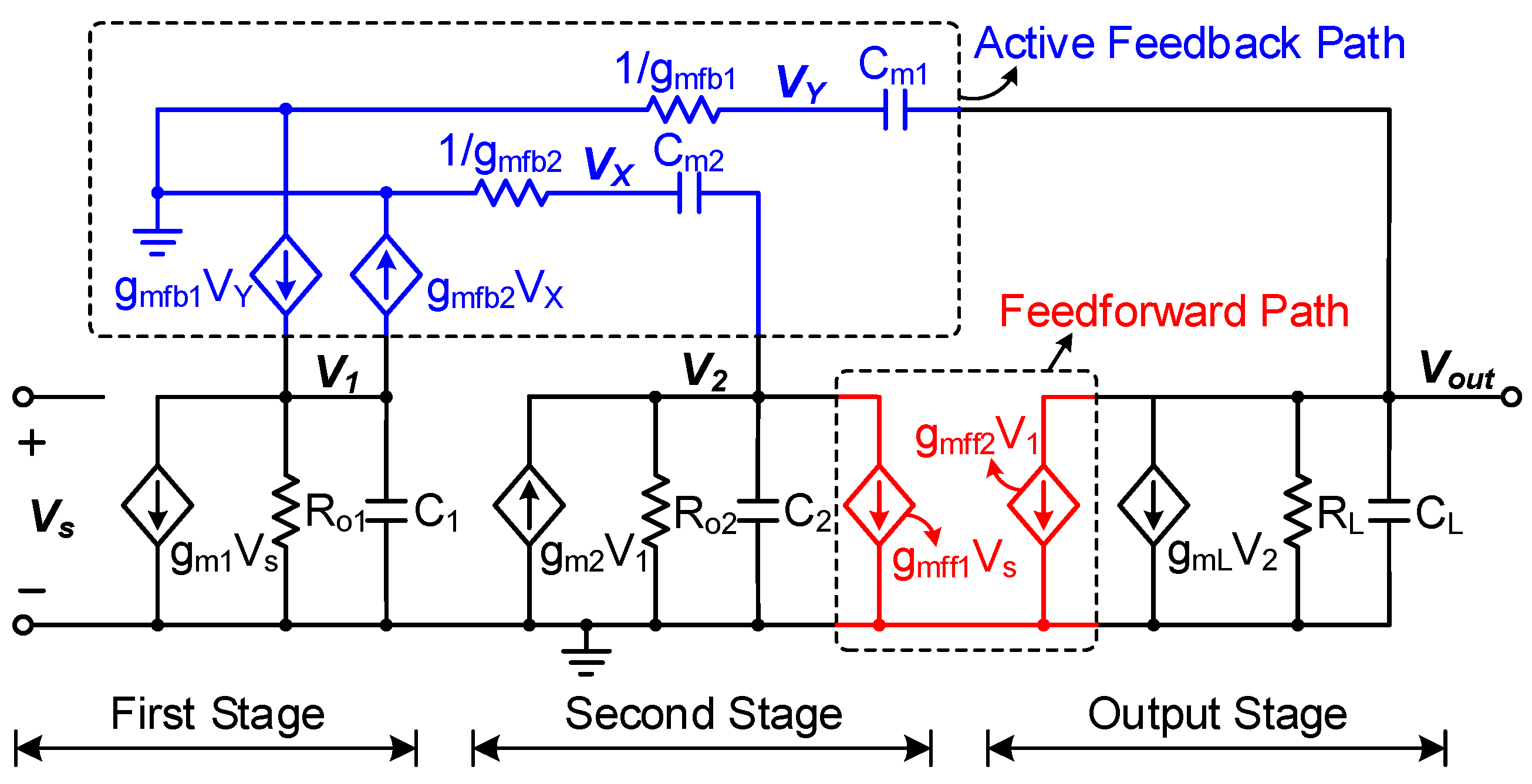
Figure 4 shows the block diagram of a three-stage amplifier employing the proposed AFCFC. The transconductances, output impedances, and lumped output capacitors of the first, second, and output stages are represented by gm1,2,L, Ro1,2,L, and C1,2,L, respectively. The active-feedback paths are depicted with transconductances of gmfb1,2 and compensation capacitors of Cm1,2. The feedforward paths are denoted by gmff1,2.
Figure 5 shows the small-signal equivalent circuit of the proposed AFCFC amplifier, and the transfer function A(s) = Vout(s)/Vin(s) can be derived in (1),
where ADC = gm1·gm2·gmL·Ro1·Ro2·RL is the DC voltage gain and p−3dB = 1/(Cm1·gm2·gm3·Ro1·Ro2·RL) is the −3 dB dominant pole frequency. To simplify the equations, two assumptions were considered. First, the gain of each stage is much larger than one. Second, two compensation capacitors and a load capacitor are much larger than the lumped output capacitors. These assumptions are represented in the equations:
The proposed system has one dominant pole, a pair of non-dominant complex poles, and two left-half-plane (LHP) zeros. Assuming that the dominant pole frequency is much lower than the complex pole and LHP zero frequencies, the gain-bandwidth product (GBW) and second non-dominant complex poles (p2,3) can be derived as:
In conventional frequency compensation methods [17,18,19,20,21,22], high frequency feedforward path is generated by Miller capacitor, thus generating RHP zeros. In the proposed AFCFC, active-feedback paths which are formed by gmfb1 and gmfb2 can effectively block the high frequency feedforward path generated by Cm1 and Cm2. Thus, the two RHP zeros are moved to LHP and the phase margin is increased.
In (1), the numerator is represented with second order terms. For a simple analysis, it assumes that the numerator of (1) has approximately two real zeros. When gm1 is equal to gmff1, two real LHP zeros can be expressed as:
When the first stage transconductance gm1 and active-feedback transconductance gmfb1,2 are equal, the two zeros can be simplified as:
It has to be noted that, since the feedforward transconductance gmff1 cancels the output stage transconductance components, the zero location is not a function of gmL but gmfb1,2, as represented in (6) and (7).
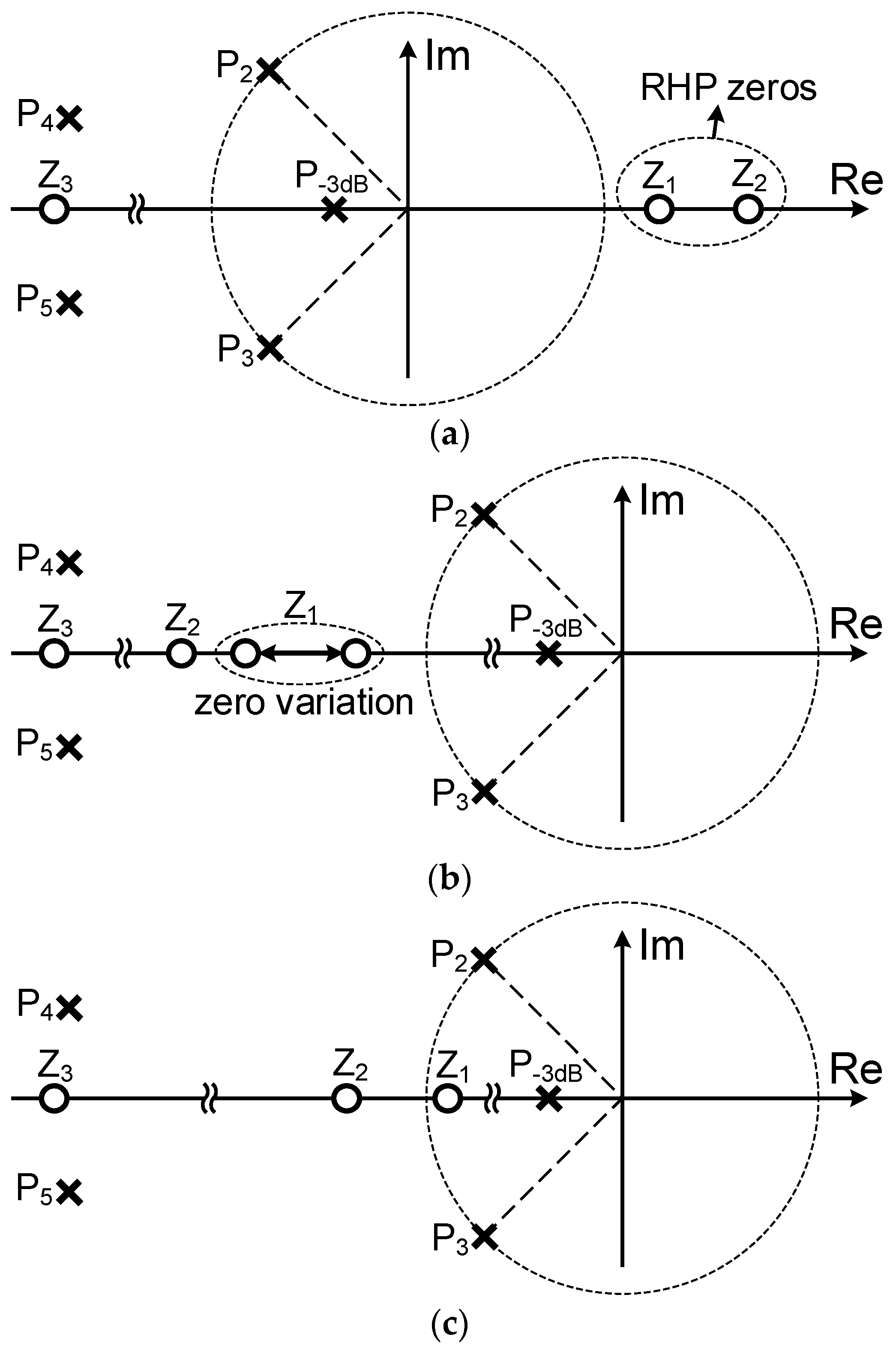
Figure 6 shows the pole-zero locations of the LDO. Figure 6a shows the pole-zero plot with two RHP zeros of NMC [17]. The RHP zeros degrade the phase margin of the LDO. The RHP zeros can be moved to the LHP using active-feedback compensation, as shown in Figure 6b. The zero variation is due to the pass transistor transconductance gmL that varies from hundreds of μA/V to tens of mA/V depending on load conditions. Although the LHP zeros do not degrade the loop stability of the LDO, active-feedback compensation without feedforward paths places the zeros at a high frequency, thus these zeros cannot remove the negative phase shift due to non-dominant complex pole p2,3. In the proposed AFCFC, the zeros are located at low frequency by adding feedforward paths, as represented in (8) and (9), due to the feedforward transconductance gmff1,2.
Typically, phase margin of 60° can be obtained by setting UGF to be half of the second non-dominant complex pole p2,3 (p2,3 > 2 × UGF). In this work, LHP zero z1 derived from (8) is located near the second complex pole p2,3, as shown in Figure 6c. Since low frequency zero z1 cancels out one of the complex pole p2,3, larger UGF can be adopted while maintaining the phase margin of 60°. In other words, a larger UGF allows a small compensation capacitor Cm1 to be used for the same gm1, so that the proposed LDO can achieve enhanced bandwidth and fast transient performance with small quiescent current. The high-frequency LHP zero z2 is located at an at-least five times higher frequency than z1, thus the z2 has little effect on the open-loop response of the LDO. The complex pole p4,5 and zero z3 depicted in Figure 6 are non-dominant components generated by inter-stage parasitic capacitor C1 and C2 in Figure 4.
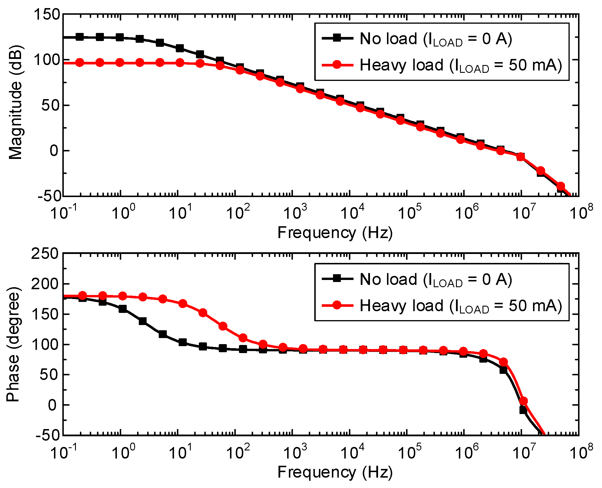
Figure 7 shows the simulated open-loop response of the proposed LDO at heavy load and light load conditions. The LDO has a high DC gain of >95 dB due to the three-stage configuration. The LDO achieves a phase margin of >62° even in the worst case, where the phase margin can be represented as:
The simulated GBW is 5.6 MHz for a light load and 4.2 MHz for a heavy load. The damping factor of p2,3 is chosen to be 0.7 or higher value to avoid gain peaking near the UGF and rapid negative phase shift that can cause phase margin degradation.
3. OCL-LDO Circuit Implementation
Figure 8 shows a schematic of the three-stage AFCFC OCL-LDO. The LDO has seven transconductance blocks. The error amplifier consists of two stages. The first stage is a folded-cascode amplifier composed of transistors M1–M12. The second stage is a cascode amplifier with a positive gain using transistors M13–M20. Both the first and the second stages have four-stacked cascade structure, so that the LDO has very large overall loop gain, as shown in Figure 7. This large loop gain increases the regulation accuracy such as load and line regulation. The output stage is composed of a pass transistor MPT, a transistor M21 for the feedforward path, and feedback resistors RF1 and RF2.
The active-feedback paths are realized with two compensation capacitor Cm1 and Cm2, and two transconductance gmfb1 and gmfb2 which are implemented by M8 and M11, respectively. gmfb1 is positive but gmfb2 is negative. Since the loops formed by the active-feedback have approximately unity gain, due to the low input impedance 1/gmfb1,2, there is no need to consider loop stability. Two feedforward transconductances, gmff1 and gmff2, are implemented with M20 and M21 respectively. Current-reuse structure is utilized with gmff1 to reduce extra quiescent current of error amplifier. Unlike gmff1, gmff2 draws extra current to reduce the output resistance and guarantee loop stability at light or no load conditions, where output resistance Rout = roPT‖ro21‖(RF1 + RF2)‖RL. The feedforward transconductance gmff2 also increases the transient performance of the LDO.
Figure 9 shows a simulated load transient with output capacitor of 100 pF. When the load current abruptly changes, the output voltage can be immediately recovered through the first stage of error amplifier and the feedforward transconductance gmff2. The load transient simulations of two cases have been performed with the same quiescent current of 60 μA. gm1,2, gmfb1,2, and gmff1 are chosen almost at the same value about 120 μA/V, and gmff2 is selected to 250 μA/V. The compensation capacitors, Cm1 and Cm2, are chosen to be 1.6 and 1 pF, respectively. The size of pass transistor MPT is 3000/0.385 μm for the maximum load current of 50 mA.
4. Implementation and Experimental Results
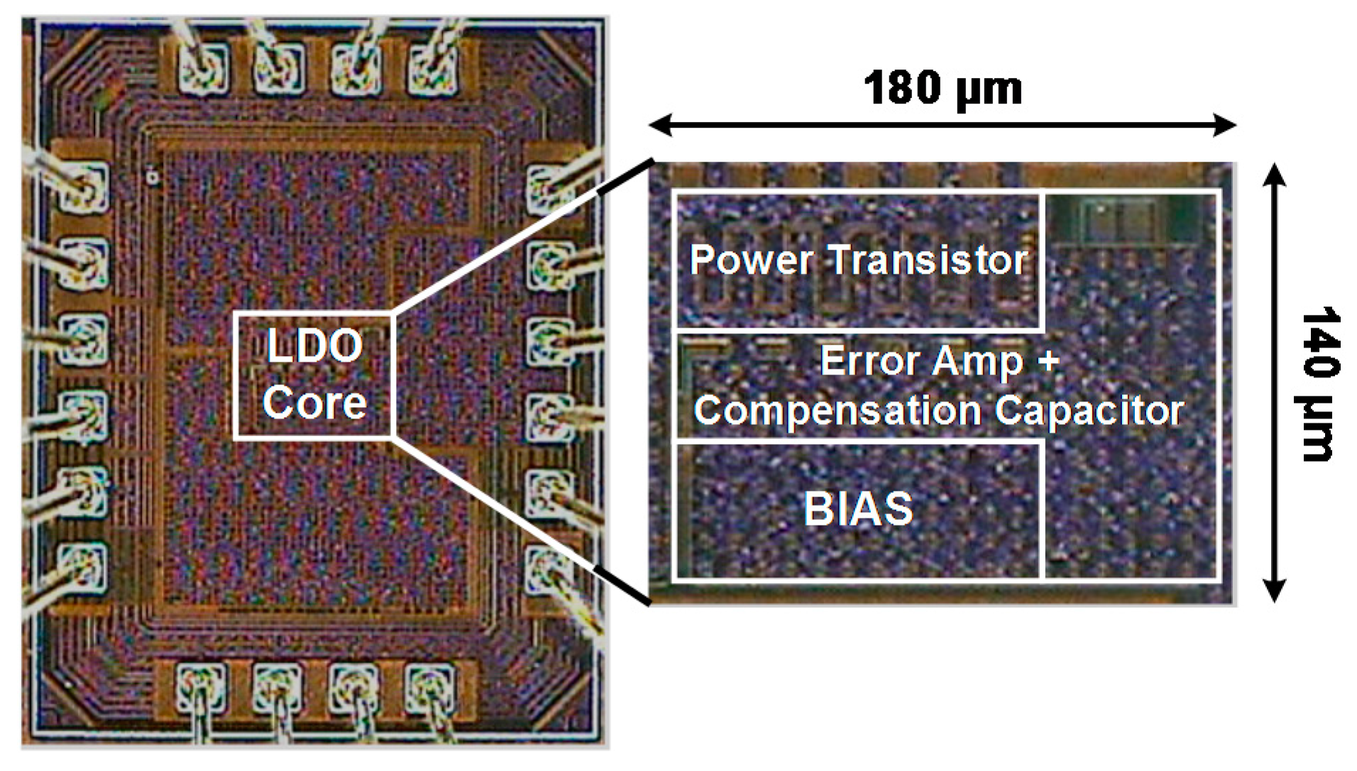
Figure 10 shows the chip photograph of the proposed AFCFC OCL-LDO, and it was fabricated using a TSMC 130 nm CMOS technology. The OCL-LDO occupies a small active area of 0.18 × 0.14 mm2 due to small compensation capacitors of the proposed AFCFC configuration. The OCL-LDO is able to supply a load current from 0 to 50 mA with the minimum dropout voltage VDO of 200 mV. The input voltage range is from 1.4 V to 2.7 V. Due to the high loop gain, the proposed OCL-LDO has good regulation accuracies such as line regulation and load regulation as shown in Table 1.
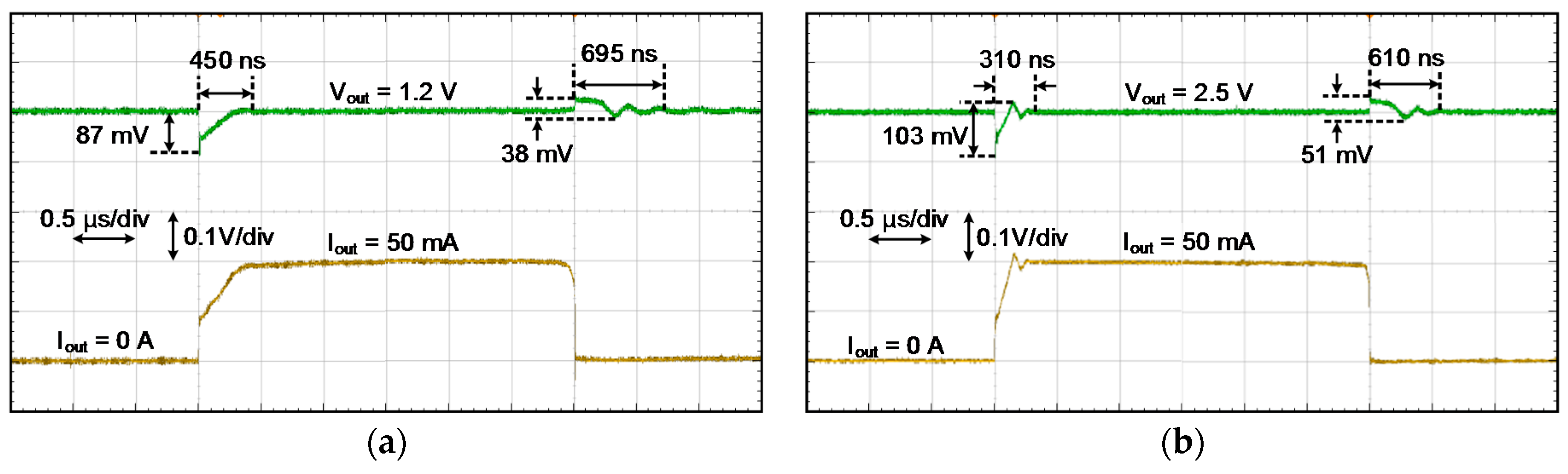
Figure 11a shows the measured load transient responses with an input supply voltage of 1.4 V and load capacitor of 100 pF. When the load current is turned-on and turned-off rapidly between 0 and 50 mA, settling times of 450 and 695 ns were obtained, respectively. The voltage overshoots of 87 mV and 38 mV were achieved for the turn-on and turn-off cases, respectively. Figure 11b shows the load transient responses with an input supply voltage of 2.7 V. The settling time is slightly enhanced to 415 and 615 ns for the turn-on and turn-off cases, respectively, due to the increased quiescent current of the error amplifier. The proposed LDO has a faster settling time compared to other works due to the proposed AFCFC.
The measured performances and comparisons of the previous-reported OCL-LDOs are summarized in Table 1. The figure-of-merit (F.o.M.) for the OCL-LDO in [12] is chosen for transient performance comparison. The F.o.M. is given as:
where CL,max, ΔVout,max, IQ, and Iout,max are the maximum load capacitor, maximum voltage overshoot, quiescent current, and maximum output current of LDO, respectively. The smaller F.o.M. shows the better performance.
5. Conclusions
An active-feedback and current-reuse feedforward compensation (AFCFC) for output capacitor-less LDO using 0.13-μm CMOS technology has been presented. The stability of the proposed LDO was analyzed using pole-zero plots, and it was confirmed by simulation results that the stability was ensured regardless of the load condition. The proposed frequency compensation allows the use of a small on-chip compensation capacitor and extends gain-bandwidth product for LDO. The fabricated LDO has high loop gain due to the three-stage configuration, thus the LDO has good regulation accuracies. The proposed LDO also has high gain-bandwidth product with low quiescent current and fast transient performance. The LDO with proposed AFCFC achieves a settling time of 450 ns with maximum load capacitor of 100 pF. The proposed LDO consumes a low quiescent current of 65.8 μA.
Acknowledgments
This work was supported by Basic Science Research Program through the National Research Foundation of Korea (NRF) funded by the Ministry of Education (NRF-2017R1D1A1B03035656) and the Chung-Ang University Graduate Research Scholarship in 2013.
Author Contributions
Eun-Taek Sung and Sangyong Park conceived, designed the circuit, performed the experiments, and wrote the manuscript as co-first authors. Donghyun Baek participated in research plan development and revised the manuscript. All authors have contributed to the manuscript.
Conflicts of Interest
The authors declare no conflict of interest.
References
- Lee, I.; Lee, Y.; Sylvester, D.; Blaauw, D. Battery voltage supervisors for miniature IoT systems. IEEE J. Solid-State Circuits 2016, 51, 2743–2756. [Google Scholar] [CrossRef]
- Yosef-Hay, Y.; Muntal, P.L.; Larsen, D.Ø.; Jørgensen, I.H.H. Capacitor-free, low drop-out linear regulator in a 180 nm CMOS for hearing aids. In Proceedings of the 2016 IEEE Nordic Circuits and Systems Conference (NORCAS), Copenhagen, Denmark, 1–2 November 2016; pp. 1–5. [Google Scholar]
- Keikhosravy, K.; Mirabbasi, S. A 0.13-μm CMOS low-power capacitor-less LDO regulator using bulk-modulation technique. IEEE Trans. Circuits Syst. I Regul. Pap. 2014, 61, 3105–3114. [Google Scholar] [CrossRef]
- Maity, A.; Patra, A. Dynamic slew enhancement technique for improving transient response in an adaptively biased low-dropout regulator. IEEE Trans. Circuits Syst. II Express Br. 2015, 62, 626–630. [Google Scholar] [CrossRef]
- Hong, S.-W.; Cho, G.-H. High-gain wide-bandwidth capacitor-less low-dropout regulator (LDO) for mobile applications utilizing frequency response of multiple feedback loops. IEEE Trans. Circuits Syst. I Regul. Pap. 2016, 63, 46–57. [Google Scholar] [CrossRef]
- Lee, Y.-J.; Qu, W.; Singh, S.; Kim, D.-Y.; Kim, K.-H.; Kim, S.-H.; Park, J.-J.; Cho, G.-H. A 200-mA digital low drop-out regulator with coarse-fine dual loop in mobile application processor. IEEE J. Solid-State Circuits 2017, 52, 64–76. [Google Scholar] [CrossRef]
- Park, Y.; Salman, E. On-chip hybrid regulator topology for portable SoCs with near-threshold operation. In Proceedings of the 2016 IEEE International Symposium on Circuits and Systems (ISCAS), Montreal, QC, Canada, 22–25 May 2016; pp. 786–789. [Google Scholar]
- Peng, S.-Y.; Liu, L.-H.; Chang, P.-K.; Wang, T.-Y.; Li, H.-Y. A power-efficient reconfigurable output-capacitor-less low-drop-out regulator for low-power analog sensing front-end. IEEE Trans. Circuits Syst. I Regul. Pap. 2017, 64, 1318–1327. [Google Scholar] [CrossRef]
- Fan, S.; Xue, Z.; Lu, H.; Song, Y.; Li, H.; Geng, L. Area-efficient on-chip DC–DC converter with multiple-output for bio-medical applications. IEEE Trans. Circuits Syst. I Regul. Pap. 2014, 61, 3298–3308. [Google Scholar] [CrossRef]
- Zheng, C.; Ma, D. Design of monolithic CMOS LDO regulator with D2 coupling and adaptive transmission control for adaptive wireless powered bio-implants. IEEE Trans. Circuits Syst. I Regul. Pap. 2011, 58, 2377–2387. [Google Scholar] [CrossRef]
- Zarate-Roldan, J.; Carreon-Bautista, S.; Costilla-Reyes, A.; Sánchez-Sinencio, E. A power management unit with 40 dB switching-noise-suppression for a thermal harvesting array. IEEE Trans. Circuits Syst. I Regul. Pap. 2015, 62, 1918–1928. [Google Scholar] [CrossRef]
- Torres, J.; El-Nozahi, M.; Amer, A.; Gopalraju, S.; Abdullah, R.; Entesari, K.; Sanchez-Sinencio, E. Low drop-out voltage regulators: Capacitor-less architecture comparison. IEEE Circuits Syst. Mag. 2014, 14, 6–26. [Google Scholar] [CrossRef]
- Park, C.; Onabajo, M.; Silva-Martinez, J. External capacitor-less low drop-out regulator with 25 dB superior power supply rejection in the 0.4–4 MHz range. IEEE J. Solid-State Circuits 2014, 49, 486–501. [Google Scholar] [CrossRef]
- Chong, S.S.; Chan, P.K. A 0.9-μA quiescent current output-capacitorless LDO regulator with adaptive power transistors in 65-nm CMOS. IEEE Trans. Circuits Syst. I Regul. Pap. 2013, 60, 1072–1081. [Google Scholar] [CrossRef]
- Yun, S.J.; Kim, J.S.; Kim, Y.S. Capless LDO regulator achieving −76 dB PSR and 96.3 fs FOM. IEEE Trans. Circuits Syst. II Express Br. 2017, 64, 1147–1151. [Google Scholar] [CrossRef]
- Hazucha, P.; Karnik, T.; Bloechel, B.A.; Parsons, C.; Finan, D.; Borkar, S. Area-efficient linear regulator with ultra-fast load regulation. IEEE J. Solid-State Circuits 2005, 40, 933–940. [Google Scholar] [CrossRef]
- Leung, K.N.; Mok, P.K. Nested Miller compensation in low-power CMOS design. IEEE Trans. Circuits Syst. II Analog Digit. Signal Process. 2001, 48, 388–394. [Google Scholar] [CrossRef]
- Leung, K.N.; Mok, P.K. Analysis of multistage amplifier-frequency compensation. IEEE Trans. Circuits Syst. I Fundam. Theory Appl. 2001, 48, 1041–1056. [Google Scholar] [CrossRef]
- Palumbo, G.; Pennisi, S. Design methodology and advances in nested-Miller compensation. IEEE Trans. Circuits Syst. I Fundam. Theory Appl. 2002, 49, 893–903. [Google Scholar] [CrossRef]
- Mita, R.; Palumbo, G.; Pennisi, S. Design guidelines for reversed nested Miller compensation in three-stage amplifiers. IEEE Trans. Circuits Syst. II Analog Digit. Signal Process. 2003, 50, 227–233. [Google Scholar] [CrossRef]
- Grasso, A.D.; Palumbo, G.; Pennisi, S. Advances in reversed nested Miller compensation. IEEE Trans. Circuits Syst. I Regul. Pap. 2007, 54, 1459–1470. [Google Scholar] [CrossRef]
- Thandri, B.K.; Silva-Martínez, J. A robust feedforward compensation scheme for multistage operational transconductance amplifiers with no Miller capacitors. IEEE J. Solid-State Circuits 2003, 38, 237–243. [Google Scholar] [CrossRef]
- Garimella, A.; Rashid, M.W.; Furth, P.M. Reverse nested Miller compensation using current buffers in a three-stage LDO. IEEE Trans. Circuits Syst. II Express Br. 2010, 57, 250–254. [Google Scholar] [CrossRef]
Figure 1.
Power management integrated circuit (PMIC) with output capacitor-less low dropout regulator (OCL-LDO) scheme.
Figure 1.
Power management integrated circuit (PMIC) with output capacitor-less low dropout regulator (OCL-LDO) scheme.

Figure 2.
Output capacitor-less LDO (OCL-LDO) regulator with the compensation network.

Figure 3.
Block diagram of conventional frequency compensation methods. (a) NMC [17,18,19]; (b) reverse NMC [20,21]; and (c) reverse NMC with current buffers [22].

Figure 4.
Three stage amplifier with the proposed AFCFC.

Figure 5.
Small-signal equivalent circuit of the proposed AFCFC.

Figure 6.
Pole-zero locations of the LDOs. (a) Conventional LDO with NMC [17]; (b) active-feedback compensation LDO without current-reuse feedforward paths; and (c) with current-reuse feedforward paths.
Figure 6.
Pole-zero locations of the LDOs. (a) Conventional LDO with NMC [17]; (b) active-feedback compensation LDO without current-reuse feedforward paths; and (c) with current-reuse feedforward paths.

Figure 7.
Simulated open-loop response of LDO at different load conditions with CL = 100 pF.

Figure 8.
Schematic of three-stage OCL-LDO regulator employing the proposed AFCFC.

Figure 9.
Simulated output voltage of load transient response with CL = 100 pF.

Figure 10.
Chip photograph.

Figure 11.
Measured load transient responses with CL = 100 pF and Iout = 0 to 50 mA. (a) Vin = 1.4 V and Vout = 1.2 V; (b) Vin = 2.7 V and Vout = 2.5 V.
Figure 11.
Measured load transient responses with CL = 100 pF and Iout = 0 to 50 mA. (a) Vin = 1.4 V and Vout = 1.2 V; (b) Vin = 2.7 V and Vout = 2.5 V.


Table 1.
Performances Comparison with Recently-Reported OCL-LDOs
| Parameter | This Work | 2014 [13] | 2013 [14] | 2017 [15] |
|---|---|---|---|---|
| Technology | 130 nm | 180 nm | 65 nm | 180 nm |
| Active Area (mm2) | 0.025 | 0.14 | 0.017 | 0.033 |
| Iout (mA) | 0–50 | 0–50 | 0–100 | 0–100 |
| VDO (mV) | 200 | 200 | 200 | 200 |
| Vout (V) | 1.2–2.5 | 1.6 | 1 | 1.6 |
| Con-chip (pF) | 2.6 | 28 | 4.5 | 12.7 |
| CL,max (pF) | 100 | 100 | 100 | 100 |
| IQ (μA) | 65.8 | 55 | 0.9–82.4 | 71–101 |
| ΔVout,max (mV) | 87.5 | 75 | 68.8 | 210 |
| Line Reg. (mV/V) | 1.23 | N/A | 4.7 | 131 |
| Load Reg. (mV/mA) | 0.048 | 0.14 | 0.3 | N/A |
| PSR (dB) | −56@10 kHz 1 | −62@10 kHz | −58@10 kHz | −76@1 MHz |
| Settling Time (μs) | <0.7 | <6 | 6 | 0.2 |
| F.o.M. | 0.00395 | 0.00456 | 0.00321 | 0.00267 |
1 Simulation results.
© 2018 by the authors. Licensee MDPI, Basel, Switzerland. This article is an open access article distributed under the terms and conditions of the Creative Commons Attribution (CC BY) license (http://creativecommons.org/licenses/by/4.0/).
Share and Cite
MDPI and ACS Style
Sung, E.-T.; Park, S.; Baek, D. A Fast-Transient Output Capacitor-Less Low-Dropout Regulator Using Active-Feedback and Current-Reuse Feedforward Compensation. Energies 2018, 11, 688. https://0-doi-org.brum.beds.ac.uk/10.3390/en11030688
AMA Style
Sung E-T, Park S, Baek D. A Fast-Transient Output Capacitor-Less Low-Dropout Regulator Using Active-Feedback and Current-Reuse Feedforward Compensation. Energies. 2018; 11(3):688. https://0-doi-org.brum.beds.ac.uk/10.3390/en11030688
Chicago/Turabian StyleSung, Eun-Taek, Sangyong Park, and Donghyun Baek. 2018. "A Fast-Transient Output Capacitor-Less Low-Dropout Regulator Using Active-Feedback and Current-Reuse Feedforward Compensation" Energies 11, no. 3: 688. https://0-doi-org.brum.beds.ac.uk/10.3390/en11030688
Note that from the first issue of 2016, this journal uses article numbers instead of page numbers. See further details here.