Research on the Inductance/Capacitance Switch Model for an LCC-HVDC Converter in an AC/DC Hybrid Grid

1
School of Electronic Information and Electrical Engineering, Shanghai Jiao Tong University, Shanghai 200240, China
2
China Electric Power Research Institute, Beijing 100192, China
*
Authors to whom correspondence should be addressed.
Energies 2018, 11(4), 692; https://0-doi-org.brum.beds.ac.uk/10.3390/en11040692
Submission received: 2 March 2018
/
Revised: 15 March 2018
/
Accepted: 16 March 2018
/
Published: 21 March 2018
(This article belongs to the Special Issue Emerging Power Electronics Technologies for Power Systems and Machine Drives)
Abstract
:In order to improve the simulation speed of the AC/DC hybrid grid, the inductance/capacitance (L/C) switch model for line-commutated converter of high-voltage direct current (LCC-HVDC) is presented in this study. The time domain modeling method is used to analyze the circuit of L/C switch model for the six-pulse system in LCC-HVDC in a switching period. A parameter setting method of L/C switch model is proposed considering the transient response, the steady state performance, switching losses and simulation error of the switch. The inductance/capacitance (L/C) switch model for LCC-HVDC has the advantage of keeping the admittance matrix unchanged regardless of the change of switching state, which improves the simulation efficiency. Finally, the validity of the parameter setting method is verified. Compared with the test results of PSCAD/EMTDC, the accuracy of the proposed LCC-HVDC simulation model is proved. The model is suitable for real-time or offline simulation of AC/DC hybrid grid.
1. Introduction
An AC and DC hybrid is becoming one of the main features of the modern power grid in China. In an AC/DC hybrid grid, the interaction between AC and DC and mutual influences between sending and receiving ends changes the system characteristics significantly. Line commutated converter HVDC (LCC-HVDC) has high level of voltage and large transmission capacity and it is the main component of AC/DC power network [1,2].
Power system simulation is an important tool for analysis of grid characteristics and fault mechanism. For the early simulation studies of LCC-HVDC, the quasi-steady-state model is adopted based on electromechanical transient simulation [3]. In the simulation of asymmetric fault and waveform distortion, the non-fundamental component is generated, and the simulation result is not accurate enough. Based on the time-varying Fourier coefficients, the dynamic phasors method is used to model LCC-HVDC [4,5,6,7]. This model can reflect the dynamic behavior of the system, but it is an average-value model. The simulation results are approximated as the “envelope” of the detailed time domain simulation results. As the large scale of power electronic devices widely used in AC/DC hybrid grid, their fast switching behavior generates a large number of transient processes [8,9,10,11,12]. The simulation methods above are difficult to meet the simulation demands of large scale AC/DC power systems. In order to ensure the secure and reliable operation of the large scale and complex AC/DC hybrid power grid, the electromagnetic transient simulation technique for AC/DC hybrid power grid is necessary.
Thyristor is the main device in the simulation of LCC-HVDC. One commonly used electromagnetic transient model of thyristor in LCC-HVDC is the two-value resistance model. The thyristor in the model is equivalent to a small or large resistance when it is turned on or off. However, the two-value resistance model needs to be interpolated and resynchronized several times during the switching period. Also, the admittance matrices need to be reconstructed at the switching time. When the multi-circuit HVDC transmission system is simulated, the computational complexity increases significantly. If an AC/DC hybrid power grid, which includes more than ten LCC-HVDC lines is simulated at the same time, the scale of the system matrix becomes very large, and this problem becomes more complicated. Although existing simulation platforms such as PACAD/EMTDC and RTDS (Real Time Digital Simulator) are capable of simulating large systems in detail, the simulation of even larger and more complex AC/DC hybrid system requires much greater amount of time and costs. The scale of simulation is limited.
For the modeling of power electronic devices, an inductive/capacitive (L/C) equivalent model was proposed in [13]. The model has the advantage of keeping the Dommel equivalent admittance matrix unchanged regardless of the change of switching state. It can significantly reduce the computational resources for matrix inverse. The technique has been applied on the RTDS platform in [14]. L/C model has been used to simulated voltage source converter (VSC) and modular multilevel converter (MMC) in [15,16,17]. Few literatures have applied L/C equivalent model to LCC-HVDC simulation.
The L/C model uses inductance to simulate the off condition of switch, uses capacitance and resistance series branch to simulate the on condition of switch. The choice of relevant parameters has great influence on simulation accuracy. Unlike the full controlled devices in voltage source converters, the LCC uses thyristor, a half controlled device that can only control the conduction, but not the shutoff. It relies on the power grid to provide commutation voltage. Therefore, a new parameter setting method is needed.
The inductance/capacitance (L/C) switch model for LCC-HVDC converter is presented in this paper. In Section 2, the circuit of L/C switch model for the six-pulse system in LCC-HVDC is analyzed using the time domain modeling method. Based on the analysis results, the transient response, the steady state performance, switching losses and simulation error of the switch is studied and calculated. In Section 3, a parameter setting method is proposed to reduce the difference between the ideal switch and L/C equivalent switch. In Section 4, two examples are built, five cases under steady and transient state are presented to verify the validity of the parameter setting method and the accuracy of proposed LCC-HVDC simulation model.
2. Modeling and Analysis of LCC-HVDC Based on L/C Switch Model
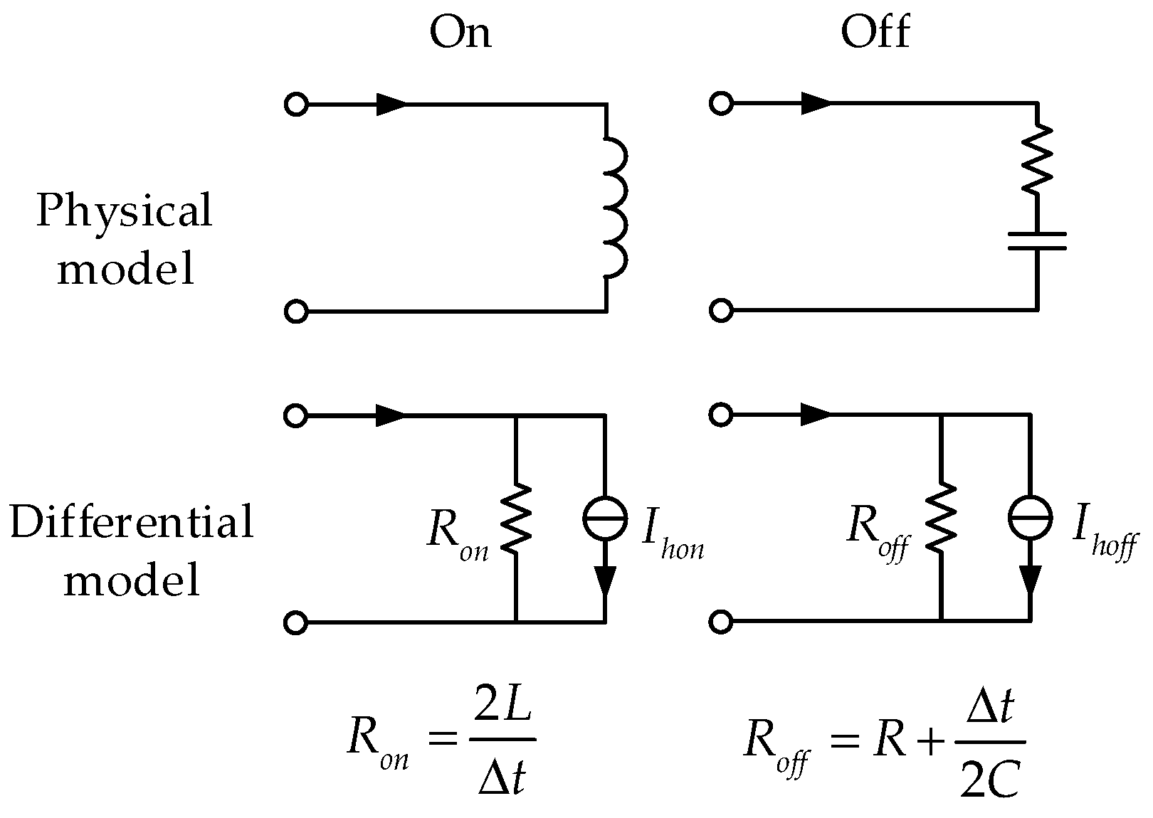
The L/C equivalent switch model was firstly proposed by the University of Sydney’s Hui and Christopoulos [13], based on the parasitic capacitance and inductance of the power electronic switching devices. Reference [18,19] made some improvements: the damping resistance R is connected in series to the capacitor branch, which accelerates the decay rate of the shock. The commonly used L/C equivalent switch model uses this structure. Taking the trapezoid method as an example, the Dommel difference model of the L/C equivalent switch is shown in Figure 1.
To guarantee the equivalent admittance unchanged in the differential model, the R, L and C parameters need satisfy Ron = Roff. The difference of the switching states is the calculation method of the historical current source. So it is not necessary to regenerate the admittance matrix with the change of the switching state in simulation.
There are some advantages using the L/C equivalent switch model in LCC-HVDC simulation. Firstly, topology of LCC-HVDC includes transformers, smoothing reactor and other inductive devices. Inductance is used to simulate the on state of thyristor, which is equivalent to a small inductance in series. Secondly, in order to reduce the high voltage of thyristor caused by voltage oscillation when thyristor turns off and to inhibit the changing rate of voltage, RC (resistance and capacitance) damping circuit is parallel to the thyristor. RC series branch is used to simulate the off state of thyristor, which is equivalent to the thyristor are ideal switch, and the grid voltage is directly applied to the damping circuit. Thirdly, LCC-HVDC has a relatively low switching frequency. Because of energy storage components used in equivalent switch model, a certain amount of energy is stored. When the switch state changes, unnecessary energy loss is generated. Compared to VSC, the L/C equivalent switch model for LCC-HVDC simulation produces less switching losses.
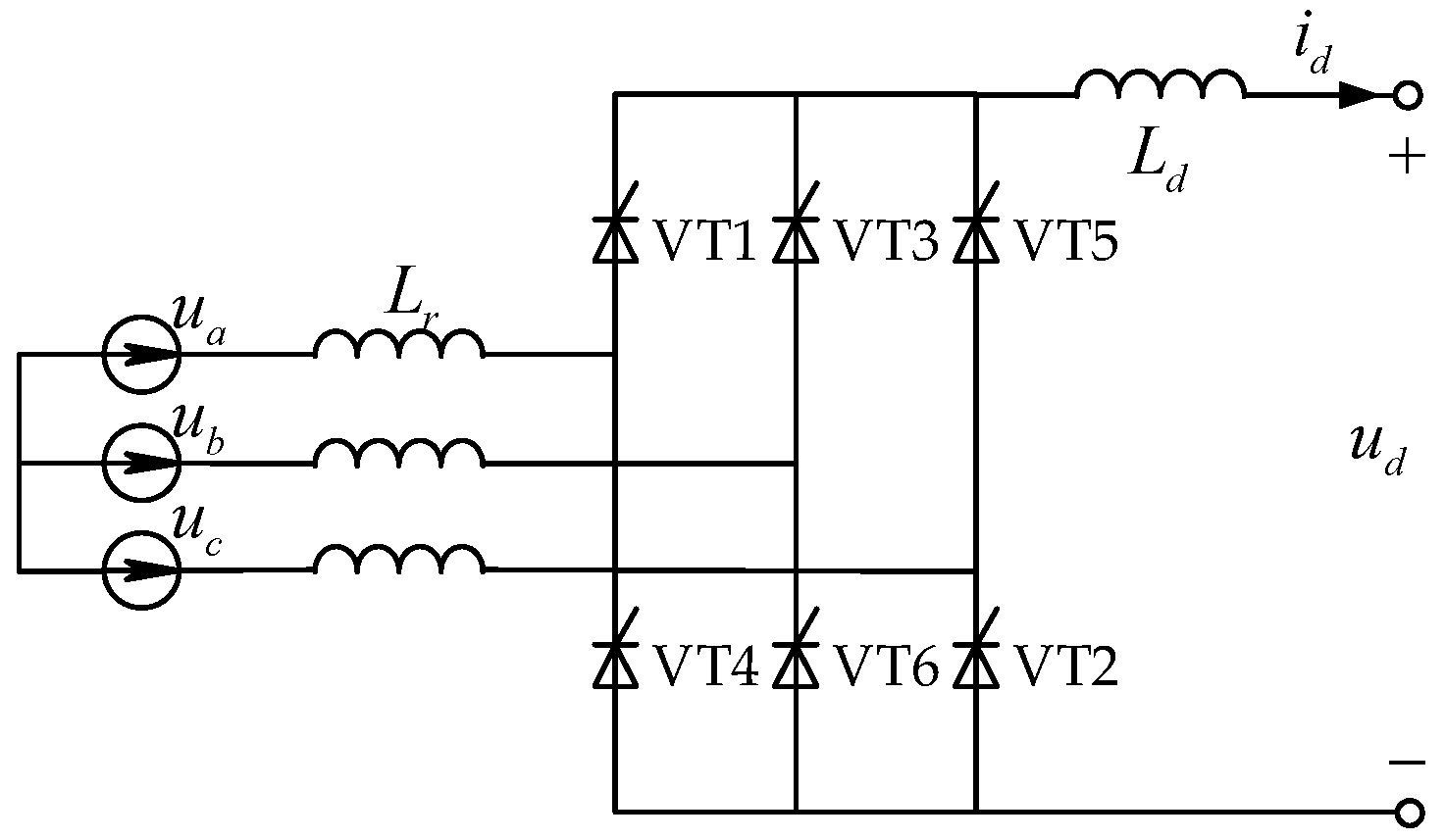
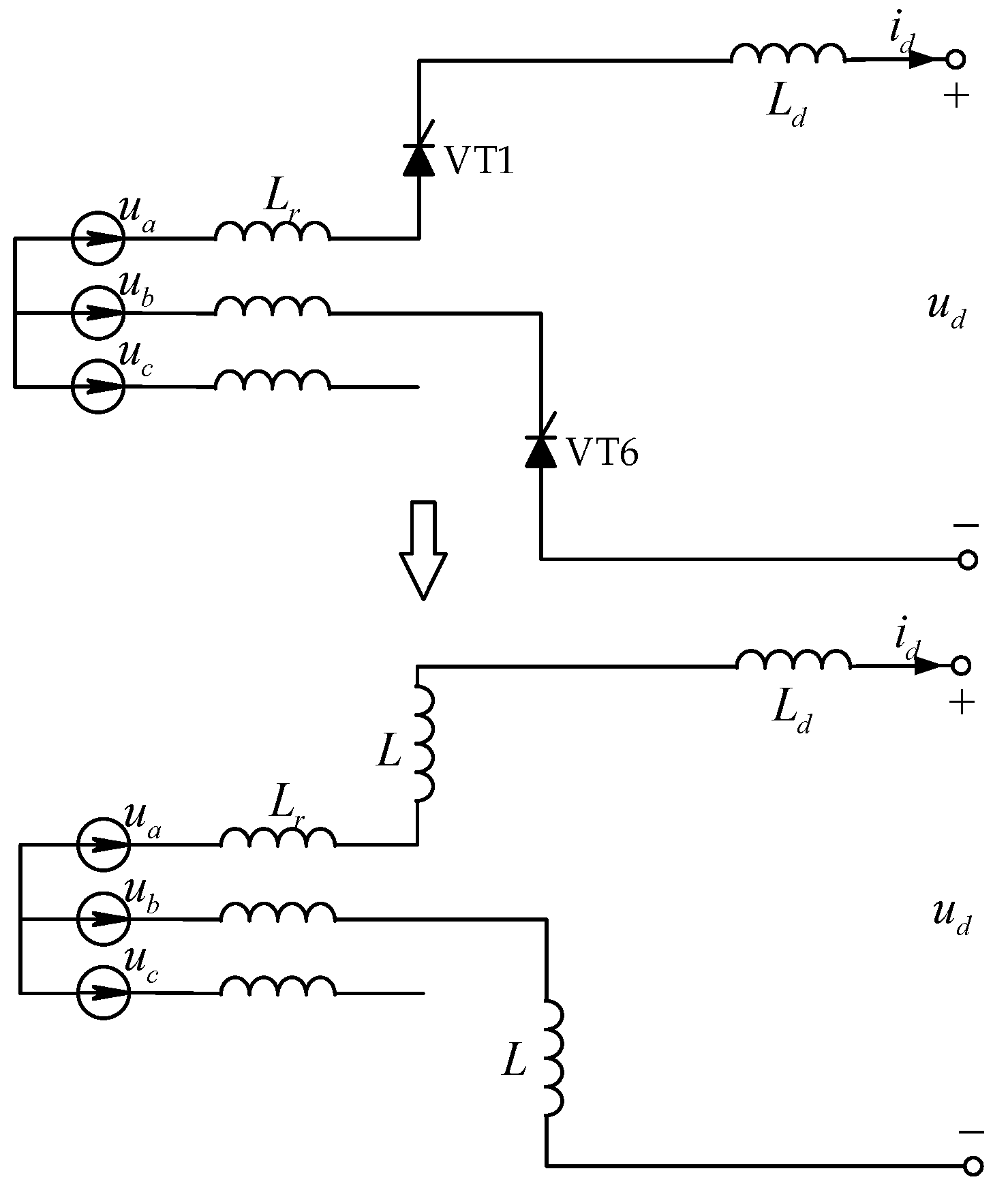
The rectifier and the inverter used in the HVDC are composed of six pulse rectifiers or inverters. The six-pulse rectifier system with L/C equivalent switch will be analyzed in the following part during one switching cycle. A simplified circuit of a six pulse rectifier system working principle is shown in Figure 2.
, and are three-phase voltage of AC bus at rectifier side. is the equivalent inductance of transformer. is smoothing reactor. Assuming that the three-phase voltage is a power-frequency sine wave, VT1 to VT6 are triggered alternately in equal intervals. Three-phase voltage in AC side is balanced. Instantaneous phase voltage can be expressed as:
is effective value of the phase voltage. VT1 has three states: conduction, off, commutation. It can be considered that the thyristor has been turned on in the commutation state.
2.1. Analysis of VT1 Voltage and Current State
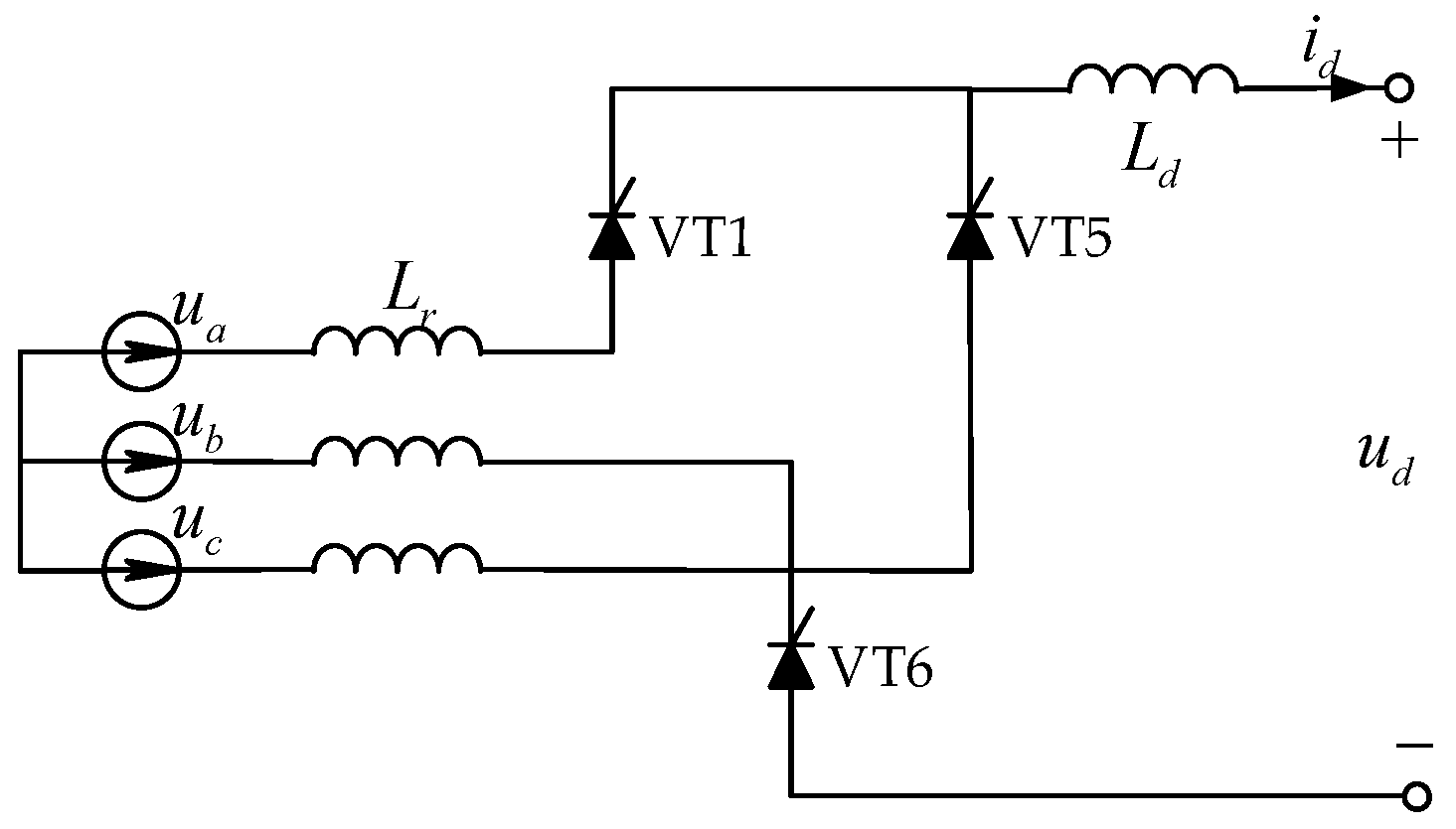
When converter valves 5, 6, 1 are turned on, the valve 1 is in conduction commutation state. The equivalent circuit is shown in Figure 3.
L/C equivalent switch uses inductance branch L to simulate the on state of switch. The equivalent circuit is shown in Figure 4.
The circuit equation can be expressed as:
can be seen as a direct current, and we can get:
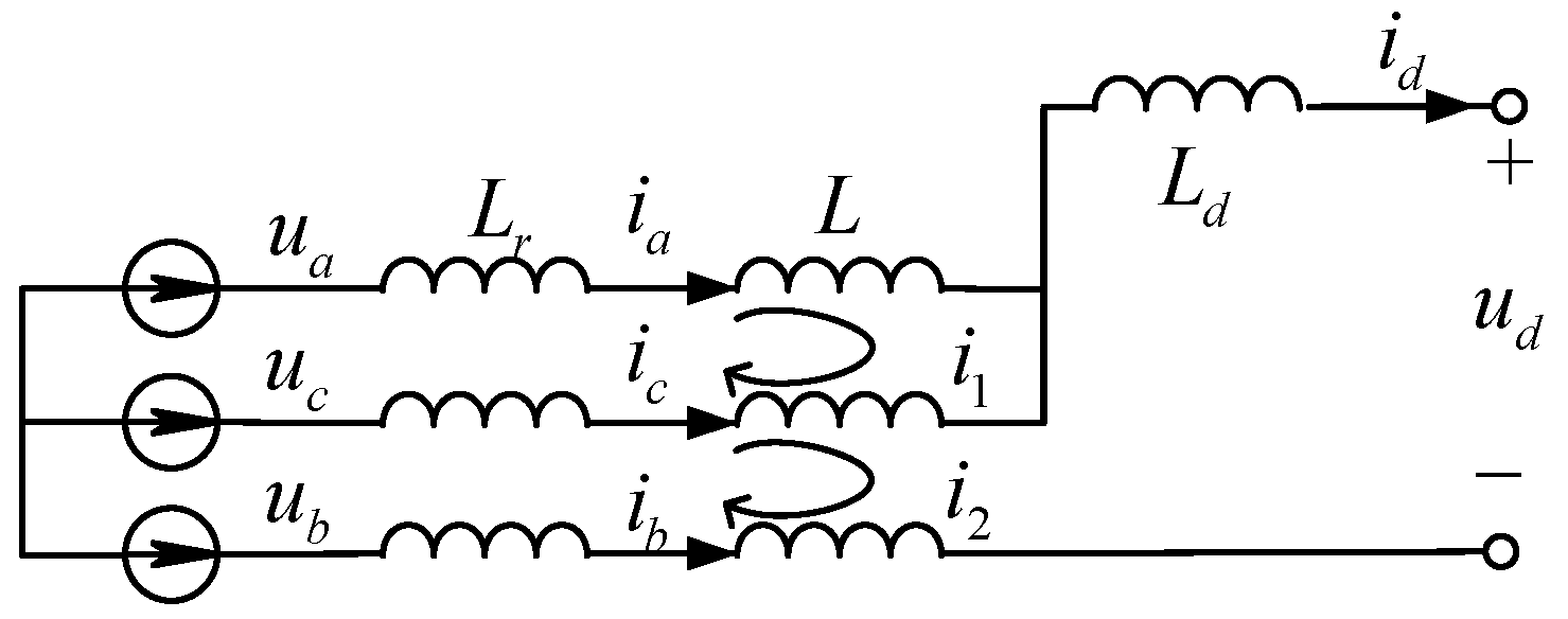
After commutation process is complete, VT1 and VT6 are in on state. The equivalent circuit is shown in Figure 5.
The circuit equation can be expressed as:
can be seen as a direct current, and we can get:
Similarly, when VT1 is in commutation or conduction condition, the DC output voltage can be listed in Table 1.
Where Thyristor firing angle; DC output current; Commutation angle, which can be calculated from the following formula:
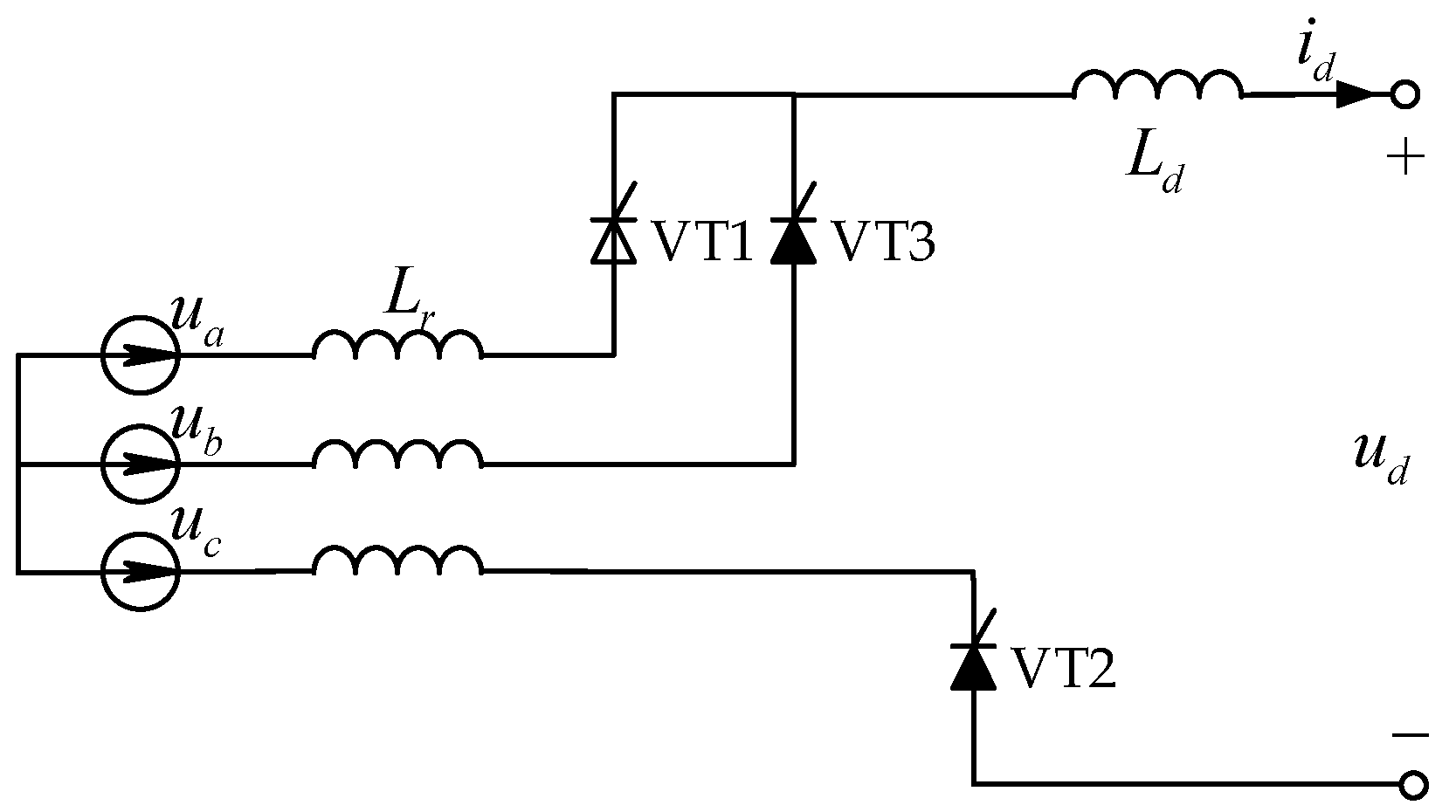
After commutation process is complete, VT1 is in off state, and VT2, VT3 are turned on. The equivalent circuit is shown in Figure 6.
The voltage of VT1:
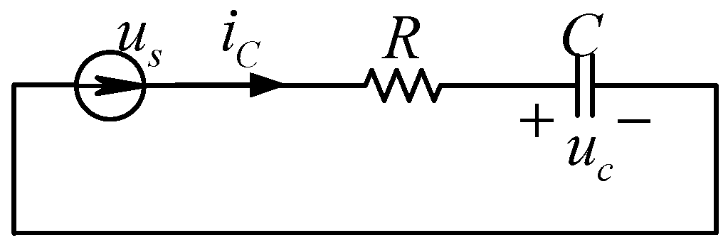
L/C equivalent switch uses RC series branch to simulate the off state of switch. The equivalent circuit of VT1 is shown in Figure 7.
Similarly, when VT1 is turned off, in a switching cycle can be listed in Table 2.
2.2. Transient Response of the Switch
When the switching state changes from on to off, the voltage of switch changes from close to zero to the line voltage in a short time, so the changing rate of voltage is very large. A capacitor is used to simulate the off state of switch, which may result in a large transient current. It is similar when the switching state changes from off to on. The transient characteristics of L/C switch model are exactly the opposite of ideal switch. If the parameter setting is not appropriate, large transient voltage and current may be produced, resulting in a large simulation error. VT1 will be taken as an example in the following part.
2.2.1. Switch Closure Process
When the phase angle of A: , the state of VT1 changes from off to conduction commutation. The equivalent circuits are shown in Figure 3 and Figure 4, and the circuit equation is shown in Equation (2). can be seen as direct current:
Then obtain
The voltage of inductance L
So at the switching moment, the voltage of inductance L is shown in Equation (11).
It can be seen that unlike the ideal switch, the voltage of L/C equivalent switch is not zero during commutation. However, we can conclude from Equation (3) that if current is near DC, the DC output voltage will not be effected.
2.2.2. Switch off Process
When the phase angle of A: , the state of VT1 changes from conduction to off commutation. After commutation, when the phase angle of A: , VT1 enters the off state. The equivalent circuits are shown in Figure 6. Initial voltage value of capacitor is zero:
When the valve 1 is turned off, set the voltage of RC branch
where External applied voltage phase when VT1 is turned off.
At this time, . The circuit equation is as follows:
Then obtain
where
Then obtain
The leakage current is produced. It must be controlled within a reasonable range so that it will not have an impact on the DC output current.
If it happens to have , then maximum possible value of may be as follow:
where Simulation step size.
2.3. Steady State Response after Switching
The duration of the steady-state process after switching is longer than the transient process, and the steady-state response has a larger effect on the simulation results.
2.3.1. Steady State Response after Switch Closure
The rectified output voltage in one switching cycle is shown in Table 1. The average output voltage can be calculated as:
The on state of the switch is simulated by inductance, resulting in commutation inductance increases and commutation process becomes longer. DC output voltage at the time of commutation is relatively smaller than that at the time of conduction. So the average value of output voltage is reduced when the output current is constant.
2.3.2. Steady State Response after Switch off
We can see from (16) that after switching off, the peak of steady state current:
2.4. Switching Losses
Since the L/C equivalent switch model uses energy storage components: inductors and capacitors. If energy is stored in the energy storage element when the switch state changes, the energy loss is generated, which can be attributed to the switching loss.
2.4.1. Switch Changes from ON to Off
The corresponding model for the switch is converting inductance to resistor capacitor series circuit. The following formula can be used to describe the stored energy in the inductor:
The necessary condition for thyristor turns off is the current reduces below the freewheeling current. In the simulation, it is generally believed that when the current through the thyristor less than zero, the thyristor is turned off, and the model switches off. So at the switching moment, current of the inductor has fallen to zero, and the energy of the inductor can be considered to be zero. Therefore, when the switch is turned from on to off, it can be considered that there is no switching losses.
2.4.2. Switch Changes from Off to On
The corresponding model for the switch is converting resistor capacitor series circuit to inductance. The following formula can be used to describe the stored energy in the capacitor:
When the phase angle of A: , the condition of switch changes. At this time, voltage of RC series circuit: , has reached steady state. It is easy to calculate the voltage of capacitor:
Then switch state changes, and the energy stored in the capacitor is lost. From (21) and (22), we can obtain the expression of switching losses:
where The numbers of switches in one second.
3. L/C Equivalent Switch Parameter Setting
The purpose of the parameter setting is to make the L/C equivalent switch behaves similarly to the ideal switch. According to the analysis results above, the performance of the two switches are as shown in Table 3.
The main differences between the L/C equivalent switch and the ideal switch is the transient response when the switch is turned off and the steady-state response. Equation (24) is used to measure the differences.
where
- The calculation result of L/C equivalent switch numbered .
- The calculation result of ideal switch numbered .
- The reference value numbered .
The optimization steps are as follows:
(1) Find the solution set to satisfy (25)
The purpose of this step is to find the solution set that meet the precision requirements of the output voltage in the range of endurance. .
(2) Find the solution satisfying Equation (26) from the solution set obtained in step (1)
This step could help us find the minimum transient and steady state current. .
(3) Find the solution set to satisfy (27) from the solution set obtained in step (1)
On the basis of the step (2), the search scope is enlarged. .
(4) Find the solution satisfying Equation (28) from the solution set obtained in step (3)
The invariant matrix before and after the switch is actually a constraint. The constraints of several commonly used integration methods are shown in Table 4.
4. Example Validation
In order to verify the validity of the parameter setting method and the accuracy of proposed LCC-HVDC simulation model, two examples are built in the following part. Example A is a six pulse rectifier system. It can help us learn about the steady state performance of L/C model without the influence of control system. Example B is a single-bridge six-pulse HVDC simulation system. Control system is added and four cases are tested on the system. It shows the transient performance of L/C model [20,21]. All examples are built in PSCAD/EMTDC (V4.5, Manitoba HVDC Research Centre, Winnipeg, Manitoba, Canada), and simulation results of L/C model will be compared with the two-value resistance model used in PSCAD/EMTDC.
4.1. Six Pulse Rectifier System
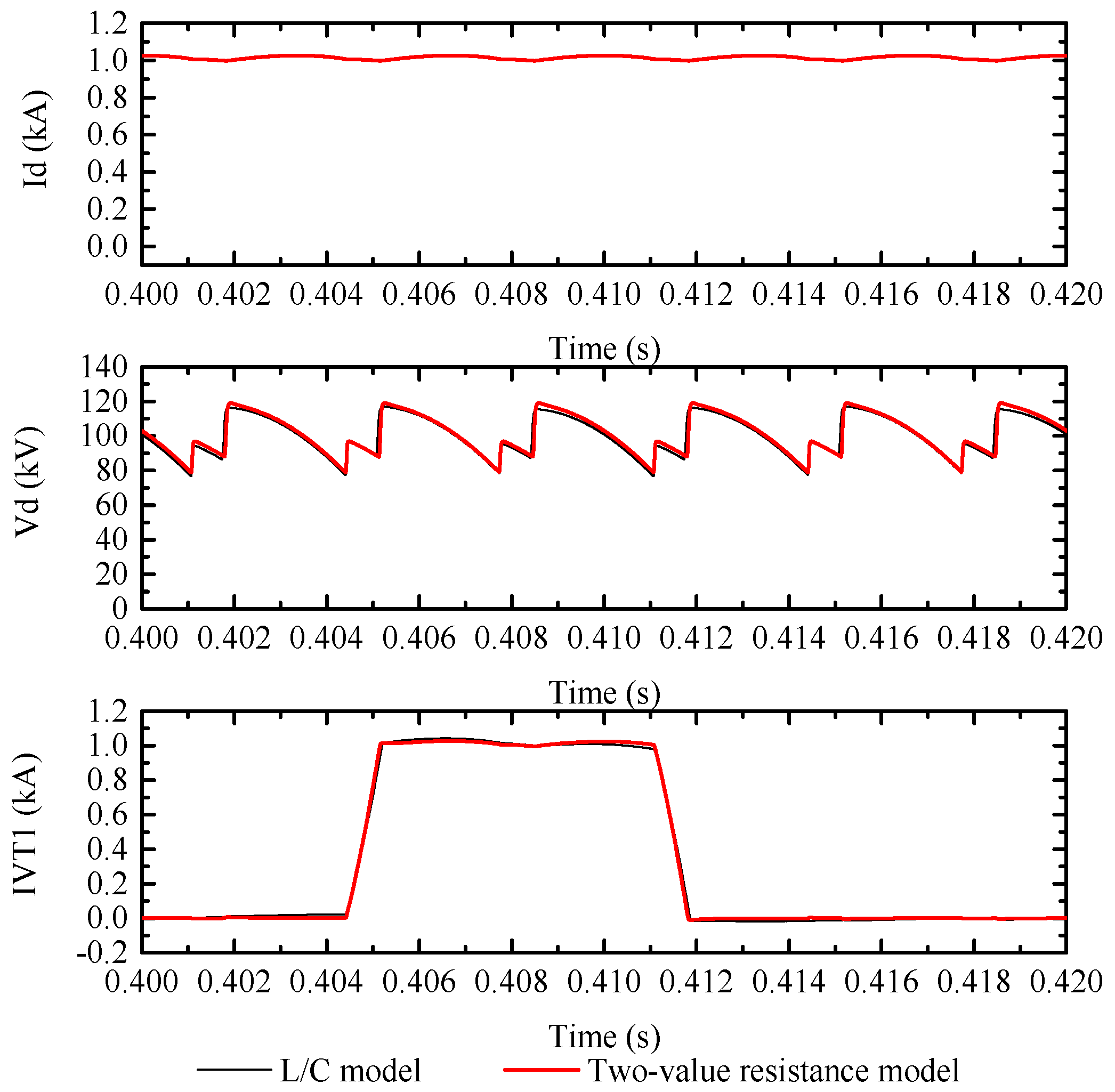
A six pulse rectifier simulation system is shown in Figure 8. System parameters are as follows: = 220 kV, = 50 Hz, = 100 Ω, = 0.6 H, = 0.023 H. Firing angle of thyristor is set as a constant: . Figure 9 shows the DC current, DC voltage, the current of VT1 respectively. The black lines represent the result of L/C model and the red lines represent the result of two-value resistance model.
The simulation results of current and DC voltage using the two models are quite close. The leakage current of L/C model is limited small enough and big transient current does not appear.
In general, the simulation results of L/C model are quite same as two-value resistance model in PSCAD/EMTDC. The proposed parameter setting method is valid.
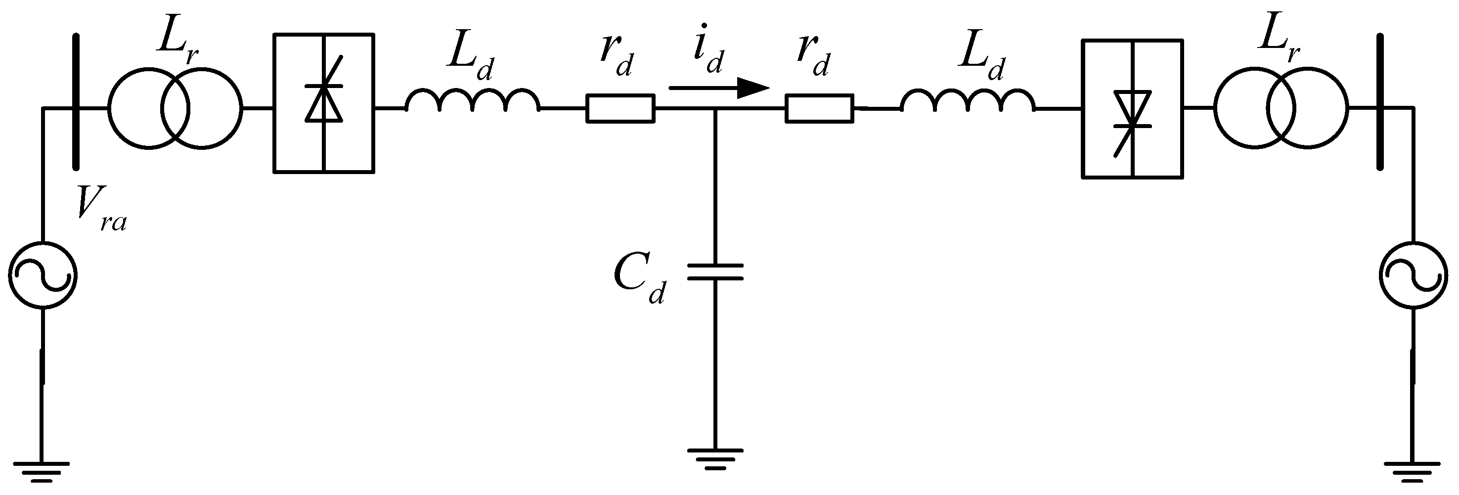
4.2. Single-Bridge Six-Pulse HVDC System
A single-bridge six-pulse HVDC simulation system is shown in Figure 10. System parameters are as follows [22]: = 220 kV, = 100 kV, = 50 Hz, = 1 Ω, = 0.6 H, = 0.023 H, = 26 μF. The rectifier control system follows its direct current order via adjusting the converter’s firing angle and the inverter control system follows its direct voltage order. The simulation step is .
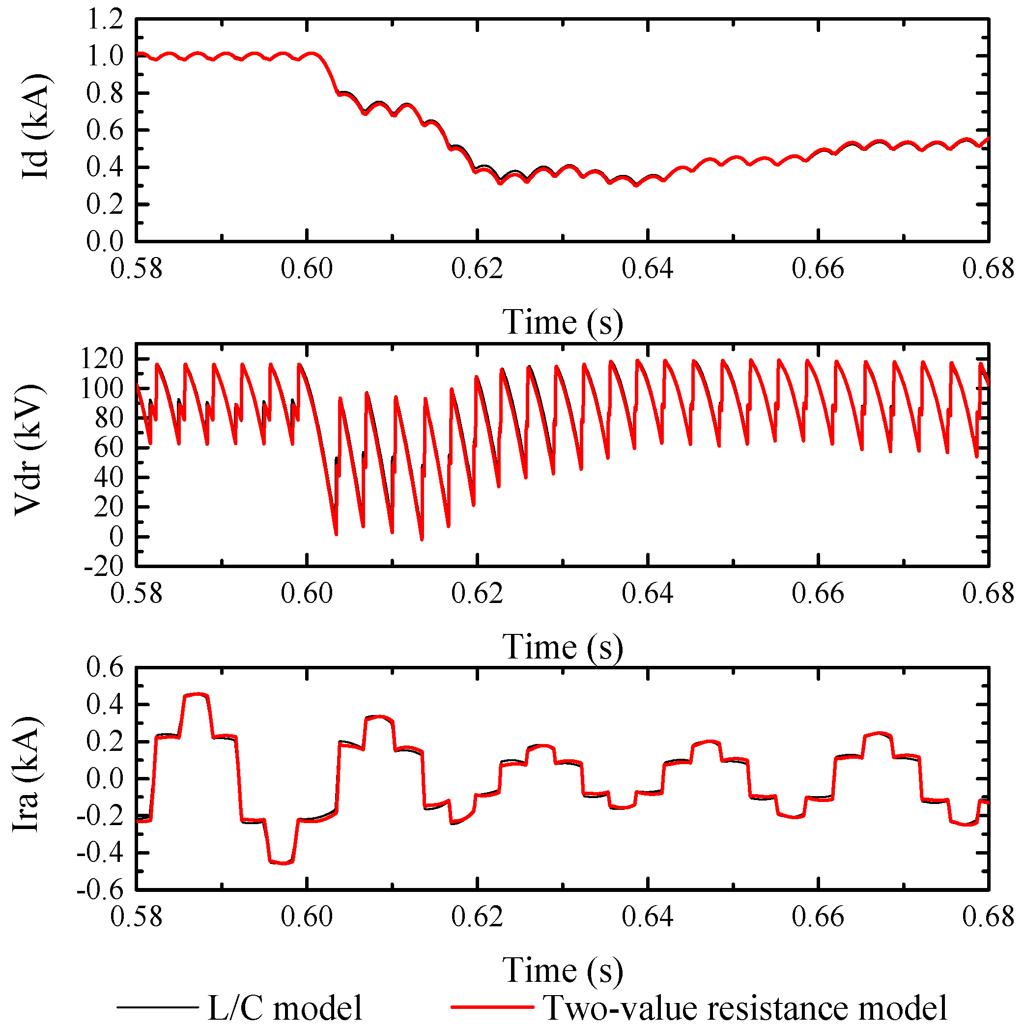
4.2.1. Step Response of the System (Case 1)
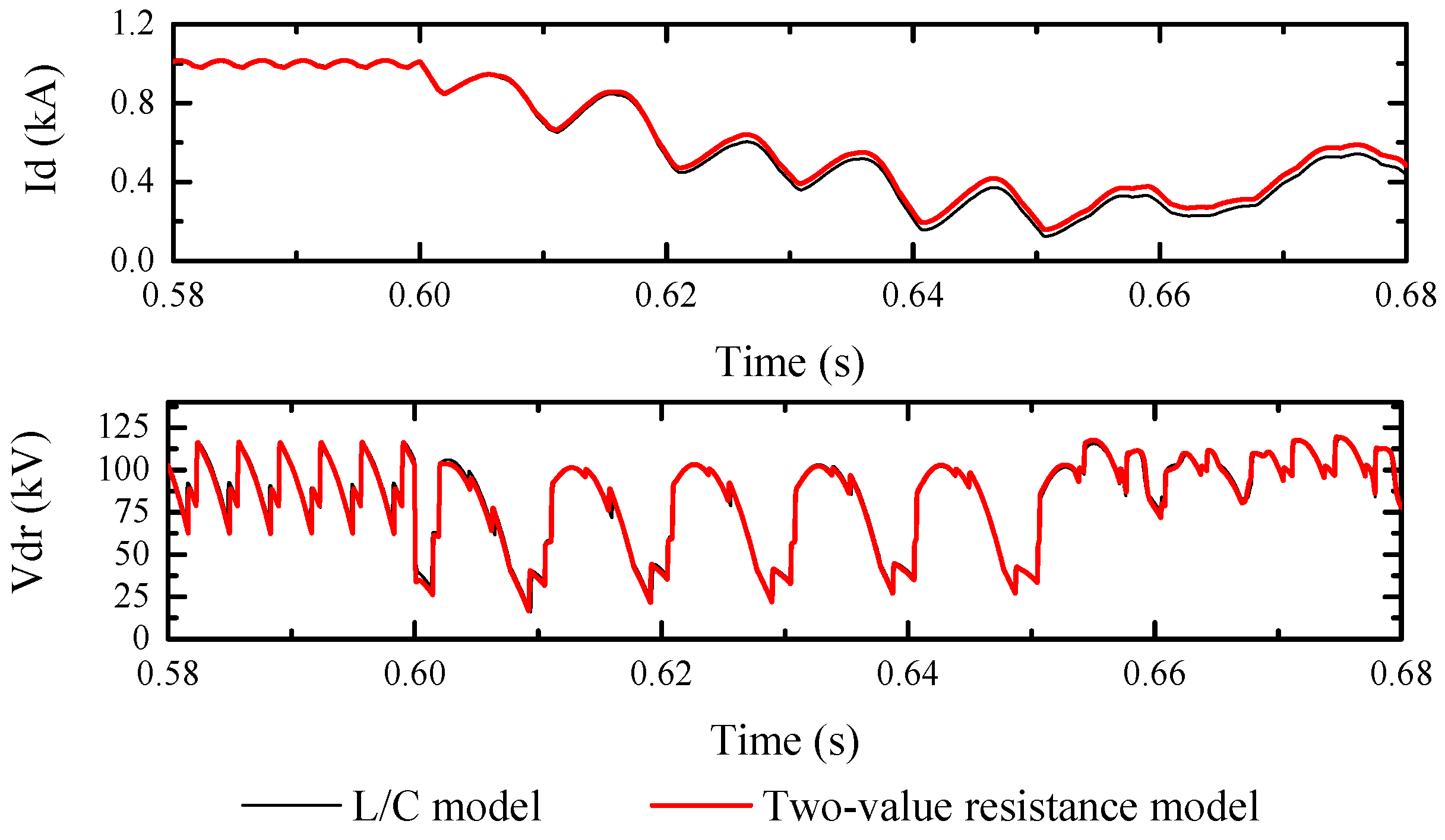
At 0.6 s, the current order is changed from 1.0 kA to 0.5 kA. Simulation results are shown in Figure 11. The red line is the result of the two-value resistance model, the black one is the result of L/C equivalent switch model. The three plots represent the curves of the rectifier DC current, the rectifier DC voltage and the AC current at rectifier side.
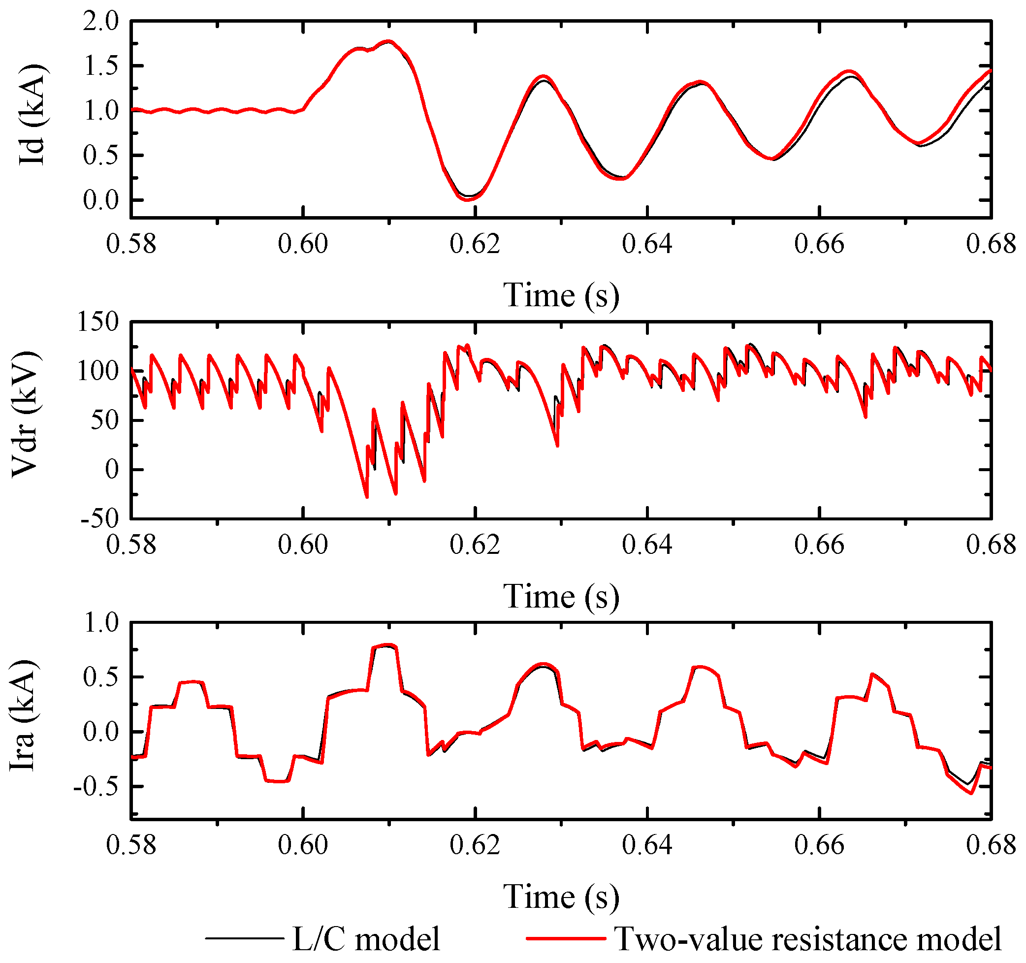
4.2.2. DC System Fault (Case 2)
At 0.6 s, a metallic ground fault occurs at the midpoint of the DC transmission line, which lasts 0.01 s. Simulation results are shown in Figure 12.
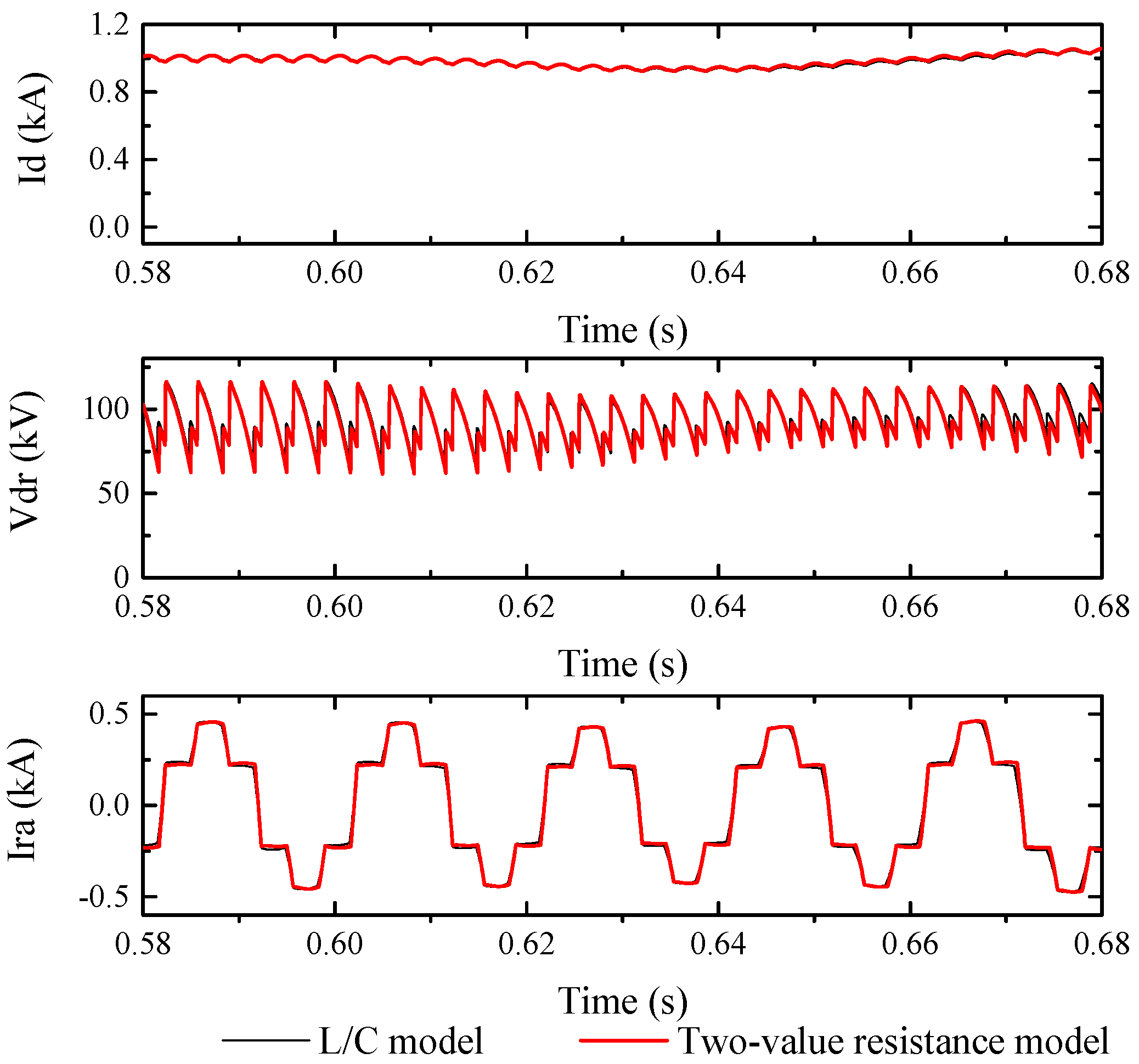
4.2.3. Voltage Drop of AC System (Case 3)
At 0.6 s, the AC bus voltage on the rectifier side is reduced by 20%, and the voltage is restored after 0.03 s. The simulation results are shown in Figure 13.
4.2.4. Commutation Failure Caused by AC System Fault (Case 4)
At 0.6 s, a metallic single-line-to-ground fault occurs at the bus of rectifier side, which lasts 0.03 s. The simulation results are shown in Figure 14.
The simulation result of L/C equivalent switch model is basically the same as PSCAD/EMTDC, which has high simulation precision.
The numbers of matrices converted during simulation and time consumed messages can be seen from the PSCAD/EMTDC output information, and they are summarized in Table 5.
It can be seen from the table that L/C model shows advantages over two-value resistance model, especially in numbers of matrices converted. As the scale of simulation is relatively small, the time consuming advantage is not significant enough.
All existing control methods of LCC-HVDC can be applied in the proposed simulation model easily. For example, the current, voltage, power and extinction angle (γ) can be controlled to generate the valve pulses. Also, this type of application performs well under all voltage levels in AC/DC hybrid grid.
5. Conclusions
In order to improve the simulation speed of the AC/DC hybrid grid, the inductance/capacitance (L/C) switch model for the LCC-HVDC converter is presented in this study.
The advantage of the L/C switch model is the system matrix can be kept constant, thus avoiding the modification of system during switch. The calculation process mainly includes matrix multiplication, which greatly reduces the computational complexity. The L/C switch model uses inductive and capacitor to simulate the switch. It mainly differs from ideal switch in three aspects. Firstly, the transient characteristics of the inductive and capacitor are exactly the opposite of ideal switch, resulting in transient error. Secondly, the use of inductance will make the process of commutation become longer, and average DC output voltage decreases. Thirdly, the use of energy storage components will result in switching losses.
To reduce the difference between the ideal switch and L/C equivalent switch, L/C model of six pulse rectifier system has been established. The time domain modeling method is used to analyze the voltage and current state in a switching period. Based on the analysis results, the transient response, the steady state performance, switching losses and simulation error of the switch is studied and calculated, then a parameter setting method is proposed.
Simulations have been performed for six pulse rectifier and single-bridge six-pulse HVDC system under normal operation, step response, DC system fault and AC system fault to test the proposed model. Test results show that the parameter setting method is valid and the proposed model is accurate and fast in simulation.
The proposed model can be used for real-time or offline simulation of the AC/DC hybrid grid.
Acknowledgments
This work was partially supported by National Key Research and Development Program of China (2016YFB0900601), National Natural Science Foundation of China (51407115, 51377104) and Shanghai Rising-Star Program (18QA1402100).
Author Contributions
Xiaodong Zheng contributed to the conception of the study; Yangyang He wrote the manuscript and contributed to the programming work; Nengling Tai and Wentao Huang helped perform the analysis with constructive suggestions; Junxian Hou revised the manuscript. All authors read and approved the manuscript.
Conflicts of Interest
The authors declare no conflict of interest.
References
- Bahrman, M.P.; Johnson, B.K. The ABCs of HVDC transmission technologies. IEEE Power Energy Mag. 2007, 5, 32–44. [Google Scholar] [CrossRef]
- Gao, B.; Zhang, R.; Li, R.; Yu, H.; Zhao, G. Subsynchronous Torsional Interaction of Wind Farms with FSIG Wind Turbines Connected to LCC-HVDC Lines. Energies 2017, 10, 1435. [Google Scholar] [CrossRef]
- Buchholz, B.M.; Lei, X.; Retzmann, D.W. Advanced solutions for power system analysis-computer study and real-time simulation. In Proceedings of the 2000 International Conference on Power System Technology, Perth, Australia, 4–7 December 2000. [Google Scholar]
- Sebastian, H. Analysis of Electromagnetic and Electromechanical Power System Transients with Dynamic Phasors. Ph.D. Thesis, University British Columbia, Vancouver, BC, Canada, 1999. [Google Scholar]
- Daryabak, M.; Filizadeh, S.; Jatskevich, J.; Davoudi, A.; Saeedifard, M.; Sood, V.K.; Martinez, J.A.; Aliprantis, D.; Cano, J.; Mehrizi-Sani, A. Modeling of LCC-HVDC Systems Using Dynamic Phasors. IEEE Trans. Power Deliv. 2014, 29, 1989–1998. [Google Scholar] [CrossRef]
- Chiniforoosh, S.; Jatskevich, J.; Yazdani, A.; Sood, V.; Dinavahi, V.; Martinez, J.A.; Ramirez, A. Definitions and Applications of Dynamic Average Models for Analysis of Power Systems. IEEE Trans. Power Deliv. 2010, 25, 2655–2669. [Google Scholar] [CrossRef]
- Shujun, Y.; Mingran, B.; Ya’nan, H.; Minxiao, H.; Junxian, H.; Lei, W. Modeling for VSC-HVDC electromechanical transient based on dynamic phasor method. In Proceedings of the 2013 Renewable Power Generation Conference, Beijing, China, 9–11 September 2013. [Google Scholar]
- Mudunkotuwa, K.; Filizadeh, S.; Annakkage, U. Development of a hybrid simulator by interfacing dynamic phasors with electromagnetic transient simulation. IET Gener. Transm. Distrib. 2017, 11, 2991–3001. [Google Scholar] [CrossRef]
- Chen, X.; Gole, A.M.; Han, M. Analysis of Mixed Inverter/Rectifier Multi-Infeed HVDC Systems. IEEE Trans. Power Deliv. 2012, 27, 1565–1573. [Google Scholar] [CrossRef]
- Chen, Z.; Chen, H.; Zhuang, M.; Bu, S. Model, Characterization, and Analysis of Steady-State Security Region in AC/DC Power System with a Large Amount of Renewable Energy. Energies 2017, 10, 1181. [Google Scholar] [CrossRef]
- Andrea, B.; Antonello, M.; Roger, A.D. Latency-Based Approach to the Simulation of Large Power Electronics Systems. IEEE Trans. Power Electron. 2014, 29, 3201–3213. [Google Scholar]
- Tarek, O.-B.; Handy, F.B.; Kamal, A.-H. A Network Tearing Technique for FPGA-Based Real-Time Simulation of Power Converters. IEEE Trans. Ind. Electron. 2015, 62, 3409–3418. [Google Scholar]
- Hui, S.Y.R.; Christopoulos, C. A discrete approach to the modeling of power electronic switching networks. IEEE Trans. Power Electron. 1990, 5, 398–403. [Google Scholar] [CrossRef]
- Qi, L.; Langston, J.; Steurer, M.; Sundaram, A. Implementation and validation of a Five-Level STATCOM Model in the RTDS small time-step environment. In Proceedings of the 2009 Power & Energy Society General Meeting, Calgary, AB, Canada, 26–30 July 2009. [Google Scholar]
- Qi, L.; Woodruff, S.; Steurer, M. Study of Power Loss of Small Time-Step VSC Model in RTDS. In Proceedings of the 2007 Power Engineering Society General Meeting, Tampa, FL, USA, 24–28 June 2007. [Google Scholar]
- Ou, K.; Maguire, T.; Warkentin, B.; Chen, Y.; Zhang, Y.; Kuffel, R.; Cai, Z.; Guan, L. Research and application of small time-step simulation for MMC VSC-HVDC in RTDS. In Proceedings of the 2014 International Conference on Power System Technology, Chengdu, China, 20–22 October 2014. [Google Scholar]
- Mu, Q.; Liang, J.; Zhou, X.; Li, Y.; Zhang, X. Improved ADC Model of Voltage-Source Converters in DC Grids. IEEE Trans. Power Electron. 2014, 29, 5738–5748. [Google Scholar] [CrossRef]
- Pejovic, P.; Maksimovic, D. A method for fast time-domain simulation of networks with switches. IEEE Trans. Power Electron. 1994, 9, 449–456. [Google Scholar] [CrossRef]
- Hui, S.Y.R.; Morrall, S. Generalised associated discrete circuit model for switching devices. IEE Proc. Sci. Meas. Technol. 1994, 141, 57–64. [Google Scholar] [CrossRef]
- Faruque, M.O.; Zhang, Y.; Dinavahi, V. Detailed modeling of CIGRE HVDC benchmark system using PSCAD/EMTDC and PSB/SIMULINK. IEEE Trans. Power Deliv. 2006, 21, 378–387. [Google Scholar] [CrossRef]
- Guo, C.; Li, C.; Zhao, C.; Ni, X.; Zha, K.; Xu, W. An Evolutional Line-Commutated Converter Integrated with Thyristor-Based Full-Bridge Module to Mitigate the Commutation Failure. IEEE Trans. Power Electron. 2017, 32, 967–976. [Google Scholar] [CrossRef]
- Wei, Z.; Liu, J.; Fang, W.; Hou, J.; Xiang, Z. Commutation Failure analysis in single- and multi-infeed HVDC systems. In Proceedings of the 2016 Power and Energy Engineering Conference, Xi’an, China, 25–28 October 2016. [Google Scholar]
Figure 1.
Differential model of L/C equivalent switch.

Figure 2.
Six pulse rectifier system working principle diagram.

Figure 3.
Equivalent circuit when VT1 is in conduction commutation state.

Figure 4.
L/C switch equivalent circuit when VT1 is in conduction commutation state.

Figure 5.
L/C switch equivalent circuit when VT1 is in conduction state.

Figure 6.
Equivalent circuit when valve 1 is turned off.

Figure 7.
L/C switch equivalent circuit when valve 1 is turned off. (: Voltage of VT1)

Figure 8.
Six pulse rectifier system.

Figure 9.
Steady state simulation results of six pulse rectifier system. (Top) DC current, (middle) DC voltage, (bottom) the current of VT1.
Figure 9.
Steady state simulation results of six pulse rectifier system. (Top) DC current, (middle) DC voltage, (bottom) the current of VT1.

Figure 10.
Single bridge six pulse HVDC system.

Figure 11.
Response of system to the current order is changed from 1.0 kA to 0.5 kA. (Top) rectifier DC current, (middle) rectifier DC voltage, (bottom) rectifier AC current (Case 1).
Figure 11.
Response of system to the current order is changed from 1.0 kA to 0.5 kA. (Top) rectifier DC current, (middle) rectifier DC voltage, (bottom) rectifier AC current (Case 1).

Figure 12.
Response of system to a metallic ground fault occurs at the midpoint of DC transmission line. (Top) rectifier DC current, (middle) rectifier DC voltage, (bottom) rectifier AC current (Case 2).
Figure 12.
Response of system to a metallic ground fault occurs at the midpoint of DC transmission line. (Top) rectifier DC current, (middle) rectifier DC voltage, (bottom) rectifier AC current (Case 2).

Figure 13.
Response of system to a 20% reduction of AC bus voltage at rectifier side. (Top) rectifier DC current, (middle) rectifier DC voltage, (bottom) rectifier AC current (Case 3).
Figure 13.
Response of system to a 20% reduction of AC bus voltage at rectifier side. (Top) rectifier DC current, (middle) rectifier DC voltage, (bottom) rectifier AC current (Case 3).

Figure 14.
Response of system to a metallic single-line-to-ground fault occurs at the bus of rectifier side. (Top) rectifier DC current, (bottom) rectifier DC voltage (Case 4).
Figure 14.
Response of system to a metallic single-line-to-ground fault occurs at the bus of rectifier side. (Top) rectifier DC current, (bottom) rectifier DC voltage (Case 4).


Table 1.
DC output voltage of L/C switch equivalent circuit.
| Phase Angle of A (Rad) | Number of Conductive Valve | |
|---|---|---|
| 5,6,1 | ||
| 6,1 | ||
| 6,1,2 | ||
| 1,2 | ||
| 1,2,3 |
Table 2.
Valve voltage of L/C switch equivalent circuit.
| Phase Angle of A (Rad) | Number of Conductive Valve | |
|---|---|---|
| 2,3 | ||
| 2,3,4 | ||
| 3,4 | ||
| 3,4,5 | ||
| 4,5 | ||
| 4,5,6 | ||
| 5,6 |
Table 3.
The difference between the L/C equivalent switch and the ideal switch.
| Number | Evaluation Options | L/C Equivalent Switch | Ideal Switch | |
|---|---|---|---|---|
| 1 | Transient response | On | ||
| 2 | Off | |||
| 3 | Steady state response | On | ||
| 4 | Off | |||
| 5 | Switching losses | On | 0 | |
| 6 | Off | 0 | 0 | |
Table 4.
The constraints of different integral methods.
| Integration Methods | Constraints |
|---|---|
| Backward Euler | |
| Implicit trapezoid | |
| Gear-3 | |
| Gear-4 |
Where Simulation step size.
Table 5.
Time consuming and numbers of matrices converted of the two model.
| Type of Model | Simulation Example | Time Consuming (s) | Numbers of Matrices Converted |
|---|---|---|---|
| L/C model | Case 1 | 6.9 | 1 |
| Case 2 | 6.7 | 3 | |
| Case 3 | 6.5 | 1 | |
| Case 4 | 6.6 | 3 | |
| Two-value resistance model | Case 1 | 7.6 | 1155 |
| Case 2 | 7.4 | 1161 | |
| Case 3 | 7.1 | 1153 | |
| Case 4 | 7.7 | 1157 |
© 2018 by the authors. Licensee MDPI, Basel, Switzerland. This article is an open access article distributed under the terms and conditions of the Creative Commons Attribution (CC BY) license (http://creativecommons.org/licenses/by/4.0/).
Share and Cite
MDPI and ACS Style
He, Y.; Zheng, X.; Tai, N.; Hou, J.; Huang, W. Research on the Inductance/Capacitance Switch Model for an LCC-HVDC Converter in an AC/DC Hybrid Grid. Energies 2018, 11, 692. https://0-doi-org.brum.beds.ac.uk/10.3390/en11040692
AMA Style
He Y, Zheng X, Tai N, Hou J, Huang W. Research on the Inductance/Capacitance Switch Model for an LCC-HVDC Converter in an AC/DC Hybrid Grid. Energies. 2018; 11(4):692. https://0-doi-org.brum.beds.ac.uk/10.3390/en11040692
Chicago/Turabian StyleHe, Yangyang, Xiaodong Zheng, Nengling Tai, Junxian Hou, and Wentao Huang. 2018. "Research on the Inductance/Capacitance Switch Model for an LCC-HVDC Converter in an AC/DC Hybrid Grid" Energies 11, no. 4: 692. https://0-doi-org.brum.beds.ac.uk/10.3390/en11040692
Note that from the first issue of 2016, this journal uses article numbers instead of page numbers. See further details here.