Two-Feeder Dynamic Voltage Restorer for Application in Custom Power Parks


1
Coordination of Electronic Engineering, Higher Technological Institute of Irapuato, Irapuato 36820, Mexico
2
Department of Electronic Engineering, DICIS, University of Guanajuato, Salamanca 36787, Mexico
*
Author to whom correspondence should be addressed.
Energies 2019, 12(17), 3248; https://0-doi-org.brum.beds.ac.uk/10.3390/en12173248
Submission received: 4 July 2019
/
Revised: 8 August 2019
/
Accepted: 9 August 2019
/
Published: 23 August 2019
Abstract
:The custom power park (CPP) is a concept that has been developed for the purpose of dealing with power quality problems. The CPP is powered by two independent feeders and consists of different types of custom power devices for compensation (dynamic voltage restorer, DVR) and reconfiguration (static transfer switch, STS). Normally, the loads are fed by the preferred feeder (PF) through the STS. When a fault occurs in the PF, the STS performs a reconfiguration of the feeders and feeds the load with an alternate feeder. In this paper, a two-input DVR based on the matrix converter is proposed to provide stable voltage to the load. Each of the DVR inputs is connected to a different feeder, and the PF powers the load. Thus, the DVR has an operational behavior like the STS when reconfiguring the energy transfer of the two feeders and injects it into the PF to guarantee a stable voltage in the load. The control algorithm in the DVR is performed in the dq reference frame to have a unit power factor in feeders and load. The modulation schemes are based on space vector modulation and modified carrier based pulse width modulation. The efficiency and multifunctionality of the proposed DVR is corroborated by simulations on the MATLAB/Simulink.
1. Introduction
Voltage distortion in an electrical network can arise by a great variety of events, from failures in transmissions lines to problems originated in equipment from end users. Commonly, these failures occur by way of voltage sags, causing interruptions in different types of industrial processes, which are reflected in considerable economic losses. Due to the increase of equipment sensitive to voltage variations and since the electrical grids must be feeder the loads without interruptions or blackouts; voltage sags have been one of the most important problems for power quality (PQ) [1,2,3].
In order to improve PQ in distribution networks, devices based on power electronics, denominated custom power devices (CPD), have been utilized [4,5,6]. These devices help to mitigate or eliminate the negative operational effects of voltage variations in sensitive equipment. Among these devices, the dynamic voltage restorer (DVR) stands out due to its operational advantages.
The DVR is an economical solution and technically the most suitable device to protect sensitive loads from sags. Normally, this device is installed where the distribution network feeds large industrial plants or large groups of sensitive loads. The operational principle of the DVR is to inject the appropriate voltage in series with the power supply through an injection transformer to restore the supply voltage under abnormal conditions. The magnitude and phase angle of the injected voltage is variable; therefore, an active or reactive power exchange is generated between the DVR and the distribution system or the load. The amount of energy that the DVR injects into the network depends on the type of disturbance to be compensated.
Due to the importance of DVRs in the suppression of disturbances in the electric network, different topologies have been developed to maintain the voltage in the load at its nominal value [7,8,9]. Generally, the DVR consists of an energy storage system, a voltage source converter, a current source inverter, a capacitor for energy storage in the DC-link, and an injection transformer. With this point of view, this paper presents a new DVR topology based on the matrix converter (MC) of two three-phase inputs. The proposed two-input DVR does not use an energy storage system, and a capacitor for energy storage in the DC-link is not necessary.
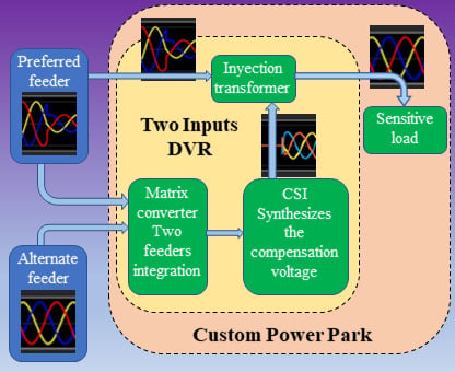
During the voltage sag, the DVR injects a voltage to restore the load voltage. When this happens, the DVR can exchange active and reactive energy with the system. If the DVR provides active power to the load, then, the DVR may need an external source to take the necessary power. Thus, in [7,8], the DVRs were classified according to the external energy storage system as follows: (a) Those that use an energy storage system (batteries, capacitors, flywheel, or super magnetic energy storage—SMES) to provide the power that must be delivered by the DVR, and (b) those that do not use energy storage systems where the DVR takes power from the failing network during voltage drop. In [9], a classification of the DVRs was made according to the requirements of the capacitor in the DC-link. In this way, the converters used in the topologies of the DVRs can be classified as AC–DC–AC converters with a DC-link and AC–AC converters without a DC-link. Within the classification of DVRs that is exposed in [7,8,9], DVRs without external energy storage systems and without a capacitor in the DC-link are present. Among them, AC–AC converters play an important role in the compensation of disturbances in the electrical network. Specifically, the DVRs based on the MC have a simple structure, do not use capacitors in the DC-link, and can operate without external energy storage systems [10,11,12,13,14,15]. Another advantage is that they are able to compensate for long-term disturbances such as sags or swells. However, they have the disadvantage that they are not appropriate to compensate for deep voltage drops. Compared to these DVRs, the DVR proposed in this paper has the ability to compensate for deep and long-term voltage sags. On the other hand, with the purpose of providing reliable and high-quality energy to consumers, the concept of a custom power park (CPP) has been developed as the integration of multiple CPD in multi-feeder distribution systems [16,17,18,19,20]. The CPP is formed by network reconfiguration devices like the static transfer switch (STS), compensating devices like the DVR, and it is powered by two or more feeders of independent substations (Figure 1). Under normal operating conditions, the loads are fed by the preferred feeder (PF) through the STS. When the PF suffers a fault or a long-term voltage sag, the STS disconnects the PF and feeds the loads with the alternate feeder (AF). Once the fault in the PF has passed, the STS transfers the load back to the PF. In this way, the STS always performs a reconfiguration of the feeders to provide power to the load. Additionally, the compensation device DVR is used to protect the CPP against voltage disturbances and maintain the load voltage at the desired level. In comparison, the proposed DVR integrates the two feeders. When a fault occurs in the PF, the two-input DVR takes power from the two feeders and injects the necessary energy into the PF to compensate for the fault and protect the load from voltage disturbances by maintaining the charging voltage at a desired level. In this way, the two-input DVR presented in this paper is capable of performing the behavior of the STS and the DVR commonly used in the CPP (Figure 2).
Inspired in the reconfiguration of feeders in the CPP and DVRs based on the MC, in this work we propose a new topology for a voltage restorer that is based on the MC of two inputs and has an operational performance similar to the STS. As mentioned above, the use of the MC has been well received in the topologies of DVRs. However, the two inputs MC application in DVRs is scarce (it has not yet been exploited). In [21], the two-input MC was used for the purpose of integrating two AC generators into the electric network, and in [22], it was used to integrate AC and DC power generators into the electricity grid. In this work, the two-inputs MC was used in the topology of a DVR. Thus, the proposed DVR was formed by the two-inputs MC, a virtual DC-link (without capacitor), a current source inverter (CSI) and a series injection transformer.
Taking into consideration the CPP, the proposed two-input DVR can replace the STS and also protect sensitive loads against voltage variations in the PF. Each input of the MC is connected to a different feeder. The PF provides power to a critical load. When a fault occurs in the PF, the two-input DVR is able to take the necessary energy from the AF to inject it into the PF and thus keep the voltage in the sensitive load stable. The ability to transfer energy from the AF to the PF of the proposed DVR is similar to the reconfiguration of feeders performed by the STS and also significantly extends the compensation range of a common DVR.
This paper presents a new control scheme or modified control based on [21]. The main objective in [21] was to integrate two power generators into the electricity grid; here, the primary objective was to integrate two feeders to the DVR for use in a CPP. Both control schemes were carried out in the reference frame dq. The control scheme can be divided into two parts: (1) Control of the CSI and (2) control of the MC of two inputs. In [21], the output of the inverter was synchronized with the power grid to inject the energy provided by the two generators. In contrast, the voltage of the PF was compared with the nominal values of a sensitive load to obtain the difference between them and thus compensate for the disturbances present in the feeder. On the other hand, in [21] the MC transferred the energy from the generators to the virtual DC-link. The voltage level in the virtual DC-link depends directly on the power grid. In this work, the MC takes energy mainly from the PF and only takes the necessary energy from the AF. This energy is transferred to the virtual DC-link, and its value depends on the nominal values of the load. The injected voltage is synthesized by the CSI utilizing the space vector modulation (SVM) scheme, whilst its control algorithm requires obtaining information about the load voltage phase angle in the dq reference frame. The MC integrates the voltages of the two feeders in order to construct the DC-link voltage, and, for this, the modified carrier based pulse width modulation (MCB-PWM) modulation scheme is implemented. The control algorithm generates two sets of reference signals, one set for each of the feeders. The control is carried out in the dq reference frame to have a unit power factor in both feeders.
Consequently, the main advantages of the proposed DVR are the following:
- The proposed DVR has a similar functionality to the STS and also compensates different types of disturbances to keep the load voltage stable.
- The compensation range of the two-input DVR is extended.
- It does not have elements for energy storage in the DC-link; therefore, it is not necessary to control its voltage.
- It does not use external energy storage systems.
The main objective of any DVR is to compensate for sags. However, DVRs have also been used to compensate for voltage harmonics [23,24,25], swells [25] and unbalanced sags [25,26]. In [27] a multifunctional DVR was proposed, one capable of compensating balanced and unbalanced sags and swells, fluctuations and voltage distortion and voltage sags due to starting of a motor. In contrast, the proposed two-input DVR extends its compensation capacity to several voltage disturbances: Sags, swells, voltage harmonics, imbalances and interruptions. Another difference with respect to the DVRs mentioned is that the DVR proposed here has two inputs to be used in a CPP.
In this paper, we propose a new DVR topology based on the two-input MC that can be used in a CPP. The relevance of the proposed DVR is based on the following points: (1) The proposed DVR has two inputs, unlike DVRs based on the MC [10,11,12,13,14,15]. (2) The proposed DVR is able to compensate for different types of energy quality problems. (3) While the proposed DVR control is not new, it has had important changes to ensure a good performance. With these points in mind, it is proposed that the presented DVR replace the STSs and DVRs commonly used in a CPP (Figure 2). The performance of the DVR proposed in a CPP was verified by simulating different types of disturbances. Simulations were performed in the MATLAB/Simulink environment.
The organization of this work is as follows: Section 2 describes the requirements of the proposed DVR and its topology. In Section 3 and Section 4, the modulation schemes of the CSI and the MC, respectively, are explained. Section 5 establishes the control objectives of the proposed DVR, and the CSI and MC control algorithms are analyzed. In Section 6, the results of the simulations of the proposed DVR are discussed. Finally, the conclusions of this work are presented in Section 7.
2. System Description
The proposed DVR must meet the following requirements:
- The DVR must be able to integrate the two feeders in such a way that it has an operational behavior similar to that independently performed by the STS and the DVR.
- The DVR must have the ability to compensate for interruptions and deep-level and long-term sags.
- Optimize the operating time of the DVR in such a way that it would be capable to compensate for unbalance and voltage harmonics in the presence or absence of short-term voltage variations.
- Increase the compensation capacity of the DVR, eliminating dependence on the amount of stored energy available within the restorer.
- Reduce the costs and operational complexity of the DVR and increase its dependability by not using energy storage devices.
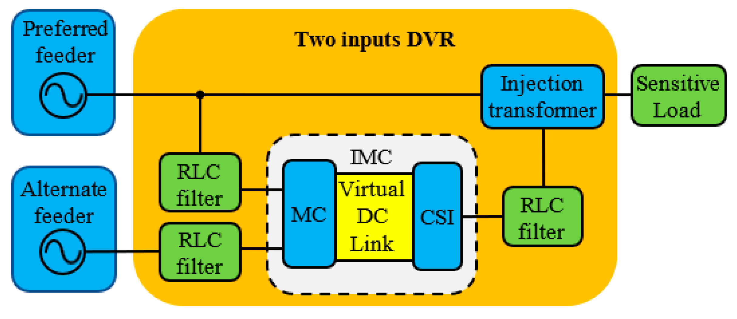
Under these considerations, the proposed system employs two independent distribution feeders to provide power to the DVR as in the case of the CPP. The schematic diagram of the DVR powered by two independent power grids is shown in Figure 2. The DVR consists of an MC with two inputs, a virtual DC-link, a CSI, an injection transformer, and Resistor-Inductor-Capacitor (RLC) filters at the input and output terminals. Figure 3 illustrates the topology of the MC, the CSI and the filters.
The PF supplies energy to the sensitive load. Consequently, the DVR must protect the load from any disturbances that may occur in the feeders. In practice, it is very rare that all independent distribution feeders suffer disturbances at the same time. Therefore, when a fault occurs in the PF, the DVR compensates for the disturbance by taking energy from both feeders and injects it into the grid to maintain the nominal voltage values at the load terminals. If the PF presents a deep and long-term sag, the MC extracts most of the energy from the AF that is operating under normal conditions and transfers it to the virtual DC-link. In order to synthesize the voltage that would be injected in the PF, the inverter takes the available energy in the virtual DC-link.
As mentioned above, the CPP consists of a reconfiguration device (STS), a compensation device (DVR), and a sensitive load. If there is a fault in one of the feeders, the STS feeds the load with the feeder without failure; in addition, the DVR guarantees the compensation of any disturbance and ensures a stable voltage in the load. In contrast, the proposed DVR can take power from the two feeders simultaneously and also perform disturbance compensation present in the feeders and ensure a stable voltage in the load. In this way, the proposed DVR can replace the STSs and DVRs conventionally used in the CPP.
The main characteristics of the proposed topology are:
- Utilizes a MC instead of two conventional converters.
- Integrates two electrical feeders to the DVR.
- Substitutes the DC-link capacitor for a virtual DC-link.
- The range of compensation capacity is extended without the need for an energy storage system.
- The proposed DVR can replace the STSs and DVRs conventionally used in the CPP.
3. CSI Space Vector Modulation
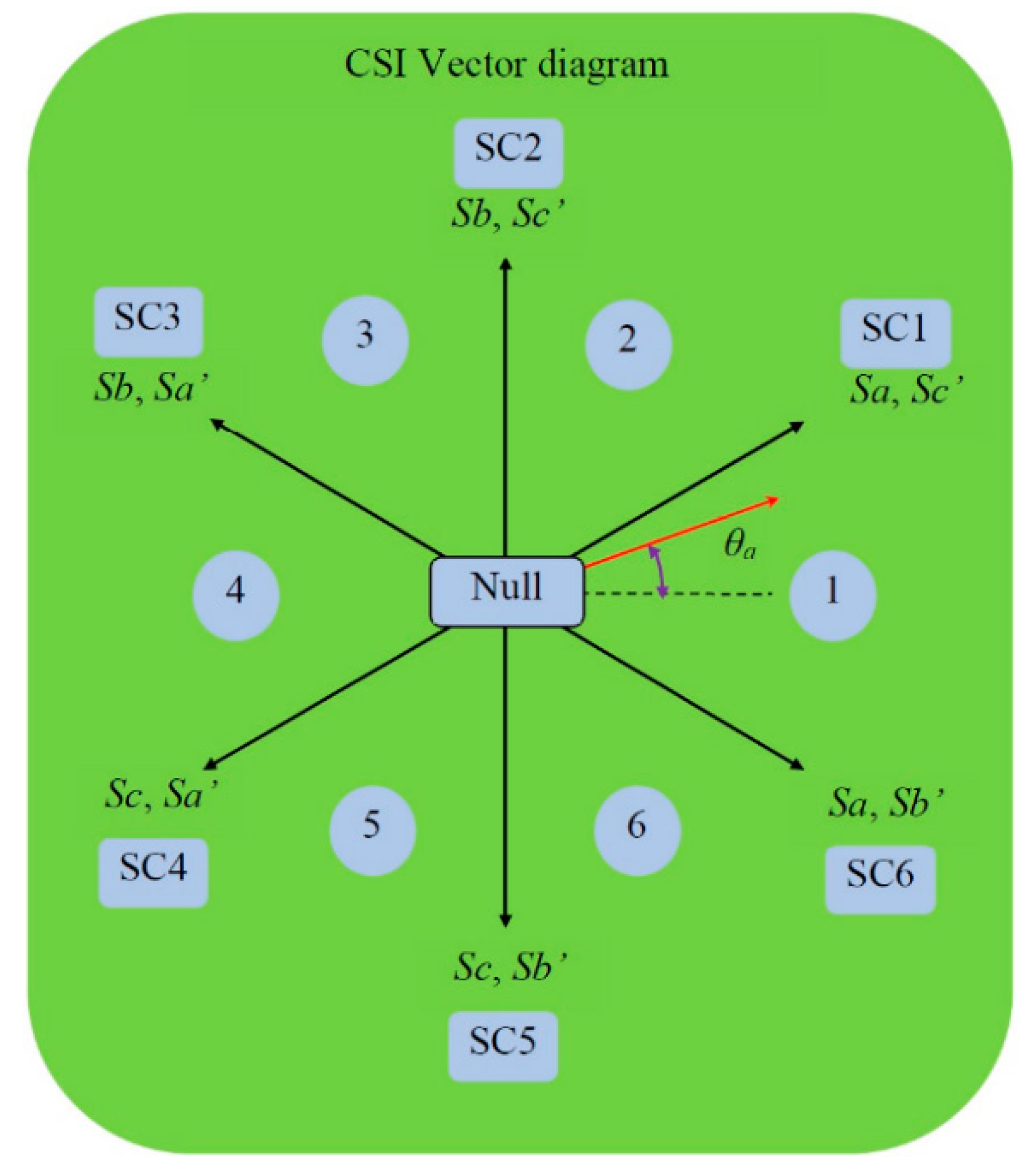
The CSI takes energy from the virtual DC-link to build the voltages that would be injected to the load. To obtain the proper voltages, the switching elements of the CSI must turn on and off in a suitable sequence. For this, the space vector pulse width modulation technique is suitable. This technique has been widely adopted to provide trigger signals to switching elements of inverters in DVRs [28,29,30,31]. The vector representation in the complex space of the active states utilized by the CSI to form the desired voltage is shown in Figure 4.
Considering sextant 1, it has the range −π/6 ≤ θa ≤ π/6. This sector is delimited by the active State of Commutation (SC) SC6 and SC1 that correspond to the voltages vab and vac, respectively. In this way, the line voltages are obtained from the virtual DC-link by commuting the switches Sa, Sb′ and Sa, Sc′. The phase orientation of the CSI output voltages is synchronized with the difference between the reference voltages phase angle and the voltages phase angle measured in the load. The three phase output voltages are defined as
where Vom is the amplitude of the output voltages; and θa, θb and θc are the phase angles.
When the load reference voltages and the line voltages are in phase, the duty cycles do1 and do2 for switches Sb′ and Sc′ in sextant 1 are determined by,
do1 and do2 can be calculated similarly for the other five sextants. For a detailed explanation, see [21] and [22]. The voltage in the virtual DC-link in sextant 1 is determined by
where vabref and vacref are the reference voltages for the load voltages vab and vac, respectively. The voltage in the virtual DC-link in the other five sextants is calculated in a similar way. In [21,22] two energy generators were integrated into the electric network; therefore, the reference voltages were the electric network voltages. In contrast, in this work, the nominal values of the load establish the load reference voltages, and the voltage in the DC-link is calculated with the load reference voltages.
4. Modified Carrier Based PWM Algorithm for the MC
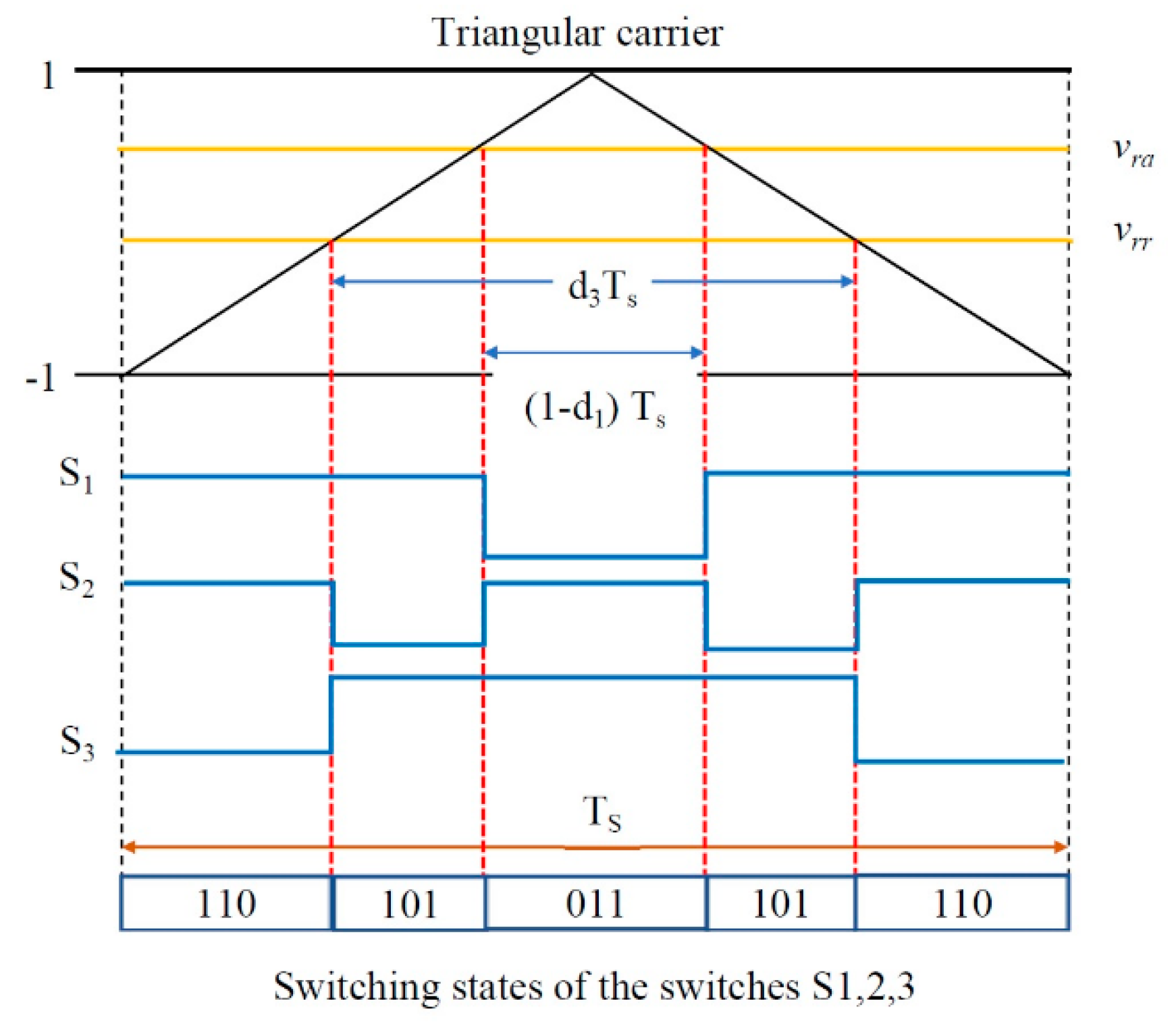
The MCB-PWM implemented for MC modulation employs two sets of reference signals that share a triangular carrier signal. One set of the reference signals corresponds to the PF and the other to the AF. The first set of signals is placed above the second set. It is worth mentioning that in [21,22], a triangular signal with variable slopes was used as a carrier signal, while in this work a triangular signal with constant slopes with a frequency equal to twice the ramp frequency used in the CSI pulse width modulation (PWM). The modification in the triangular carrier signal facilitates the implementation of the triangular carrier and allows the filters at the entrance of the MC to be smaller. In addition, the triangular carrier with constant slopes contributes to the feeders’ current waveforms being sinusoidal.
Figure 5 shows the PWM process implemented for generating the trigger signals for an MC branch. The trigger signals of switches S1 and S3 are generated by comparing the upper and lower reference signals with the triangular carrier signal. The trigger signal S2 is generated with the logical operator XOR between S1 and S3. The relationships for the trigger signals can be set as follows
where vra and vrr are the upper and lower modulation reference signals that corresponds to phase a of the preferred feeder and phase r of the AF. vtri is the triangular carrier signal. d1 and d3 are the duty cycles for switches S1 and S3. The reference signals are given by
where mi1 and mi2 are the modulation indices, ω1 and ω2 are the angular frequencies, θa and θr are the phase angles of the upper and lower input voltages, and Voff1 and Voff2 are the compensation variables utilized to improve the modulation indices, which are given by,
finally, Voffup and Voffdown are the offset signals, up and down, that prevent the crossing between the reference signals sets.
5. DVR Control Algorithm
The control objectives of this algorithm are the following:
- Ensure that the DVR provides adequate energy to the load for its compensation.
- Have a good tracking of the input currents.
- Achieve a unit power factor.
The presented modulation scheme produces currents close to the sinusoidal waveform at the input terminals of the converter, in addition to carrying out adequate load voltage compensation. By implementing the proposed control loop, the converter delivers the necessary energy to the load with a good dynamic response. It is worth mentioning that the MC topology considered allows for the control of the power factor at the terminals of the two feeders.
For practical applications, the following scenario should be considered. There are two feeders; the PF and the AF. The PF supplies energy to one of the inputs of the DVR and the load; the AF feeds the other DVR input. The DVR takes energy from the two feeders to keep the load voltage at its nominal value. When a balanced or unbalanced voltage sag occurs in the PF, there is also a variation in the load voltage. Then, the DVR demands energy from both feeders to compensate for the voltage in the load for as long as necessary. When there is no short-term disturbance in the electrical grid but there is voltage imbalance or harmonics distortion present in the supply voltages, the restorer can cope with these disturbances; in this way, the operating time of the DVR is optimized.
In this topology, the control algorithm is divided into two parts that are synchronized with each other; the control of the CSI and the control of the MC.
5.1. CSI Control Algorithm
Steady-state sinusoidal voltages and currents in the load terminals are guaranteed by the proposed modulation scheme. Additionally, a unity power factor can be achieved through the modulation scheme implemented for the CSI. Under the presence of voltage disturbances in the PF such as sags, swells, voltage imbalance and harmonic distortion, the energy in the load can be compensated in an efficient way in the dq reference frame. Figure 6 shows the structure of the control algorithm implemented in the CSI in order to inject the adequate compensation voltages to mitigate these disturbances.
Due to the nature of this application, the control algorithm of the CSI was modified in the following way; instead of measuring the mains voltage for synchronization purposes [21,22], the load voltage is measured and compared with a reference load voltage to obtain the difference between the voltages and to carry out an adequate compensation of the disturbances. In this application, the input signals for the control algorithm are: (a) Load voltages and (b) reference load voltages. Both voltages are acquired to provide phase angle information (θL and θref) in order to implement ABC-dq reference frame transformations and to determine the active component of each of the voltages: dL and dref.
The load voltage active component dL is compared whit the reference voltage active component dref to determine if the disturbance represents a sag or a swell. Based on this information, the reference phase angle is adjusted to obtain the angle, θsect. As can be seen in Figure 4, this angle describes the phase orientation of the voltage vectors that are required for disturbance compensation in the complex space.
The phase angle θsect determines the corresponding sextant in the complex space. The switching functions do1 and do2 are calculated in each sextant utilizing (2). The CSI PWM generates the trigger signals by comparing the switching functions do1 and do2 with a sawtooth signal. To synthesize the appropriate line voltages, the CSI switches that turn on and off are determined by the sextant defined by the angle θsect.
On the other hand, for synchronization purposes between the CSI and the MC, the control algorithm also generates the triangular carrier signal for the MC modulation and calculates the voltage at the virtual DC-link. The triangular carrier signal is built in the CSI PWM. The voltage calculation in the virtual DC-link is carried out through (3) and directly depends on the voltages between phases of the load reference, the switching functions do1 and do2, and the sextant related to the angle θsect.
5.2. MC Control Algorithm
The modulation scheme of the MC guarantees that the voltage and current waveforms at two input terminals are sinusoidal. The control loop provides a good monitoring of input currents and guarantees a unit power factor in the feeders.
The MC integrates the PF and the AF to the DVR and acquires the energy from both feeders to supply energy to the CSI through the virtual DC-link. Figure 7 shows the control and modulation scheme of the MC.
In this figure, it is shown that the voltages of the PF are measured to obtain information of the phase angle θ1 in the rotary reference frame. This angle is required to implement the abc–dq transformation of the measured currents to ensure that the d-axis of the currents is aligned with the vector of the PF voltages. In order to have a unit power factor, the reference reactive current is made equal to zero; *iq1 = 0. Two proportional-integral (PI) controllers are used to control the active current and the reactive current, respectively. After the control process, a three-phase set of modulation references for the PF is obtained by performing the dq–abc transformation, synchronized through the angle θ1. This set of reference signals is divided by the voltage of the virtual DC-link, calculated in the control algorithm of the CSI. At this point, the calculated virtual DC-link voltage is utilized to achieve an efficient energy transfer and fulfills two important functions: (a) It ensures that MC input voltages and currents are sinusoidal, and (b) it ensures that the virtual DC-link voltage is the adequate for the compensation of the PF voltages. The offset voltage Voffup is added to the set of three-phase modulation references of the PF in order to shift it upwards and prevent it from crossing with the set of modulation references of the AF.
The control algorithm for the AF is almost the same as that of the PF; the only difference is that the three-phase set of modulation references of the AF is traversed downwards, subtracting the offset voltage Voffdown.
The design and tuning of the PI controllers are carried out using the experimental Ziegler–Nichols closed loop method.
The MC PWM technique compares the PF reference signals (vref1) and the set of references of the AF (vref2) with the triangular carrier constructed in the CSI PWM to generate the trigger signals for the MC switches. The on and off times for switches S1, S4 and S7 are obtained by comparing the set of references of the PF (vref1) with the triangular carrier signal in the MC PWM. In the same way, the on and off times for switches S3, S6 and S9 are obtained when comparing the triangular carrier signal with the set of references of the AF (vref2). The ON and OFF signals for switches S2, S5 and S8 are obtained with the logical operator XOR as follows; S2 = (S1) XOR (S3).
By using the proposed topology controlled by the modified algorithms presented, it is possible to compensate deep and long-term sags, swells, interruptions, voltage imbalance and harmonic distortion. In addition, the proposed modified methodology has additional advantages such as:
- The energy storage capacity to mitigate deep and long-term sags is no longer a limitation due to the integration of the AF that provides the energy for as long as necessary.
- There are no energy storage elements in the DC-link. Therefore, the energy transfer between input and output terminals of the DVR is spontaneously balanced, and it is not necessary to measure the DC-link voltage for control purposes since there is no energy storage element.
- Under this scheme, the MC behaves as two Voltage Source Converters (VSC) and integrates two distribution grids to the DVR utilizing only a unified control algorithm. Under a conventional scheme, two VSCs would be needed, as would a controller for each of them.
- In this sense, the modified control algorithm for the DVR presented in this paper is more compact compared to the control algorithms used in conventional two-stage AC–DC–AC converters with energy storage elements.
6. Simulation Results and Discussion
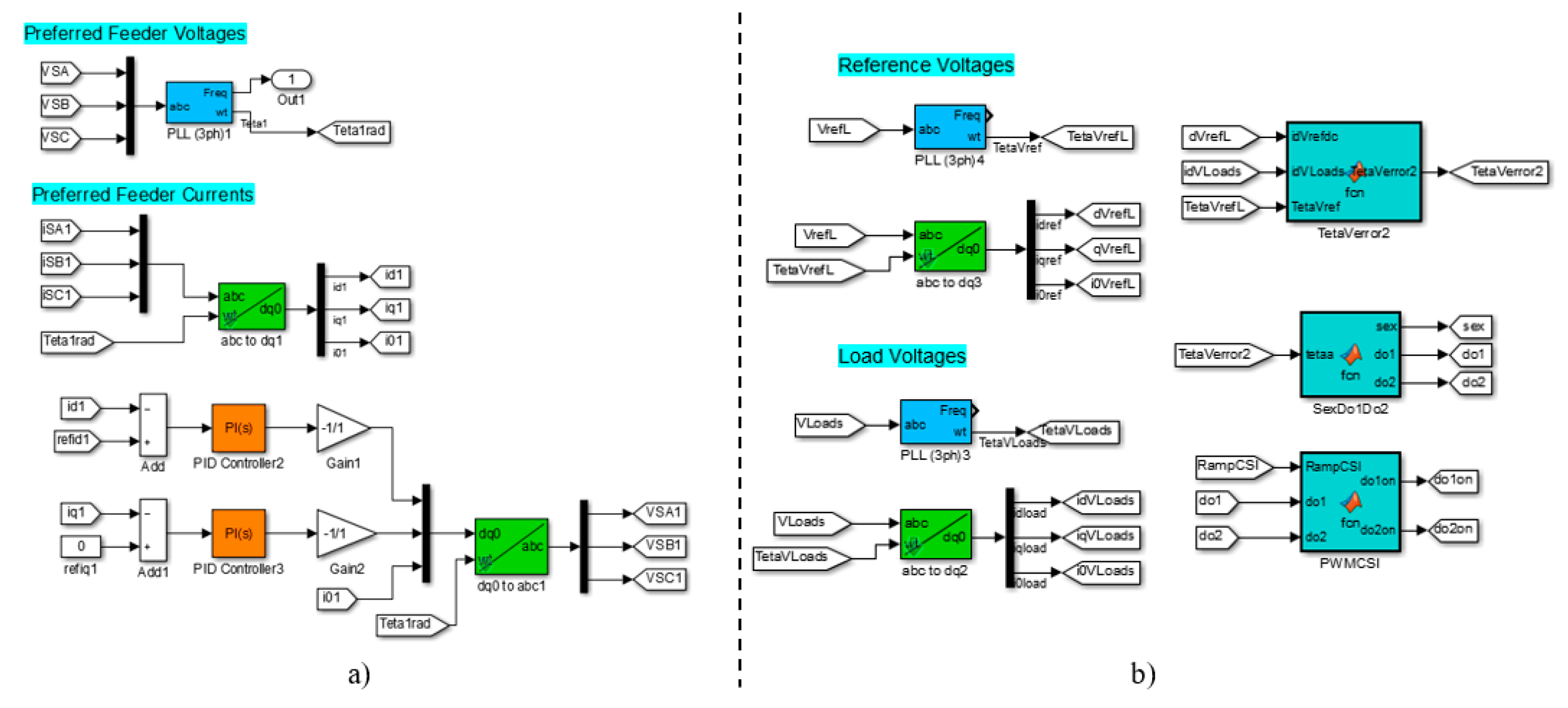
To validate the behavior of the proposed topology, the modulation schemes and the proposed DVR control algorithm, the complete system was implemented on the MATLAB R2015b (64 bits)/Simulink Version 8.6 platform, and the SimPowerSystems library was used. Figure 8 shows the real model implemented in Simulink corresponding to the proposed DVR of Figure 2. Figure 9a,b illustrates the models of the generation of the PF reference voltages and the CSI control algorithm, respectively.
The load values and the input and output filters are shown in Table 1. The purpose of the DVR input and output filters is to attenuate the high frequency harmonics produced by the high frequency switching of the MC and CSI switches. In this way, the values presented in this table determine the bandwidth of the low pass filter used. The system parameters were as follows:
- Preferred Feeder 100 Vp 0 Hz
- Alternated Feeder 100 Vp 60 Hz
- Load reference voltage 100 Vp 60 Hz
- CSI Switching frequency 3.6 KHz
- MC Switching frequency 7.2 KHz
The gains of the PI controllers for the active and reactive current of the two feeders were as follows: Kp = 30, Ki = 0.001.
The behavior of the proposed DVR was analyzed for the following study cases:
- Case 1: Voltage Sag.
- Case 2: Voltage interruption.
- Case 3: Voltage Swell.
- Case 4: Unbalanced sag.
- Case 5: Voltage Harmonics.
For these simulations, it is considered that the AF was stable and operated at the same frequency as the PF. For simulation purposes, the PF and the AF will be called the critical grid and neighbor grid, respectively.
6.1. Case 1: Voltage Sag
A sag is defined as the decrease in the rms value of the supply voltage, between 0.1 and 0.9 p.u., at the feeding frequency and with a duration from 0.5 cycle to 1 min.
In this first study case, the behavior of the proposed DVR when there is a balanced deep sag in the critical grid was evaluated. The voltage sag was simulated by considering that the peak voltage amplitude of all phases of the critical grid were reduced from 100 to 40 Vp during 100 ms. The voltages and currents waveforms of the system are shown in Figure 10 and Figure 11 respectively. The behavior of the system without DVR is shown in Figure 12.
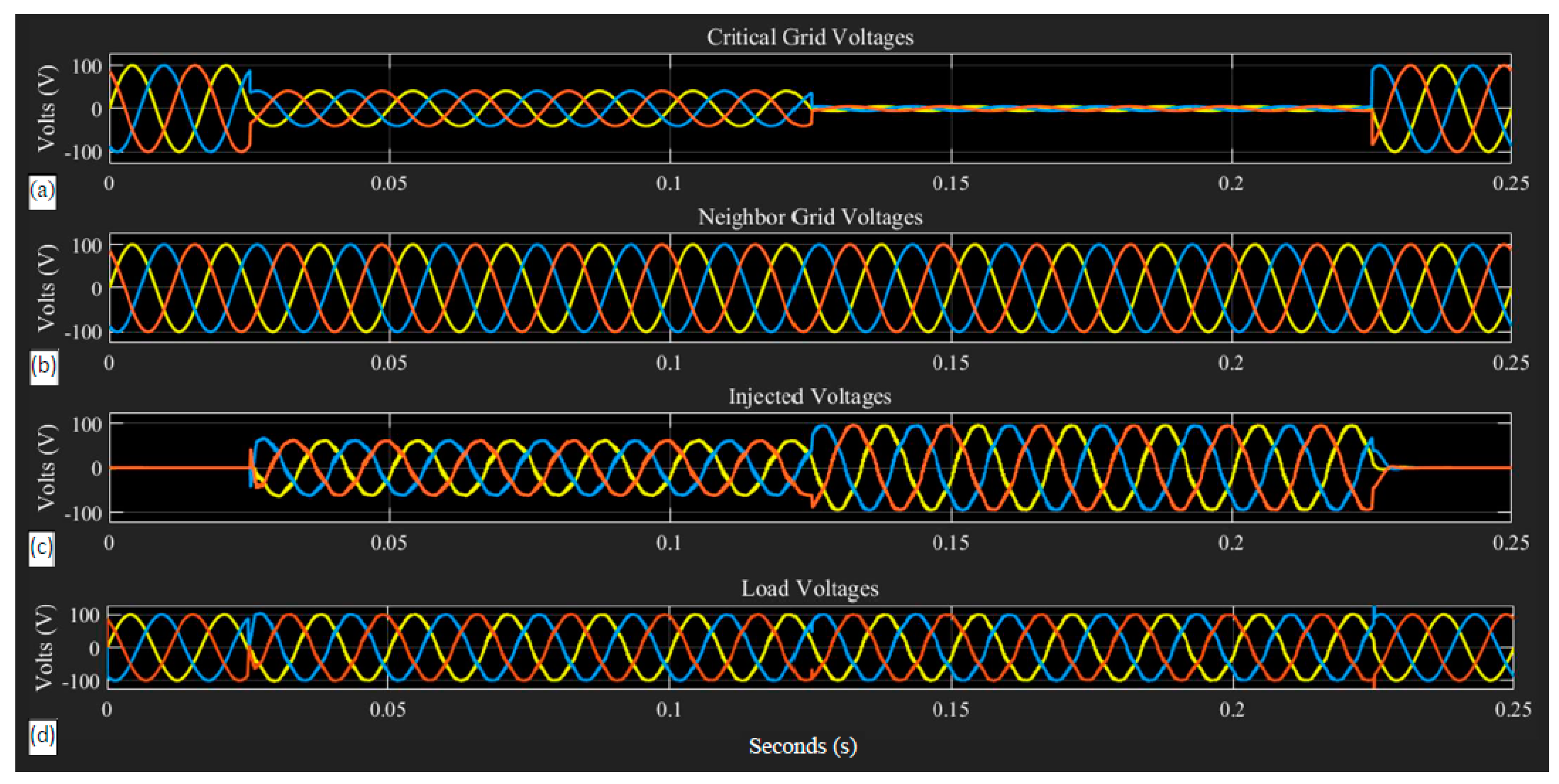
Figure 10 shows the voltages measured in the system that includes the DVR. The sag of 60% was applied in the critical grid in the time interval from 25 to 125 ms, as shown in Figure 10a. The voltage in the neighbor grid remained stable throughout the simulation, as can be seen in Figure 10b. When the fault occurred in the critical grid, the DVR injected a compensation voltage which was added to the critical grid voltage to keep the load voltage practically undisturbed; Figure 10c,d. Figure 10 shows the effectiveness of the DVR to operate confronting this type of disturbance.
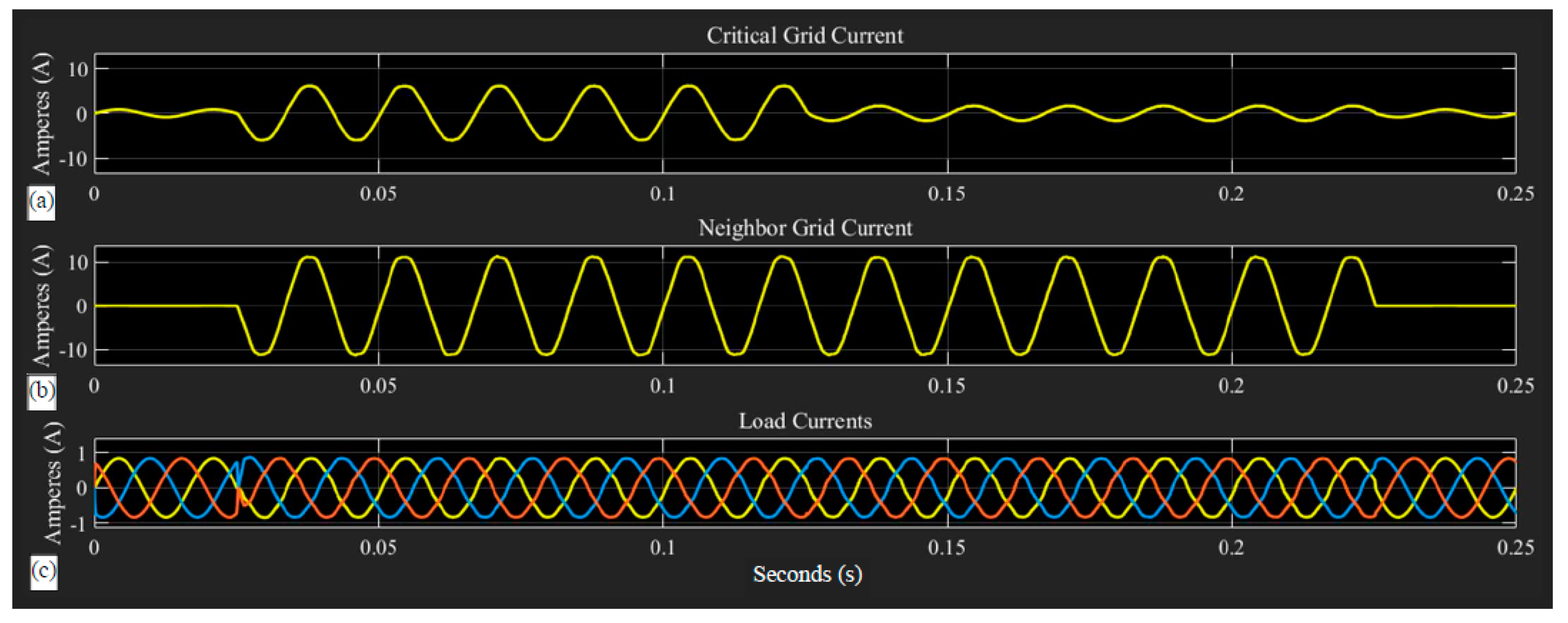
Figure 11 shows the waveforms of system currents, namely the currents demanded to the critical grid and the neighbor grid, and the current consumed by the load. In Figure 11, it can be seen that before the sag, the current in the neighbor grid was equal to zero, and that the load current was stable all the time.
When the sag occurred, the MC took energy from the two feeders. Figure 11 shows how the amplitude of the currents increased during the sag. However, the amplitude of the neighbor grid current was greater than the amplitude of the critical grid current. In this case, the DVR absorbed more energy from the neighbor grid to compensate for the sag in the critical grid.
In order to compare the performance between the proposed two-input DVR and a one-input DVR in sags compensation, consider Figure 10 and Figure 13 taken from [27]. At the beginning of the sag, the proposed two-input DVR (Figure 10) responded quickly, and the load voltage showed a slight flicker. Figure 10 shows that at the end of the interruption, the injection voltage of the proposed two-input DVR quickly tended to zero, and the load voltage showed a spike. In counterpart, Figure 13a shows a spike in the one-input DVR waveforms at the beginning of the sag. At the end of the sag, it was possible to observe a half-cycle oscillation in the injection voltage of the one-input DVR and a slight distortion in the load voltage.
6.2. Case 2: Voltage Interruption
An interruption occurs when the supply voltage or load current decreases to less than 0.1 p.u. for a period of time less than 1 min.
In this section, the behavior of the proposed DVR against a voltage interruption is studied. To simulate a voltage interruption, the peak voltage amplitude of all phases of the critical grid were reduced from 100 to 5 Vp during 100 ms. The waveforms of system voltages and currents are shown in Figure 10 and Figure 11, respectively. In the time interval from 125 to 225 ms, the voltage interruption in the critical grid was simulated, as shown in Figure 10a.
In this case, to keep the voltage stable in the load, the DVR transferred the necessary energy from the neighbor grid to the critical grid. The voltage injected by the DVR to the critical grid is shown in Figure 10c; this voltage had an amplitude of 0.95 p.u. Figure 10d shows that the DVR was able to maintain the load voltage at its nominal value despite the voltage interruption.
Figure 10 shows the system currents waveforms. In this case, the current in the neighbor grid was higher than the current in the critical grid; this means that the DVR took all the necessary energy from the neighbor grid to compensate for the voltage interruption in the critical grid. As in the previous case, the current in the load remained constant during the voltage interruption, as seen in Figure 10c.
The behavior of the system without DVR is shown in Figure 12. The load voltages and currents made evident the good performance of the proposed DVR, even during extreme conditions in voltage drop.
6.3. Case 3: Voltage Swell
A swell is defined as an increase in the rms value of voltage or current of around 1.1 to 1.8 p.u., with a duration from 0.5 cycles to 1 min.
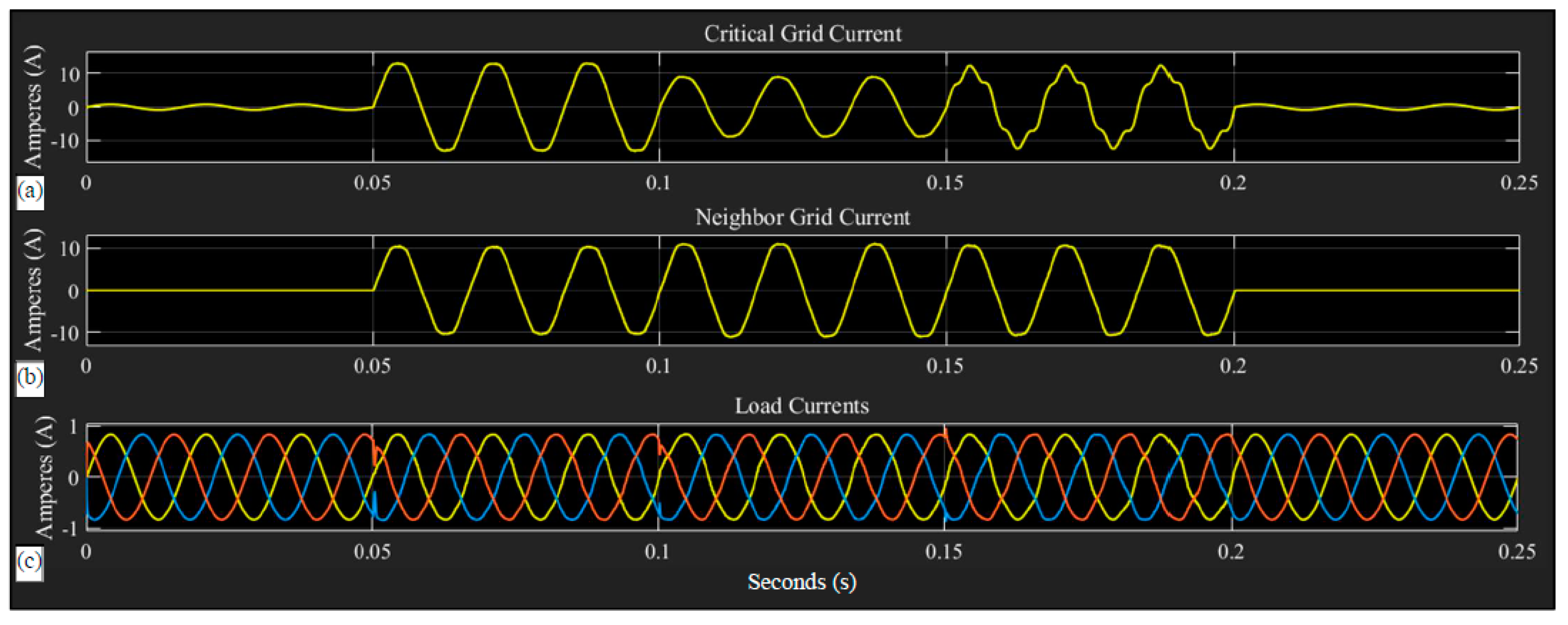
In this third study case, the DVR operation was verified when the system was subject to a voltage swell. System voltage waveforms are shown in Figure 14. The currents waveforms are shown in Figure 15 and the behavior of the system without DVR is shown in Figure 16. The simulation of the voltage swell condition was achieved by considering that the peak voltage amplitude of all phases of the critical grid rose from 100 to 130 Vp during 50 ms from the time period of 50 to 100 ms. While Figure 14a shows a voltage swell in the critical grid, in Figure 14b, it is possible to see that the neighbor grid remained stable. The DVR injected phase voltages had an amplitude of 30 Vp with a phase shift of 180 degrees with respect to the phase angles of the critical grid voltages. In this way, the swell was compensated appropriately. As the load voltage remained invariant during the simulation (Figure 14d), it can be concluded that the proposed DVR can satisfactorily compensate for the presence of swells in the critical grid.
The waveforms of system currents are shown in Figure 15. During the disturbance, the MC demanded current from both feeders, as shown in Figure 15a,b, and transferred this energy to the virtual DC-link of the DVR. The CSI utilized the energy from the virtual DC-link and synthesized the compensation voltages, as shown in Figure 14c. The simulation results presented in Figure 14d and Figure 15c show the effectiveness of the proposed DVR in maintaining invariant load voltages and currents despite the presence of voltage swells in the critical grid.
Figure 14 and Figure 17a (Taken from [27]) show the waveforms of the proposed two-input DVR and the DVR presented in [27] in the compensation of a swell. The two DVRs responded immediately when the disturbance occurred. Both generated the corresponding injection voltage to compensate for the swell. The injection voltage of the DVR presented in [27] presented a slight distortion when the disturbance occurred. On the other hand, the injection voltage generated by the proposed DVR showed a voltage spike. The waveforms of Figure 17a show a spike in the load voltage when the disturbance occurred, and the waveforms of the proposed DVR (Figure 14) showed a flicker. In the time interval that the disturbance was present, the DVR presented in [27] presented a slight increase of 4%, and the proposed two-input DVR maintained the load voltage at its nominal values. At the end of the swell, Figure 17a shows that the injection voltage took approximately half a cycle of the fundamental to drop to zero, and the DVR proposed here took approximately a quarter of the fundamental cycle.
6.4. Case 4: Unbalanced Sag
In this study case, the ability of the proposed DVR to compensate unbalanced voltage sags was evaluated. The voltage disturbance was applied in the critical grid modifying the phase voltage magnitudes as follows: Phase a; 80 V peak that represented a 20% voltage reduction with respect to its nominal value; Phase b; a 60 V peak that represented a 40% voltage reduction with respect to its nominal value; and Phase c; a 40 V peak that represented a 60% voltage reduction with respect to its nominal value.
The unbalanced sag in the critical grid is simulated in the time interval from 100 to 150 ms as shown in Figure 14a. The neighbor grid voltages remained undisturbed during the fault, as shown in Figure 14b. In this case, the DVR extracted energy from both feeders to mitigate the disturbance. The current in the neighbor grid was greater than the current in the critical grid, as is illustrated in Figure 14a,b, which means that the DVR took most of the active power from the neighbor grid and transferred it to the critical grid to compensate for the unbalanced sag. Figure 14c shows the voltage waveforms synthesized by the DVR to inject them into the critical grid in order to mitigate the disturbance. The amplitude of the injected voltages in phases a, b, and c of the critical grid were 20, 40, and 60 V, respectively. As in previous study cases, the DVR was able to keep load voltages in its nominal values during the period of time the unbalance sag lasts; Figure 14d and Figure 15c.
Figure 13b and Figure 14 show the performance in the presence of an unbalanced sag to the DVR presented in [27] and the two-input DVR proposed in this paper, respectively. At the beginning of the unbalanced sag, both DVRs responded quickly. However, the load voltage in Figure 13b [27] shows a slight distortion. On the other hand, Figure 14 shows a small flicker in the load voltage at the beginning of the unbalanced sag. In the time interval that the disturbance occurs, both DVRs performed the compensation. However, the load voltage shown in Figure 13b continued to show a slight imbalance. In counterpart, the load voltage shown in Figure 14 was maintained at the nominal values of the load. Finally, when the grid voltage returned to its nominal values, the DVR presented in [27] presented a settlement of approximately one fundamental cycle (Figure 13b), while the two-input DVR presented here achieved it in much less time (Figure 14).
6.5. Case 5: Harmonic Distortion
Harmonic distortions present in supply voltages have a negative impact on the electrical network and on sensitive loads. In this final study case, the behavior of the proposed DVR facing the presence of voltage harmonics in the critical grid was analyzed. To carry out the simulation, a fifth harmonic with an amplitude of 20% with respect to the fundamental component was added in every critical grid phase voltage.
The harmonic distortion in the critical grid was simulated in the time interval from 150 to 200 ms, as shown in Figure 14a. The neighbor grid voltages remained invariant during the disturbance, as can be seen in Figure 14b, whilst Figure 15 exhibits the system currents waveforms. In this case, the presence of the fifth harmonic also affected the critical grid current waveform, Figure 15a. In order to compensate for the presence of harmonic distortion in the critical grid voltages, the DVR utilized the energy coming from both distribution feeders. The MC transferred the energy to the virtual DC-link, and the CSI constructed the compensation voltages. In this case, it is clear from Figure 14c that compensation voltages generated by the DVR can eliminate the harmonic components present in the critical feeder. As corroborated by Figure 14d and Figure 15c, the proposed DVR was capable of performing the voltage active filter function.
For the purpose of comparing the load voltages with and without the DVR, Figure 12 and Figure 16 present the signals measured in the system without the compensator. Finally, by comparing the load voltage and current waveforms from Figure 12 and Figure 16 with Figure 10, Figure 11, Figure 14 and Figure 15, a remarkable performance of the DVR in applications related to PQ disturbances compensation it is evident.
Figure 14 shows the behavior of the two-input DVR proposed in harmonic compensation, and the performance of the DVR presented in [24] is illustrated in Figure 17b. The feeder in Figure 14 showed the presence of the fifth harmonic, and the feeder in Figure 17b contained the third and seventh harmonics. Both DVRs showed good performance in harmonic compensation. However, in the figures, it can be seen that the DVR presented in [24] showed slight oscillations in the amplitude of the load voltage, unlike the proposed two-input DVR that kept the load voltage stable in harmonic compensation.
6.6. Summary of the Results
The results obtained from the simulations and their respective discussion make it possible to conclude that the proposed DVR is able to compensate different types of disturbances in a feeder that supplies energy to a sensitive load. In the particular case where voltage sags and interruptions are presented in the network, the energy transfer from the neighbor grid to the critical grid widely extended the DVR range of compensation, and it did not depend on expensive energy storage devices.
The effect of the modifications imposed on the modulation schemes and control algorithms were manifested in the behavior of the proposed DVR. The advantages and characteristics of the modified modulation scheme and the algorithm control are summarized as follows:
- The proposed control algorithm allows the DVR to generate the appropriate voltages to perform the compensation of different disturbances in the input voltages.
- The modified control algorithm for the DVR presented in this paper is more compact compared to the control algorithms used in conventional two-stage AC–DC–AC converters with energy storage elements.
- Unlike other works, the voltage calculated in the DC-link was obtained according to the reference voltages and the switching functions of the CSI-PWM.
- The DC-link calculated voltage allows for the synchronization between the MC and the CSI, thus achieving an optimal energy transfer between the MC and the CSI. In addition, it contributes to the feeders’ current waveforms being sinusoidal.
- The use of a triangular carrier signal of constant slopes instead of a triangular signal of variable slopes facilitates its implementation and contributes to the current waveforms of the feeders being sinusoidal. This signal also joins in to the synchronization between the MC and the CSI.
- The size of the filters at the MC input is reduced because the MC-PWM triangular carrier signal has twice the frequency of the CSI PWM ramp.
The incorporation of the two inputs to the MC in the compensator topology resulted in a multifunctional behavior of the DVR. The simulation results show the efficiency and validity of the proposed topology.
7. Conclusions
In this paper, the performance of a DVR based on the MC with two three-phase inputs was analyzed. The proposed topology was evaluated in applications related to most common PQ disturbances compensation. The control scheme utilized for the DVR has the advantage of being more compact compared to DVR control schemes based on conventional AC–DC–AC two-stage converters. An important feature of the proposed DVR is its ability to transfer energy from an AF to inject it into the PF in a CPP. This operational characteristic allows for the replacement of the STS and DVR conventionally used by the proposed DVR. In addition, the compensation range of the DVR is extended, and its general behavior improves, making it an attractive solution to deal with several disturbances affecting PQ energy, including extreme conditions like deep and long-term sags and voltage interruptions.
On the other hand, the proposed DVR topology presents many development opportunities in future research. Among them, the following can be mentioned:
- The implementation of a prototype for experimental tests.
- The DVR application proposed as an interface in microgrids.
- Another interesting application may be the compensation of disturbances in hybrid microgrids where a device for the integration of microgrids is necessary.
- A reconfiguration of networks and compensation of disturbances in smart grids also presents an interesting challenge
Author Contributions
Conceptualization, S.C.Y.-C.; formal analysis, G.C.-V. and J.M.L.-G.; investigation, S.C.Y.-C.; methodology, S.C.Y.-C.; supervision, G.C.-V. and J.M.L.-G.; validation, S.C.Y.-C., G.C.-V. and J.M.L.-G.; visualization, S.C.Y.-C.; writing—original draft, S.C.Y.-C.; writing—review & editing, G.C.-V. and J.M.L.-G.
Funding
This research was funded by the Program for Teacher Professional Development (PRODEP) grant number ITESI-008. And The APC was funded by the University of Guanajuato PFCE 2019.
Conflicts of Interest
The authors declare no conflict of interest.
References
- Electric Power Research Institute (EPRI). Power Quality in Commercial Buildings; BR-105018; EPRI: Palo Alto, CA, USA, 1995. [Google Scholar]
- Koval, D.O.; Hughes, M.B. Canadian national power quality survey: Frequency of industrial and commercial voltage sags. IEEE Trans. Ind. Appl. 1997, 33, 622–627. [Google Scholar] [CrossRef]
- Sabin, D.D. An assessment of distribution system power quality. In Elect. Power Res.; 1996; Rep. TR-106294-V2. Available online: https://www.osti.gov/biblio/263014 (accessed on 25 June 2019).
- Hingorani, N. Introducing custom power. IEEE Spectr. 1995, 32, 41–48. [Google Scholar] [CrossRef]
- Pal, Y.; Swarup, A.; Singh, B.A. Review of compensating type custom power devices for power quality improvement. In Proceedings of the 2008 Joint International Conference on Power System Technology and IEEE Power India Conference, New Delhi, India, 12–15 October 2008; pp. 1–8. [Google Scholar]
- Praveena, S.; Kumar, B.S. Performance of custom power devices for power quality improvement. In Proceedings of the 2017 IEEE International Conference on Power, Control, Signals and Instrumentation Engineering (ICPCSI), Chennai, India, 21–22 September 2017; pp. 912–917. [Google Scholar]
- Nielsen, J.G.; Blaabjerg, F. A detailed comparison of system topologies for dynamic voltage restorers. IEEE Trans. Ind. Appl. 2005, 41, 1272–1280. [Google Scholar] [CrossRef]
- Farhadi-Kangarlu, M.; Babaei, E.; Blaabjerg, F. A comprehensive review of dynamic voltage restorers. Int. J. Electr. Power Energy Syst. 2017, 92, 136–155. [Google Scholar] [CrossRef]
- İnci, M.; Büyük, M.; Tan, A.; Bayındır, K.C.; Tümay, M. Survey of inverter topologies implemented in dynamic voltage restorers. In Proceedings of the 4th International Conference on Control, Decision and Information Technologies (CoDIT), Barcelona, Spain, 5–7 April 2017; pp. 1141–1146. [Google Scholar]
- Merchan-Villalba, L.R.; Carreño-Meneses, C.A.; Pizano-Martinez, A.; Zamora-Cardenas, E.A.; Gonzalez-Ramirez, X.; Lozano-Garcia, J.M. Load-side DVR based on matrix converter for deep voltage sags compensation. In Proceedings of the 2017 IEEE International Autumn Meeting on Power, Electronics and Computing (ROPEC 2017), Ixtapa, Mexico, 8–10 November 2017; pp. 1–6. [Google Scholar]
- Zargar, A.; Masoud Barakati, S. A new dynamic voltage restorer structure based on three-phase to single-phase ac/ac matrix converter. In Proceedings of the 20th Iranian Electrical Power Distribution Conference (EPDC2015), Zahedan, Iran, 28–29 April 2015; pp. 234–238. [Google Scholar]
- Garcia-Vite, P.M.; Mancilla-David, F.; Ramirez, J.M. Per-sequence vector-switching matrix converter modules for voltage regulation. IEEE Trans. Ind. Electron. 2013, 60, 5411–5421. [Google Scholar] [CrossRef]
- Daghani, H.; Ghazi, R.; Ghasemabadi, H. Compensating of voltage flicker and disturbance using dynamic voltage restorer based on matrix converter. In Proceedings of the 21st Iranian Conference on Electrical Engineering (ICEE), Mashhad, Iran, 14–16 May 2013; pp. 1–6. [Google Scholar]
- Ramirez, J.M.; Garcia-Vite, P.; Lozano, J.M.; Mancilla-David, F. Dynamic voltage restorers based on AC-AC topologies. In Proceedings of the IEEE Power and Energy Society General Meeting, San Diego, CA, USA, 22–26 July 2012; pp. 1–7. [Google Scholar]
- Lozano, J.M.; Hernandez, M.A.; Ramirez, J.M. An operative comparison of two DVR topologies based on a matrix converter without energy storage. In Proceedings of the IECON 2012—38th Annual Conference on IEEE Industrial Electronics Society, Montréal, QC, Canada, 25–28 October 2012; pp. 6050–6056. [Google Scholar]
- Mohammed, B.S.; Rama Rao, K.S.; Ibrahim, R.; Perumal, N. Application of custom power park to improve power quality of sensitive loads. In Proceedings of the IEEE 5th India International Conference on Power Electronics (IICPE), Delhi, India, 6–8 December 2012; pp. 1–6. [Google Scholar]
- Ghosh, A.; Joshi, A. The concept and operating principles of a mini custom power park. IEEE Trans. Power Deliv. 2004, 19, 1766–1774. [Google Scholar] [CrossRef]
- Seung-Min, S.; Jin-Young, K.; In-Dong, K. New three-phase static transfer switch using AC SSCB. In Proceedings of the 2018 International Power Electronics Conference, Niigata, Japan, 20–24 May 2018; pp. 3229–3236. [Google Scholar]
- Aghazadeh, A.; Noroozian, R.; Jalilvand, A.; Haeri, H. Combined operation of dynamic voltage restorer with distributed generation in custom power park. In Proceedings of the 10th International Conference on Environment and Electrical Engineering, Rome, Italy, 1–7 May 2011; pp. 1–4. [Google Scholar]
- Mahmood, T.; Choudhry, M.A. Application of static transfer switch for feeder reconfiguration to improve voltage at critical locations. In Proceedings of the 2006 IEEE/PES Transmission & Distribution Conference and Exposition: Latin America, Caracas, Venezuela, 15–18 August 2006; pp. 1–6. [Google Scholar]
- Liu, X.; Wang, P.; Loh, P.C.; Blaabjerg, F. A three-phase dual-input matrix converter for grid integration of two ac type energy resources. IEEE Trans. Ind. Electron. 2013, 60, 20–30. [Google Scholar] [CrossRef]
- Kandasamy, V.; Manoj, R. Grid integration of AC and DC energy resources using multi-input nine switch matrix converter. In Proceedings of the 2014 International Conference on Green Computing Communication and Electrical Engineering (ICGCCEE), Coimbatore, India, 6–8 March 2014; pp. 1–4. [Google Scholar]
- Newman, M.J.; Holmes, D.G.; Nielsen, J.G.; Blaabjerg, F. A dynamic voltage restorer (DVR) with selective harmonic compensation at medium voltage level. IEEE Trans. Ind. Appl. 2005, 41, 1744–1753. [Google Scholar] [CrossRef]
- Tasre, M.B.; Dhole, G.M.; Jadhao, S.S.; Sharma, R.B. A simplified algorithm for sag and harmonic mitigation using DVR. In Proceedings of the 2017 International Conference on Computing, Communication, Control and Automation (ICCUBEA), Pune, India, 17–18 August 2017; pp. 1–6. [Google Scholar]
- Kanjiya, P.; Singh, B.; Chandra, A.; Al-Haddad, K. SRF theory revisited to control self-supported dynamic voltage restorer (DVR) for unbalanced and nonlinear loads. IEEE Trans. Ind. Appl. 2013, 49, 2330–2340. [Google Scholar] [CrossRef]
- Ogunboyo, P.T.; Tiako, R.; Davidson, I.E. Effectiveness of dynamic voltage restorer for unbalance voltage mitigation and voltage profile improvement in secondary distribution system. Can. J. Electr. Comput. Eng. 2018, 41, 105–115. [Google Scholar]
- Tien, D.V.; Gono, R.; Leonowicz, Z. A Multifunctional Dynamic Voltage Restorer for Power Quality Improvement. Energies 2018, 11, 1351. [Google Scholar] [CrossRef]
- Zhan, C.; Ramachandaramurthy, V.K.; Arulampalam, A.; Fitzer, C.; Kromlidis, S.; Bames, M.; Jenkins, N. Dynamic voltage restorer based on voltage-space-vector PWM control. IEEE Trans. Ind. Appl. 2001, 37, 1855–1863. [Google Scholar] [CrossRef]
- Rosli, O.; Rahim, N.A. Implementation and control of a dynamic voltage restorer using Space Vector Pulse Width Modulation (SVPWM) for voltage sag mitigation. In Proceedings of the 2009 International Conference for Technical Postgraduates (TECHPOS), Kuala Lumpur, Malaysia, 14–15 December 2009; pp. 1–6. [Google Scholar]
- Prakash, N.; Jacob, J.; Reshmi, V. Comparison of DVR performance with Sinusoidal and Space Vector PWM techniques. In Proceedings of the 2014 Annual International Conference on Emerging Research Areas: Magnetics, Machines and Drives (AICERA/iCMMD), Kottayam, India, 24–26 July 2014; pp. 1–6. [Google Scholar]
- Zhan, C.; Arulampalam, A.; Jenkins, N. Four-wire dynamic voltage restorer based on a three-dimensional voltage space vector PWM algorithm. IEEE Trans. Power Electron. 2003, 18, 1093–1102. [Google Scholar] [CrossRef]
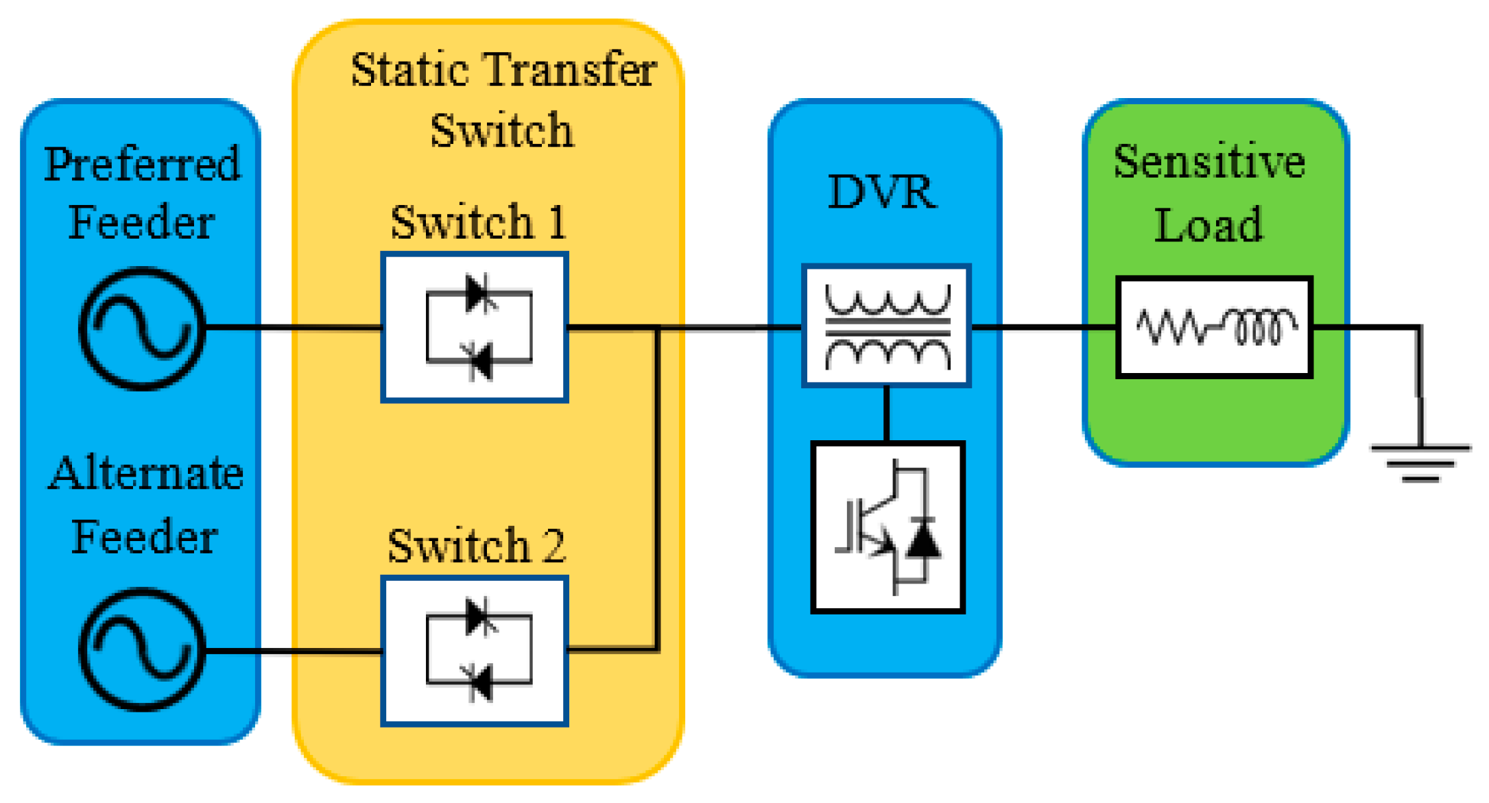
Figure 1.
Custom power park (CPP) conceptual representation with two feeders, static transfer switch (STS), dynamic voltage restorer (DVR) and a sensitive load.
Figure 1.
Custom power park (CPP) conceptual representation with two feeders, static transfer switch (STS), dynamic voltage restorer (DVR) and a sensitive load.

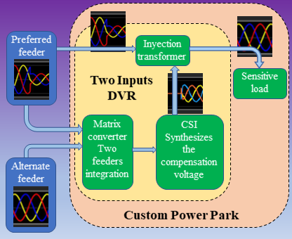
Figure 2.
Schematic diagram of the proposed DVR fed with two independent feeders. The proposed DVR can replace the STS and traditional DVR used in the CPP.
Figure 2.
Schematic diagram of the proposed DVR fed with two independent feeders. The proposed DVR can replace the STS and traditional DVR used in the CPP.

Figure 3.
Matrix converter (MC), current source inverter (CSI) and RLC filters topologies.

Figure 4.
Space vector representation of the CSI.

Figure 5.
Pulse width modulation (PWM) for one branch of the MC.

Figure 6.
CSI control algorithm.

Figure 7.
MC control algorithm and modulation.

Figure 8.
Implemented model in Simulink of the proposed DVR.

Figure 9.
(a) Models of the generation of the reference voltages of the preferred feeder (PF). (b) Model of the CSI control algorithm.
Figure 9.
(a) Models of the generation of the reference voltages of the preferred feeder (PF). (b) Model of the CSI control algorithm.

Figure 10.
System voltage signals in sag compensation and voltage interruption.

Figure 11.
System current waveforms. Case 1: Sag of the 60%. Case 2: Voltage interruption of 95%.

Figure 12.
System waveforms without the DVR. Case 1: Sag of the 60% with 40 Vp amplitude; Case 2: Voltage interruption of the 95% with 5 Vp amplitude. (a) Critical grid voltages, (b) load voltages, and (c) load currents.
Figure 12.
System waveforms without the DVR. Case 1: Sag of the 60% with 40 Vp amplitude; Case 2: Voltage interruption of the 95% with 5 Vp amplitude. (a) Critical grid voltages, (b) load voltages, and (c) load currents.

Figure 13.
Simulation results. (a) Balanced voltage sag and (b) unbalanced voltage sag. Top-down waveforms, grid voltage, injected voltage of the DVR and load voltage (Figures taken from [27]).
Figure 13.
Simulation results. (a) Balanced voltage sag and (b) unbalanced voltage sag. Top-down waveforms, grid voltage, injected voltage of the DVR and load voltage (Figures taken from [27]).

Figure 14.
System voltage waveforms. Case 3: Swell of the 30%; Case 4: Unbalanced sag; and Case 5: Voltage harmonics. (a) Critical grid voltages, (b) neighbor grid voltages, (c) injected voltages, and (d) load voltages.
Figure 14.
System voltage waveforms. Case 3: Swell of the 30%; Case 4: Unbalanced sag; and Case 5: Voltage harmonics. (a) Critical grid voltages, (b) neighbor grid voltages, (c) injected voltages, and (d) load voltages.

Figure 15.
System current waveforms. Case 3: Swell of the 30%; Case 4: Unbalanced sag; and Case 5: Voltage harmonics. (a) Critical grid current, (b) neighbor grid current, and (c) load currents.
Figure 15.
System current waveforms. Case 3: Swell of the 30%; Case 4: Unbalanced sag; and Case 5: Voltage harmonics. (a) Critical grid current, (b) neighbor grid current, and (c) load currents.

Figure 16.
System waveforms without the DVR. Case 3: Swell of the 30%; Case 4: Unbalanced sag; and Case 5: Voltage harmonics. (a) Critical grid voltages, (b) load voltages, and (c) load currents.
Figure 16.
System waveforms without the DVR. Case 3: Swell of the 30%; Case 4: Unbalanced sag; and Case 5: Voltage harmonics. (a) Critical grid voltages, (b) load voltages, and (c) load currents.


Table 1.
Simulation parameters of the DVR.
| Quantity/Parameter | Values and Units |
|---|---|
| Capacitors of the input filters | 10 μF |
| Resistance of the input filters | 50 Ω |
| Inductors of the input filters | 2.2 mH |
| Output filter capacitor | 4.7 μF |
| Output filter resistance | 100 Ω |
| Output filter inductor | 25 mH |
| Load resistance | 120 Ω |
| Load inductor | 8 mH |
© 2019 by the authors. Licensee MDPI, Basel, Switzerland. This article is an open access article distributed under the terms and conditions of the Creative Commons Attribution (CC BY) license (http://creativecommons.org/licenses/by/4.0/).
Share and Cite
MDPI and ACS Style
Yáñez-Campos, S.C.; Cerda-Villafaña, G.; Lozano-Garcia, J.M. Two-Feeder Dynamic Voltage Restorer for Application in Custom Power Parks. Energies 2019, 12, 3248. https://0-doi-org.brum.beds.ac.uk/10.3390/en12173248
AMA Style
Yáñez-Campos SC, Cerda-Villafaña G, Lozano-Garcia JM. Two-Feeder Dynamic Voltage Restorer for Application in Custom Power Parks. Energies. 2019; 12(17):3248. https://0-doi-org.brum.beds.ac.uk/10.3390/en12173248
Chicago/Turabian StyleYáñez-Campos, Sergio Constantino, Gustavo Cerda-Villafaña, and Jose Merced Lozano-Garcia. 2019. "Two-Feeder Dynamic Voltage Restorer for Application in Custom Power Parks" Energies 12, no. 17: 3248. https://0-doi-org.brum.beds.ac.uk/10.3390/en12173248
Note that from the first issue of 2016, this journal uses article numbers instead of page numbers. See further details here.