
Dynamic Process Analysis and Voltage Stabilization Control of Multi-Load Wireless Power Supply System


1
School of Electrical Engineering, Shandong University, Jinan 250061, China
2
Shandong Provincial Key Laboratory of Biomass Gasification Technology, Energy Institute, Qilu University of Technology (Shandong Academy of Sciences), Jinan 250353, China
*
Author to whom correspondence should be addressed.
Energies 2021, 14(5), 1466; https://0-doi-org.brum.beds.ac.uk/10.3390/en14051466
Submission received: 19 January 2021
/
Revised: 28 February 2021
/
Accepted: 3 March 2021
/
Published: 8 March 2021
(This article belongs to the Special Issue Research on Wireless Power Transfer System)
Abstract
:At present, wireless power supply technology has gradually attracted people’s attention due to its safety, convenience, and portability. It has become one of the development trends of power supply for future technologies such as electric vehicles. In many engineering applications, inductive wireless power supply systems need to supply power to multiple loads at the same time. Therefore, it is necessary to analyze the dynamic process of the multiload system. This paper first selects the optimal compensation network according to the stable operating conditions of the multiload system. Secondly, in order to classify and describe the movement state of the load in the dynamic process, the simulation model is established on the MATLAB/SIMULINK platform to analyze the influence of the mutual inductance or resistance of any load on the output characteristics of the primary system and other loads. Then, in order to solve the problem of unstable output voltage used by multiple loads entering the same track at the same time or load resistance changes, this paper adopts a secondary side control strategy. The duty cycle of the Buck circuit is adjusted by the fixed frequency PWM sliding mode controller (PWMSMC), so as to realize the independent control of each load. Finally, an experimental platform was established to verify the correctness of the theoretical analysis.
1. Introduction
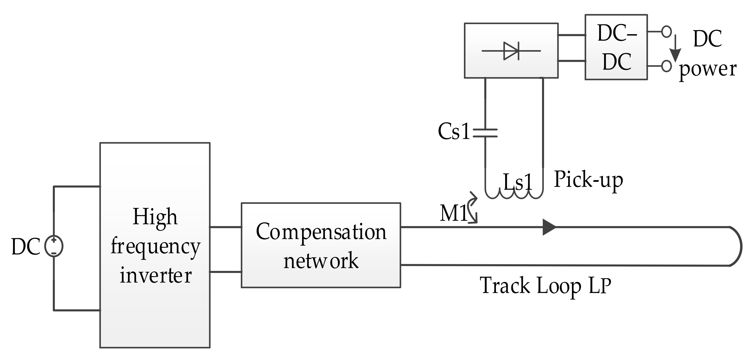
Wireless power transfer (WPT) has become a major technology in modern automation applications because it provides less installation workload, greater flexibility and mobility, and at the same time eliminates the wear and tear of power supply cables [1]. Static wireless charging and wired charging also have problems such as frequent charging, short cruising range, large battery consumption and high cost [2,3]. In this context, dynamic wireless power supply technology emerged. The inductive wireless power supply technology uses the principle of electromagnetic induction to transmit the electric energy in the track to the receiving coil, then charge the battery or directly power the motor. Therefore, the electrical equipment can be equipped with a small number of battery packs, and the power supply becomes safer and more convenient. Figure 1 is a typical wireless power supply system.
In principle, each WPT system combines two magnetically coupled parts, primary and secondary, similar to a conventional transformer. The primary part consists of a track power supply and track cable (Litz wire) [4]. The pick-up (secondary), can move with respect to the track [5,6]. Stable DC power is generated by the DC-DC controller to supply power to motors or other loads.
At present, the research of inductive dynamic wireless power supply technology in line inspection, Automated Guided Vehicle (AGV), electric vehicles and other equipment has gradually matured. The University of Auckland in New Zealand and the German Kangwen Company jointly developed the world’s first wireless charging bus with a power of 30 KW. At the same time, they also developed a 100 KW wireless power train prototype with a train track of 400 m [7]. In 2009, KAIST successfully developed the first generation of on-line electric vehicles (OLEVs), using E-core power rails, with a transmission distance of 1 cm and an efficiency of 80% [8,9]. By 2015, the sixth generation of OLEVs was proposed, which could reduce the commercialization of infrastructure costs and increase the interoperability between dynamic electric vehicle charging and static wireless charging [10]. Ref. [11] applied the Inductive Coupled Power Transfer (ICPT) system to the railroad system, and output voltage and current of the pickup were measured, and then successfully made the high-speed train run at a speed of 10 km/h. In order to design a high-power online wireless power transfer system, a new design methodology for a series–series (SS)-tuned resonant, large air gap (7 cm), 300-kW, online wireless power transfer system especially for a train application is proposed [12].
For the characteristic analysis of the multiload ICPT system, a dynamic model for a bidirectional ICPT system with multiple loads or pick-ups is proposed in [13]. To demonstrate the versatility of the proposed model, frequency domain analysis has been presented and a power controller has been designed for a 1.5 kW bidirectional ICPT system with three pick-ups. In [14], the problem of wireless power transmission to multi-load is focused on. To solve this problem, the team proposed the use of repeaters, which can place some loads diagonally on the transmitter. However, this method is not suitable for track transmission. The research team of Harbin Institute of Technology in China focused on the stable working conditions of the multiload wireless power transmission system, and used simulation analysis to verify the correctness of the conclusions obtained [15]. The research team of Chongqing University analyzed the multiload mode of the electric vehicle wireless power supply system, focusing on the influence of the number of loads on the stability of the system, and obtained the boundary conditions of the number of loads [16].
In the above domestic and foreign research on dynamic wireless power transmission and multiload wireless power transmission, most of them are studying how to model the system and analyze the structure and transmission characteristics of the system. In the research of multiload systems, it is more focused on the stability of the system and the number of loads. In a multiload system, since the motion state of each load may be different, what impact this dynamic change of load will have on the system, and what effect one load change will have on other loads, these issues need to be studied. Therefore, the goal of this article is to analyze how the output characteristics of the system and other loads will change during the dynamic process of load changes, and design a control circuit based on this change to ensure the stability of the load power supply process.
The following is the structure of this paper. The second part introduces the stable operating conditions of the multiload system. According to the conditions, the (inductance-double capacitances-series) LCC-S compensation circuit is selected, and the principle of the induction wireless power system is analyzed. Then, the formulas of output variables such as the primary rail current and output voltage are derived, and the value range of the series compensation inductor is analyzed. Section 3 analyzes several different working states when the system supplies power to multiple loads, and establishes a simulation model to analyze the change of the working state of the primary side system and the change of load output characteristics when the mutual inductance or resistance changes. In the fourth part, the secondary side control is used to realize the stable output of the load and enhance the mutual independence between the loads. Section 5 establishes an experimental platform to verify the analysis of the dynamic process. The sixth part is the summary of this article.
2. Analysis of Output Characteristics of Multiload ICPT System
In practical applications, the system needs to supply power to multiple loads at the same time, such as supplying power to logistics vehicles, forklifts, etc. During the movement of these loads, since the receiving coil is installed at the bottom of the trolley and will be displaced with the movement of the trolley, the position between the receiving coil and the transmitting track will inevitably change. In the process of supplying power to the motor, its equivalent load will change with the change of speed, that is, the randomness of load switching and other variables will affect the operation of the system. Therefore, the conditions for the stable operation of the multi-load dynamic wireless power system are as follows: when any load in the system changes, the output of the other loads and the operation of the primary side system are not affected—that is, the loads are mutually independent.
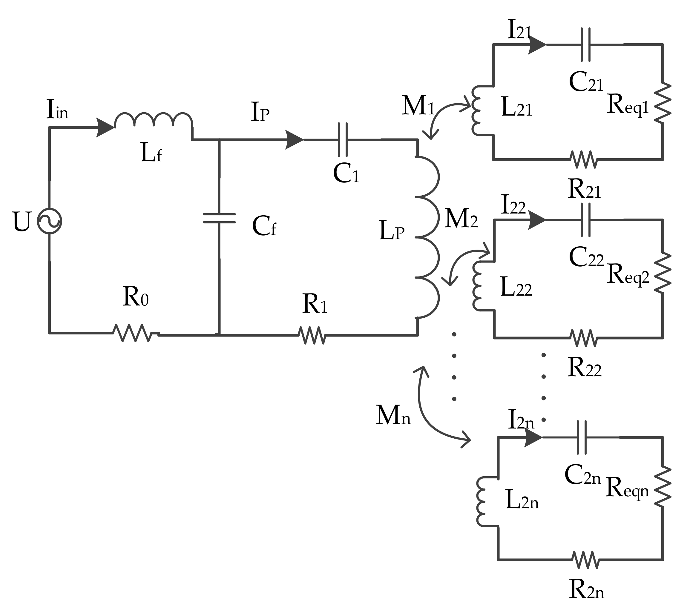
Since the development of wireless power supply technology, there are four basic resonance compensation networks and compound resonance compensation networks such as LCC-S. The most commonly used of the four basic compensation networks is the series-series (SS) structure. It is easy to realize matching capacitance in the SS structure. However, in a multiload system, if the transmitter adopts a series compensation structure, the track current cannot achieve a constant current. The LCC structure can achieve constant current output at the transmitter without considering the internal resistance of the coil, and does not need to add a control device. Therefore, this paper adopts the LCC-S type compensation network, and the equivalent circuit model of the system is shown in Figure 2. Among them, Lf, Cf and C1 are the compensation inductance and compensation capacitance of the LCC compensation network at the transmitter. Lp, L2i (i = 1, 2, ...) are the self-inductance of the track and the receiving coil. C2i (i = 1, 2, ...) is the series compensation capacitance of each receiving coil. U is a high-frequency AC power source, which is converted from a DC power source through an inverter. Mi is the mutual inductance between each receiving coil and the track. R0, R1, R2i are the self-resistance of Lf, Lp and L2i, respectively. Reqi is the equivalent resistance of the load.
In Figure 2, the impedance of each load receiving end can be expressed as:
In order to enable the system to transmit more energy and work in a high-efficiency section, the working frequency of each secondary side should be the same as that of the primary side system—that is, the working frequency of the system should meet the following formula:
At this time, the reflected impedance of the primary side system is the sum of the reflected impedance of each secondary side:
Therefore, the input impedance of the primary side can be expressed as:
From Kirchhoff’s voltage equation, the track current and the output voltage at the load are:
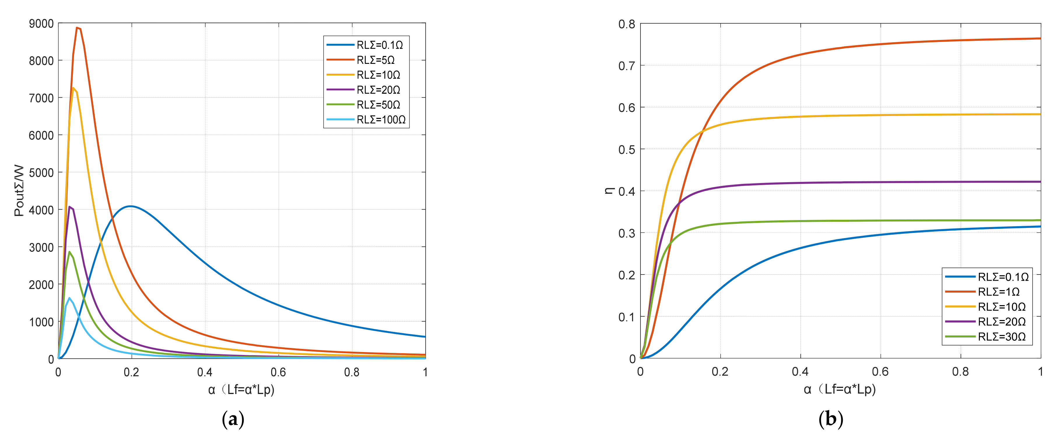
It can be seen from Equations (5) and (6) that when the input voltage of the system is constant, the track current and the output voltage of each load are related to the series compensation inductance Lf, the mutual inductance of the load and its equivalent impedance. We will analyze the impact of the load in the Section 3. This part only analyzes the value of the series compensation inductor. For the value analysis of the series inductance Lf, we will start with the transmission power PoutΣ and efficiency η. First, let Lf = α × Lp (0 < α < 1), then the total output power of the multiload system is (assume that the coupling coefficient ki between each receiving coil and the transmitting track is the same and the maximum value kmax):
Let , the total output and transmission efficiency of the system can be simplified as:
From Equations (8) and (9), plot the output power and efficiency curves with α in MATLAB, as shown in Figure 3a,b. It can be seen from the Figure 3a that with the increase in the load resistance, the maximum value of the output power is taken to be around α = 0.05. When RLΣ = 0.1 Ω, the maximum value of PoutΣ is around α = 0.1, so in terms of output power, the smaller the value of α, the better. However, Figure 3b shows that when α < 0.2, the efficiency is low regardless of the value of RLΣ. It is worth mentioning that when the value of RLΣ is very small, the efficiency is also very low, as shown in the blue curve in Figure 3b. In summary, in order to improve the transmission efficiency of the system and meet the transmission power, αa should be taken as around 0.2—that is, Lf should be taken as around 0.2 × LP.
3. Multiload Dynamic Change Process and Transmission Characteristics Analysis
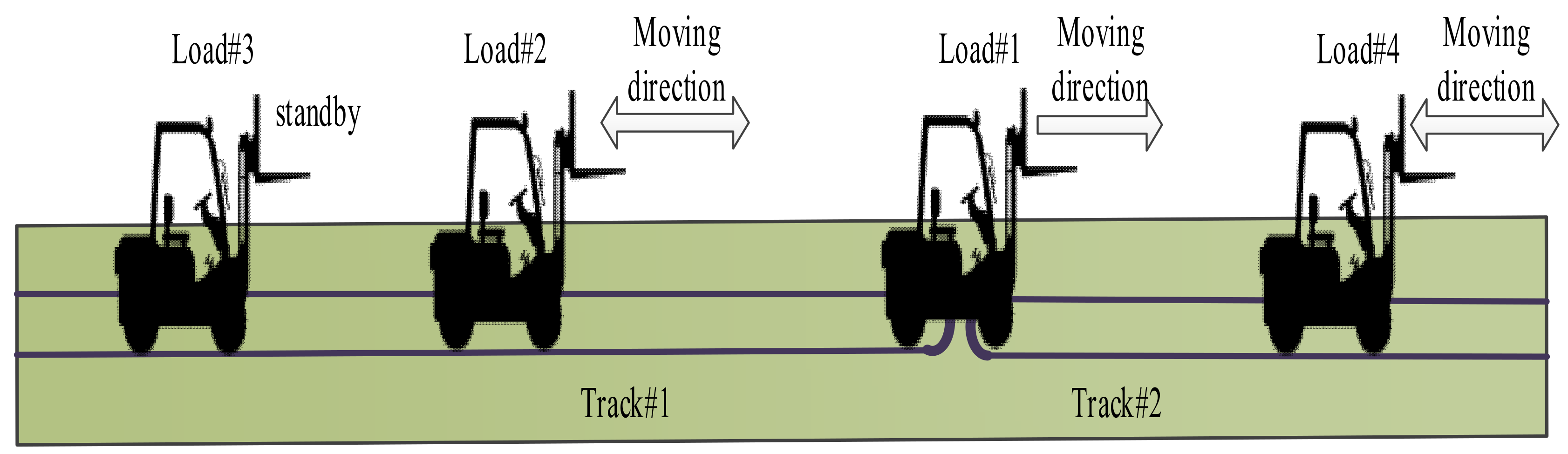
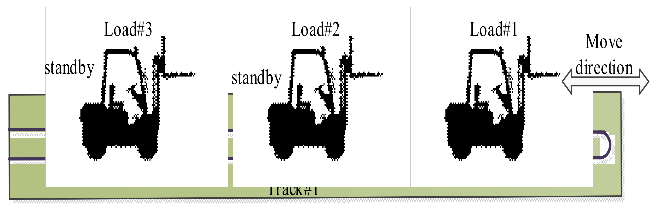
A complex multiload power supply system often contains a dozen or more loads. This paper only analyzes a simple multiload system composed of four loads, as shown in Figure 4. In the figure, it is assumed that both load #2 and load #3 are running on track #1, load #4 is running on track #2, and load #1 is switched from track #1 to track #2. Therefore, the load can be divided into two types based on the different tracks of the load: (1) loads running on the same track; (2) loads running on two tracks—that is, loads that switch from one track to another. The following is a simulation analysis of the system under these two motion states.
3.1. The Influence of Mutual Inductance Changes on the System
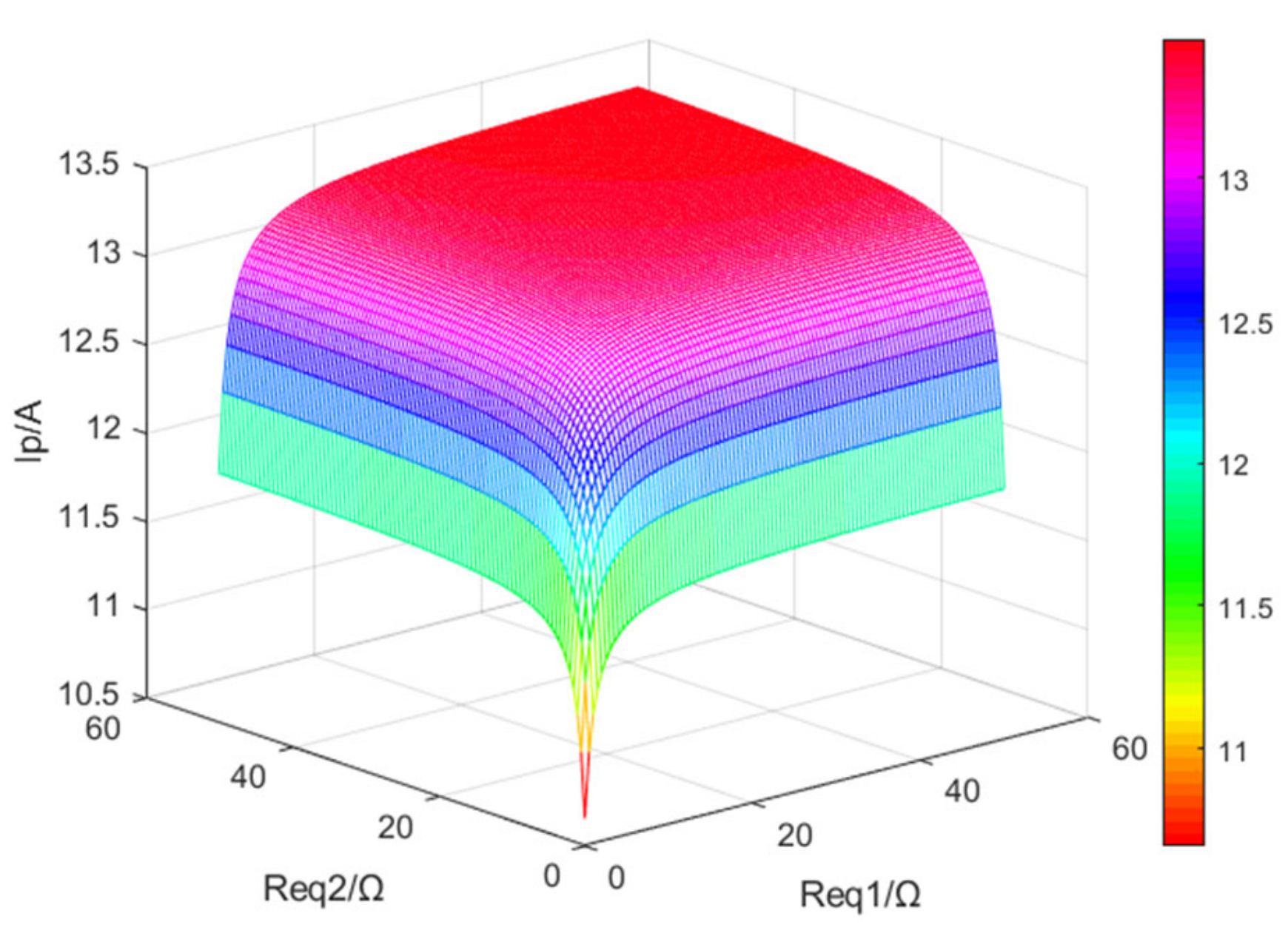
During the movement of the load, the position between the receiving coil and the transmitting track changes constantly—that is, the mutual inductance changes within a certain range. We know that when the distance between the receiving coils is far enough, there is no coupling between the receiving coils. When the receiving coil of any one of the loads shifts laterally, the mutual inductance of the other loads is not affected by it. The current of track #1 in Figure 4 is simulated and calculated, and the change surface diagram of the coupling coefficients k1 and k2 of load #1 and load #2 and the track current is obtained, as shown in Figure 5.
In Figure 5, as the coupling coefficients of the two loads change, the maximum value of IP is 13.5 A and the minimum value is 12.4 A. The difference in current changes is small, so we can consider that the track current is constant and not affected by mutual inductance. Therefore, it can be considered that when any load in the system shifts laterally, it will not affect the operation of other loads in the system.
It can be seen from Equation (6) that the output voltage of the load is mainly related to the rail current Ip, the mutual inductance M and the equivalent load Req. Therefore, as mentioned above, when the receiving coil of each load is offset and the mutual inductance M changes, it has almost no effect on the track current. Therefore, when Ip and Req remain unchanged, the output voltage UL of the load is mainly affected by the mutual inductance M.
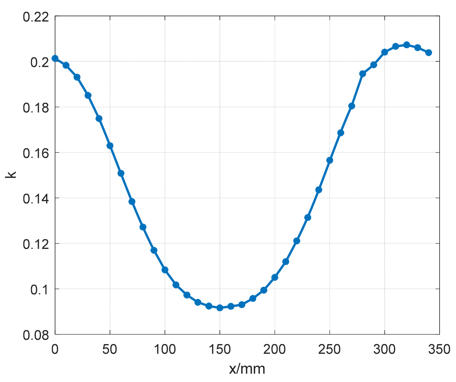
Due to the long power supply distance, the track is mostly composed of several shorter single-coil tracks, and there is a gap between every two tracks. Therefore, when the load is switched from one track to the adjacent track, its receiving coil will be coupled to the two tracks at the same time, as shown in Figure 6. By establishing a 3D simulation model as shown in Figure 6, the coupling coefficient k between the receiving coil and the two tracks is obtained, and the graph shown in Figure 7 is drawn. The abscissa X in Figure 7 represents the distance between the secondary coil AB and track #1. We can see that the coupling coefficient k first decreases and then increases during the switching process, with a minimum value of 0.092. Therefore, in the case of no lateral shift, the output voltage of the secondary side will first decrease and then increase until the receiving coils all move to track #2.
3.2. The Influence of Load Resistance on the System
This paper first takes the dual load system as an example to analyze the impact of load resistance on the system. Figure 8 is a curved surface diagram of the current of the track varying with the resistance of the two loads. It can be seen that the track current tends to be stable as the resistance increases, and the maximum difference is 2 A, so it can be considered that the track current is basically not affected by the load resistance. The analysis in Section 3.1 shows that the track current can remain unchanged when the mutual inductance and resistance change. Therefore, we believe that the primary side system with LCC as the compensation network can provide a relatively stable electromagnetic environment for the load.
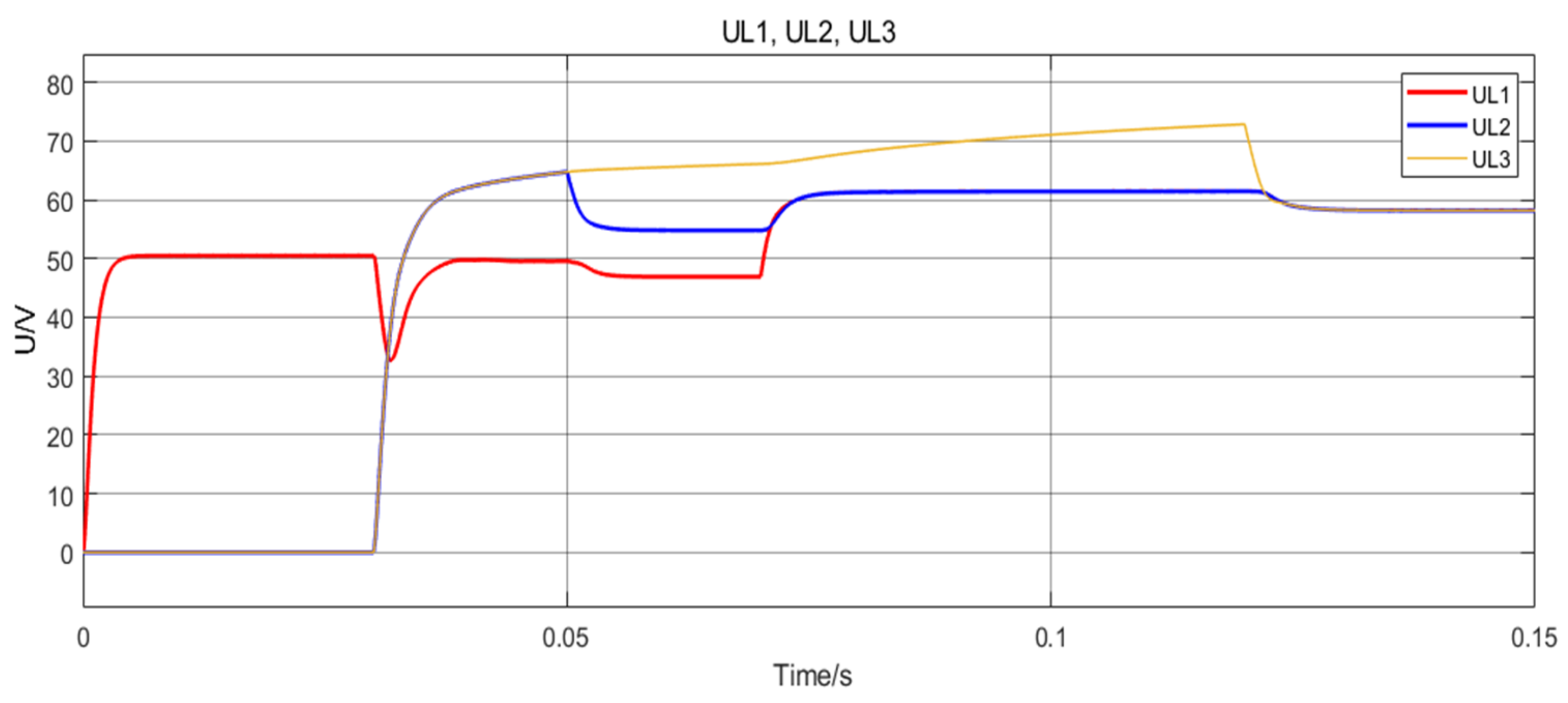
First, the simulation models of the dual-load system and the three-load system were established in Simulink to observe the changes of other loads in the system and its own output characteristics when the load changes. Figure 9 is an analysis diagram of the motion states of three loads on the same track, where load #2 and load #3 are in a state to be started, and load #1 is in a motion state. The output voltage waveforms shown in Figure 10 and Figure 11 are obtained through simulation.
The waveform shown in Figure 10 shows that in the dual-load system. Load #1 is always in operation, and its resistance Req1 increases from 3 Ω to 10 Ω at 0.07 s. Load #2 starts at t = 0.03 s, and its resistance increases from 3 Ω to 10 Ω at 0.09 s. It can be seen from Figure 10 that when load #2 starts, the output voltage UL1 of load #1 fluctuates suddenly and then returns to 50 V, but when Req1 increases, UL1 increases significantly, and the output voltage UL2 of load #2 also increases. At t = 0.09 s, as Req2 increases, UL1 and UL2 both decrease. Therefore, it can be seen from the waveform diagram that in a dual-load system, a change in one load will not only change its own output voltage, but also affect the output voltage of other loads.
It can also be seen from the simulation results of the three-load system (as shown in Figure 11) that when load #2 and load #3 start at t = 0.03 s, the output voltage UL1 of load #1 suddenly drops and gradually recovers but its value drops slightly. However, compared with the waveform in Figure 10, the value of UL1 in Figure 11 has a larger drop. Therefore, it can be speculated that when multiple loads (more than two) are started at the same time, the running load will have greater fluctuations, which will affect the stability of its power supply.
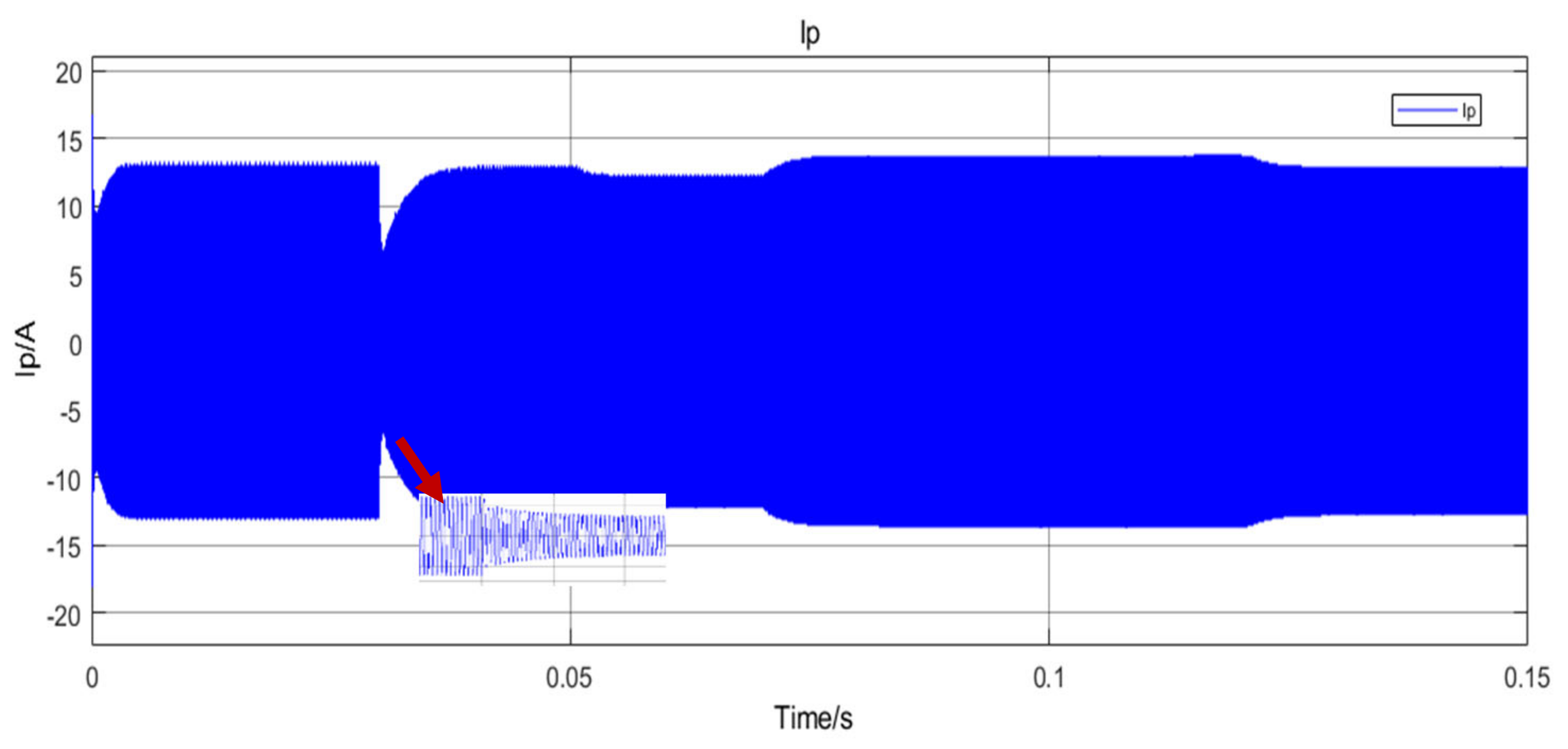
Through the simulation analysis of Section 2 and Section 3, it can be concluded that in a multiload system, the stable operation of the load is not only affected by the change of its own load resistance and the change of mutual inductance, but also by the operating status of the other loads in the same system. That is, the operation between each load is not independent. The reason for this independency is that changes in load will affect the changes in track current (as shown in Figure 12), which in turn will affect all loads on the same track. Therefore, it is necessary to adopt constant voltage control in a multiload system with a constant voltage output.
4. Multi-Load Wireless Power Supply System Based on Secondary Side Control
From the above dynamic process analysis, the output voltage of each load is not only related to the change of its own load resistance, but also related to the change of other loads on the same track. During the movement, in order to ensure the stability of the load output voltage, it is usually necessary to add a control circuit in the wireless power supply system.
The common voltage stabilization control strategies are the primary side control, secondary side control and overall control. The primary side control is mainly used to make the track current constant by changing the input voltage, but this method cannot make the output voltage of the load constant when the mutual inductance of the load changes. At this time, a secondary side control needs to be added to form an overall control.
From the above analysis, the independence of each load on the secondary side is affected by the track current; so as long as the track current does not change, the load independency can be eliminated. However, it can be seen from Figure 12 that when the load starts, the track current Ip will drop, causing UL1 to fluctuate downward, but from a general point of view, the increase or decrease in the track current Ip is small when the load resistance changes. Therefore, this paper ignores the track current changes when designing the control circuit, and only considers adding a control circuit on the load side. A Buck converter is added after each rectifier circuit to achieve the purpose of constant voltage output by adjusting the duty cycle of the switch. The structure diagram of the secondary side circuit based on the Buck converter is shown in Figure 13. The uncontrollable rectifier is connected to the load through the Buck converter.
There are many ways to control the Buck changer. In [17], the PID and sliding mode control methods are used, respectively, and the two methods are compared. In the Simulink simulation, the response speed of the PID algorithm is 0.005 s, while the sliding mode control is only 0.001 s, so this papaer adopts the PWM sliding mode control method to realize the control to Buck converter.
In the process of wireless power supply, changes in load and mutual inductance will change the output voltage. In order to make the output voltage constant, the control strategy shown in Figure 13 is designed. First set the load constant output voltage ULre, and detect the actual output voltage UL of the load, Then calculate the error x1 between the output voltage and the reference voltage, that is, x1= ULre − UL. At the same time, the error rate and integral are sent to PWMSMC together to calculate and adjust the output PWM duty cycle. The design process of PWMSMC is as follows:
Define the error variable x1 of the output voltage:
Output voltage error rate of change x2 and its integral x3:
According to the working state of the switch tube SW, the working of the Buck circuit can be divided into two modes. When u = 1, SW is turned on and D is turned off, and the power supply charges the inductor L, the capacitor C and the load Req. At this time, the inductor current iL increases. When u = 0, SW turns off and D turns on, inductor L and capacitor C discharge to load Req, and iL decreases [18]. It can be seen that the circuit works in current continuous mode (CCM), and its state space equation is as follows:
To ensure the existence of the sliding mode state of the Buck converter, should be satisfied, where S is the sliding mode surface function—that is, α1, α2, and α3 are the sliding coefficients.
(1) , at this time the switching function u = 1.
(2) , at this time the switching function u = 0.
Synthesize Equations (14) and (15) to obtain simplified existence conditions:
Among them , , . Finally, the equivalent control function Equation (16) is transformed into the duty cycle d. Among them , the following relationship between the control signal and the ramp signal is obtained. This formula can be used in the actual realization of PWMSMC, which is:
And .
To prove the stability of the above sliding mode control, the Lyapunov function is constructed as follows:
Derivation of Equation (18) to obtain the following equation:
From the above process, , and , so . According to the Lyapunov stability theory, the controller is progressively stable.
In order to verify the performance of the controller, a simulation model was built in Simulink to simulate the change of load Req. The parameters of the wireless power supply system are shown in Table 1.
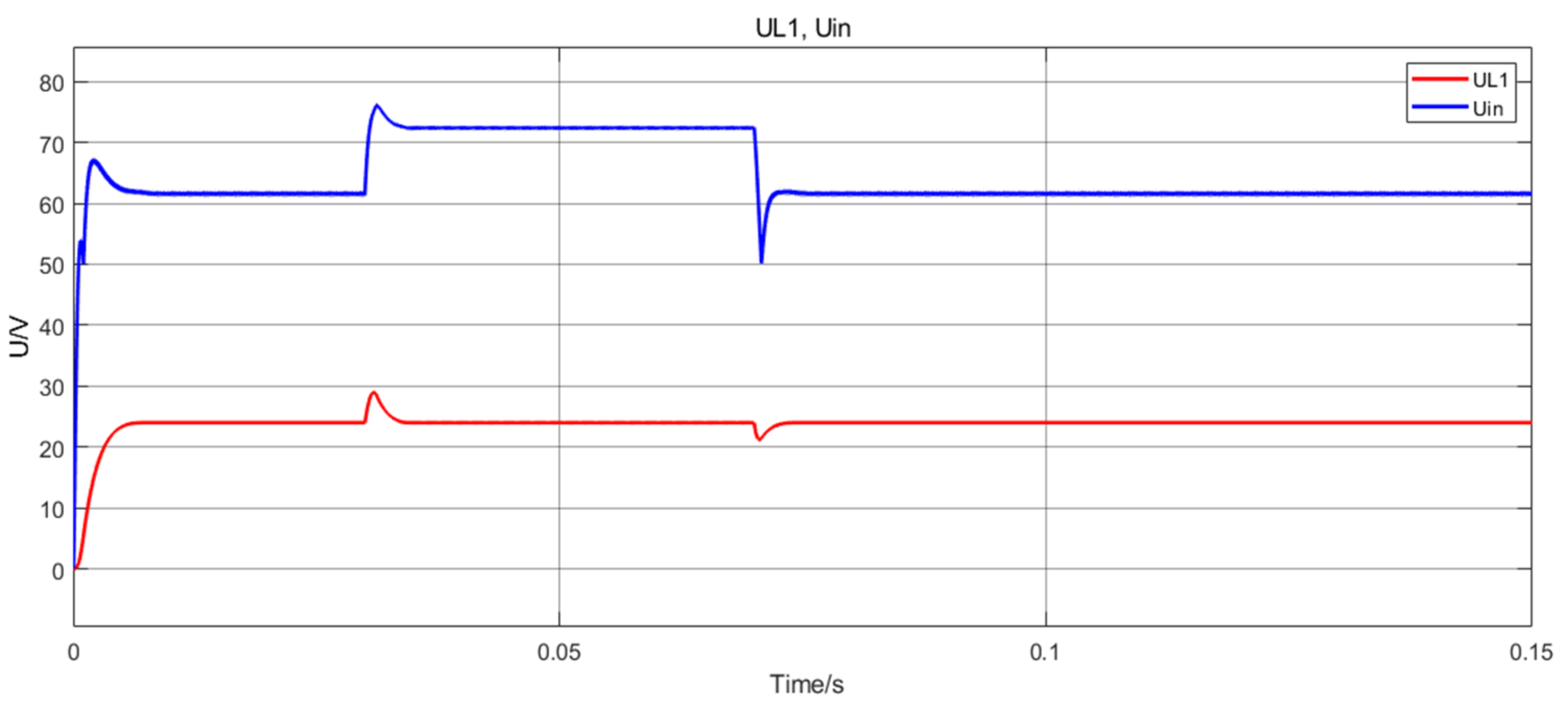
According to the constant voltage control strategy, the duty cycle generated by PWMSMC is used to adjust the load output voltage value to the reference output voltage value. Figure 14 is a waveform diagram of the output voltage UL1 of load #1 and the input voltage Uin of the Buck circuit in the single-load system. Figure 15 is a waveform diagram of the output voltage of each load and the input voltage Uin of the Buck circuit in the three-load system. It can be seen from Figure 14 that Uin fluctuates due to the change of the resistance of load #1 at t = 0.03 s and t = 0.07 s. This is because the LCC-S system cannot maintain a constant voltage output due to the internal resistance of the inductor, but judging from the waveform of the output voltage UL1 of load #1, t = 0~0.03 s, the resistance value of load #1 Req1 = 3 Ω, and the output voltage is the set reference voltage value of 24 V. When t = 0.03 s, Req1 changes from 3 Ω to 10 Ω, UL1 fluctuates upward, and returns to 24 V after 4 ms. When t = 0.07 s, Req1 decreases from 10 Ω to 3 Ω, UL1 fluctuates downwards, and stabilizes at 24 V after 2.7 ms. The results show that, in a single-load system, by controlling the change of Buck duty cycle by PWMSMC, a fast dynamic response and stable output voltage waveform can be obtained.
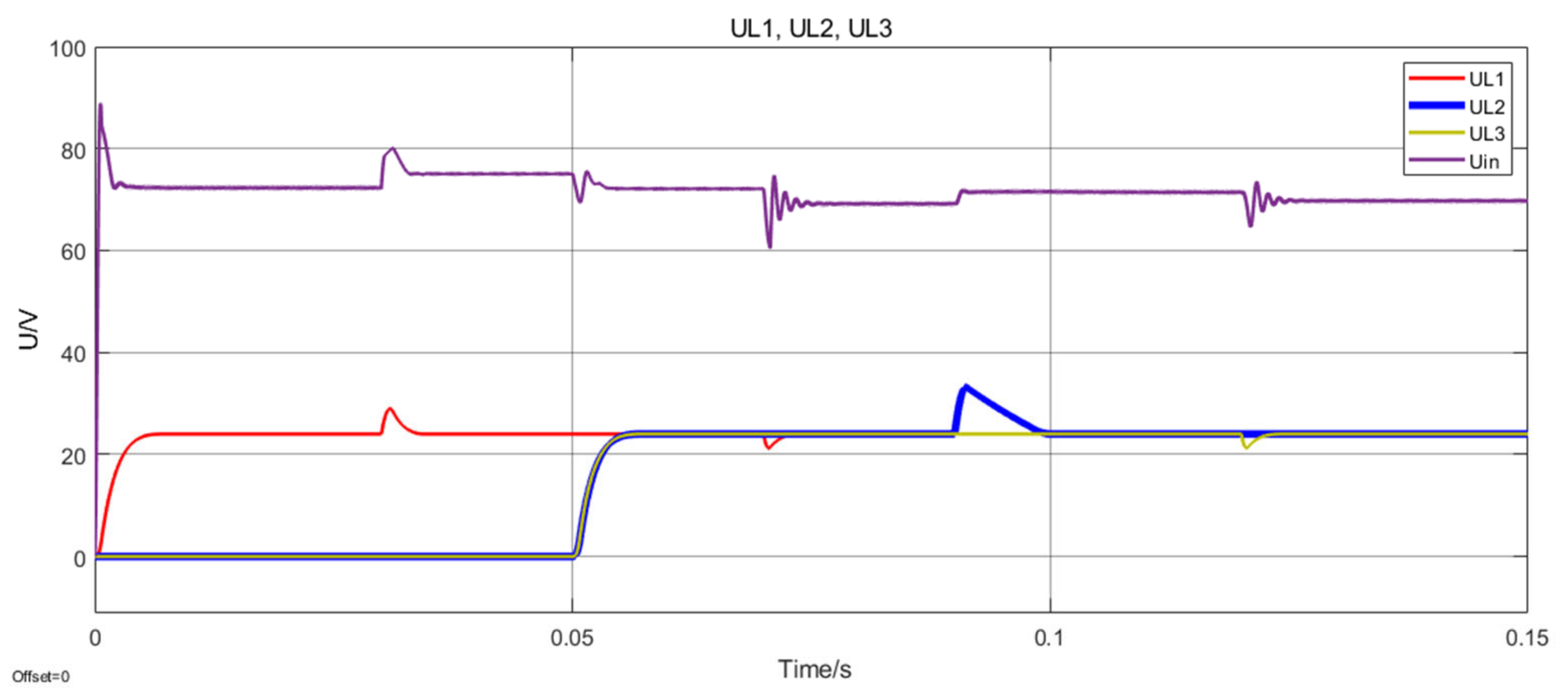
Figure 15 represents a three-load system. When t = 0.05 s, load #2 and load #3 start with Req2 = 3 Ω and Req2 = 10 Ω, respectively. At this time, it can be seen that the output voltage UL1 of the load #1 has not fluctuated and has been maintained at 24 V. At t = 0.09 s, when the resistance of load #2 suddenly increases to 50 Ω, the voltage of load #1 and load #3 does not fluctuate. Therefore, it can be considered that the disturbance between each load has been completely eliminated, which solves the problem of affecting the output of other loads when multiple loads are started at the same time in the system. For load #2, when the resistance value increases greatly, the fluctuation time of UL2 is about 9.8 ms, so the control system has faster instantaneous characteristics and meets the needs of the system’s dynamic stability.
5. Experimental Validation
5.1. Experimental Setup
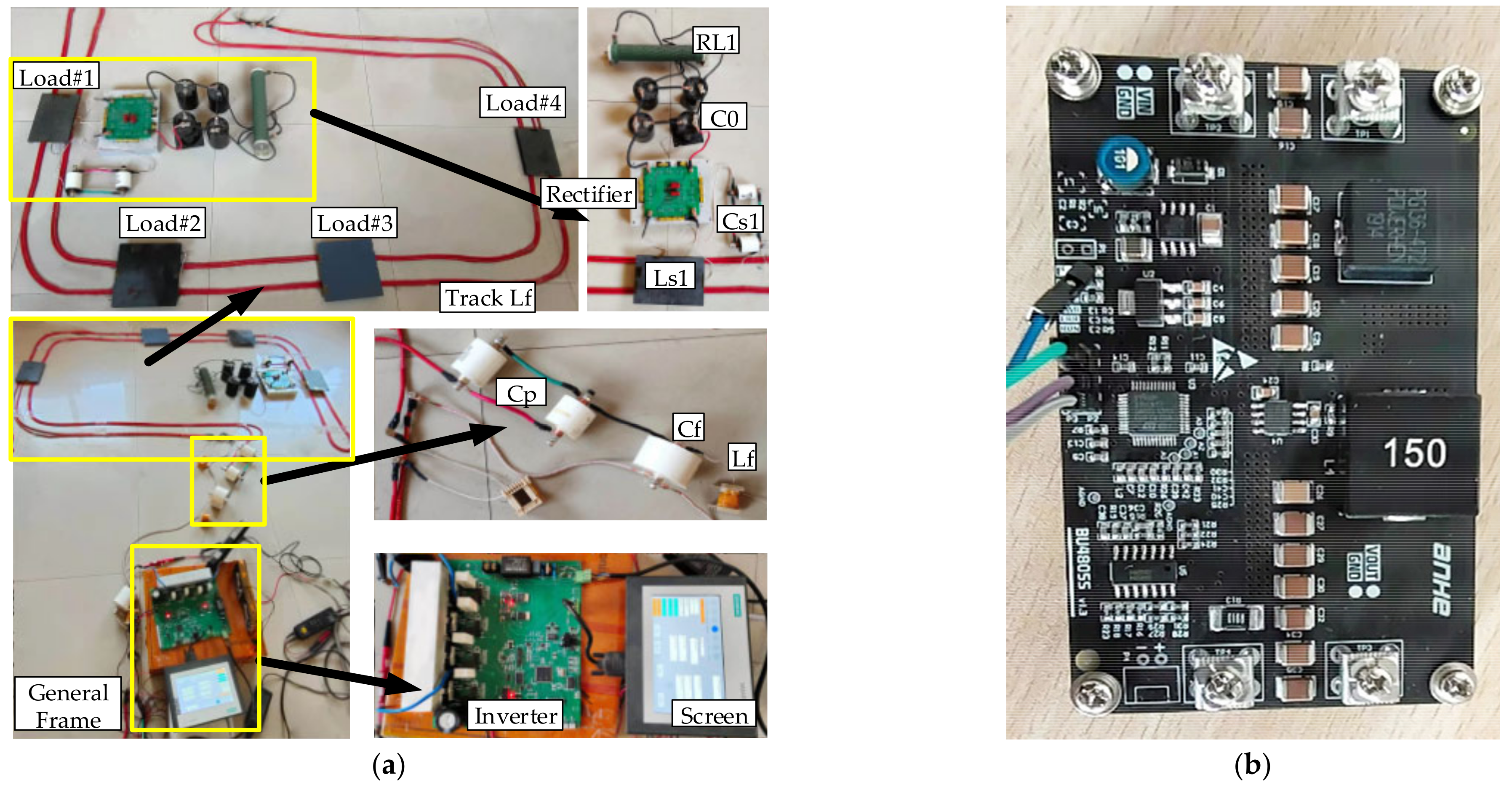
In order to verify the correctness and effectiveness of the above analysis, this paper builds an experimental platform as shown in Figure 16a.The whole experimental platform includes the DC power supply, the inverter, the LCC type compensation network, the track, four receiving coils, the rectifier and the load. The entire experimental platform is built according to the system topology shown in Figure 2, and the parameters are the same as Table 1. Among them, the inverter converts the DC voltage into an AC voltage with a frequency of 80 kHz, which is filtered by the LCC type compensation network and flows into the track. The track and each receiving coil are made of Litz wire with different diameters, and they are 2 turns and 20 turns, respectively. The distance between each receiving coil and the track is 2 cm. Figure 16b shows the DC-DC module added for the control system.
5.2. Results
5.2.1. Experimental Verification of the Value Range of Series Compensation Inductance
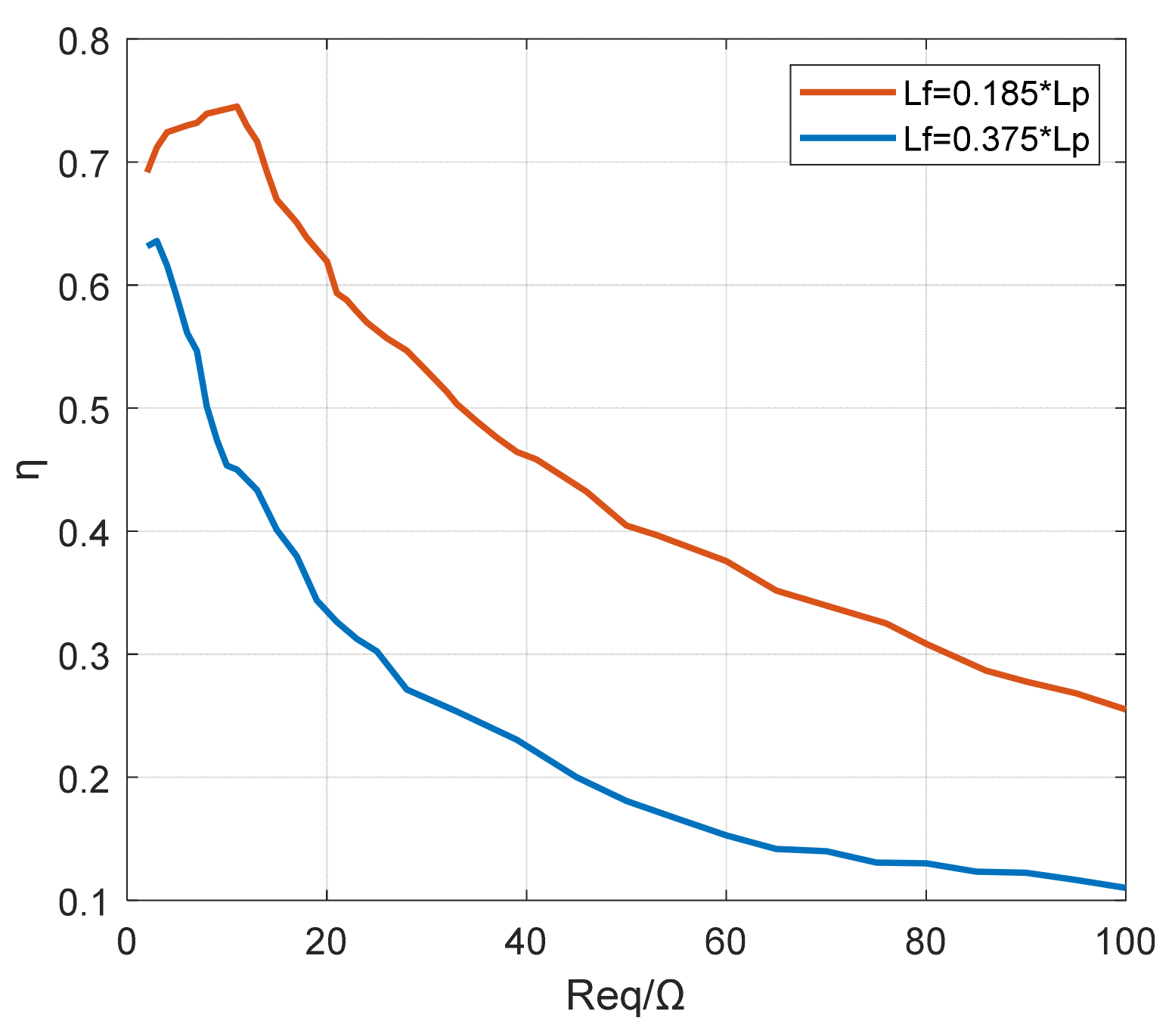
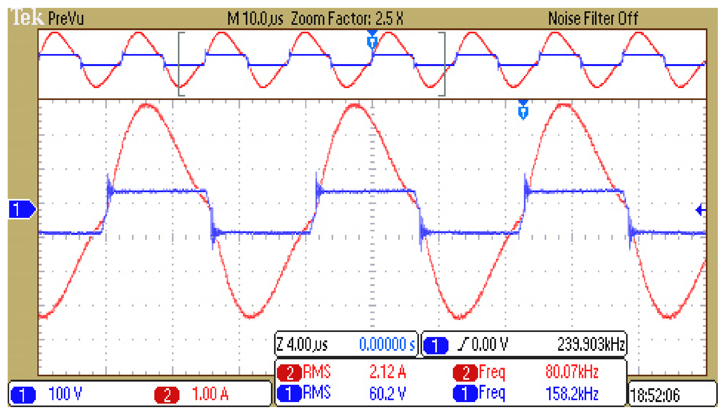
In order to verify the correctness of the value range of the series compensation inductance Lf proposed in Section 2, two Lf coils with different values and the corresponding compensation capacitors are set, respectively. The specific parameters are shown in Table 2. The wireless power supply system under the single load mode is experimentally verified, and the experimental data is plotted into a graph as shown in Figure 17. Figure 18 is a waveform diagram of the output voltage and output current of the inverter device. It can be seen from Figure 17 that when Lf = 7.2 μH, that is, Lf = 0.185 × Lp, the transmission efficiency of the system is significantly higher than that when Lf = 7.2μH (Lf = 0.375 × Lp). This is the same as the conclusion obtained in Section 2, so Lf should be around 0.2 × LP.
5.2.2. Dynamic Experiment of Multiload System
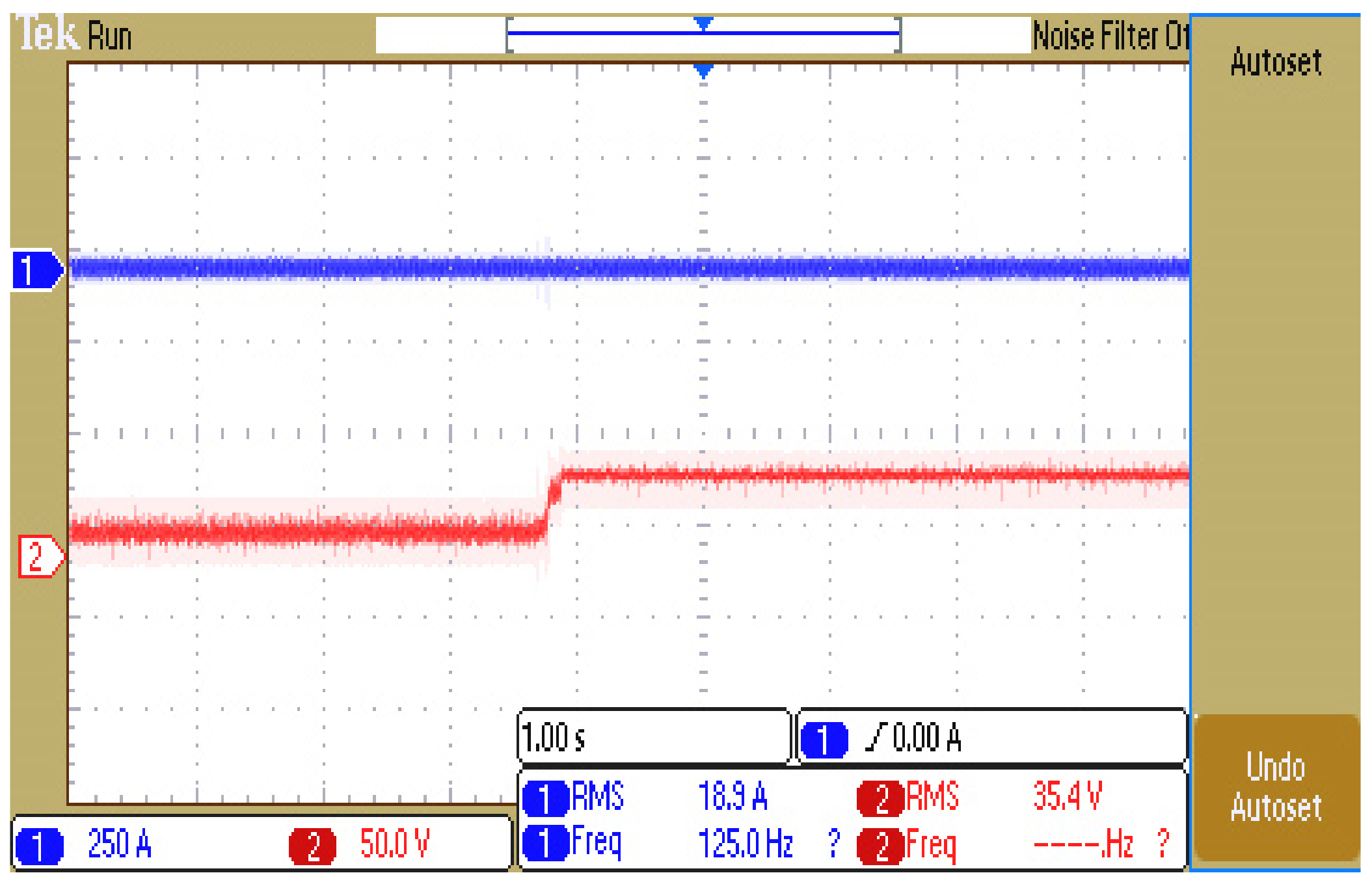
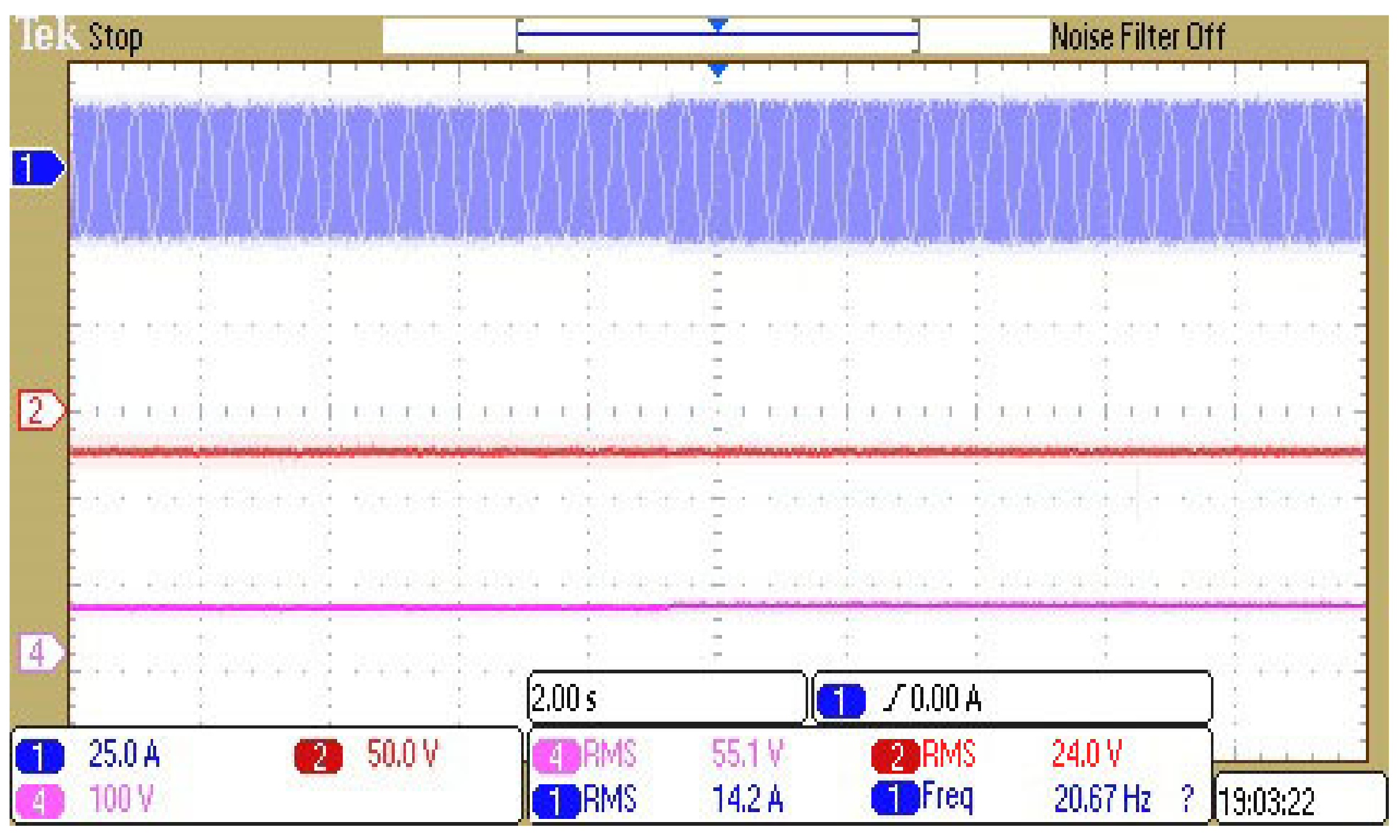
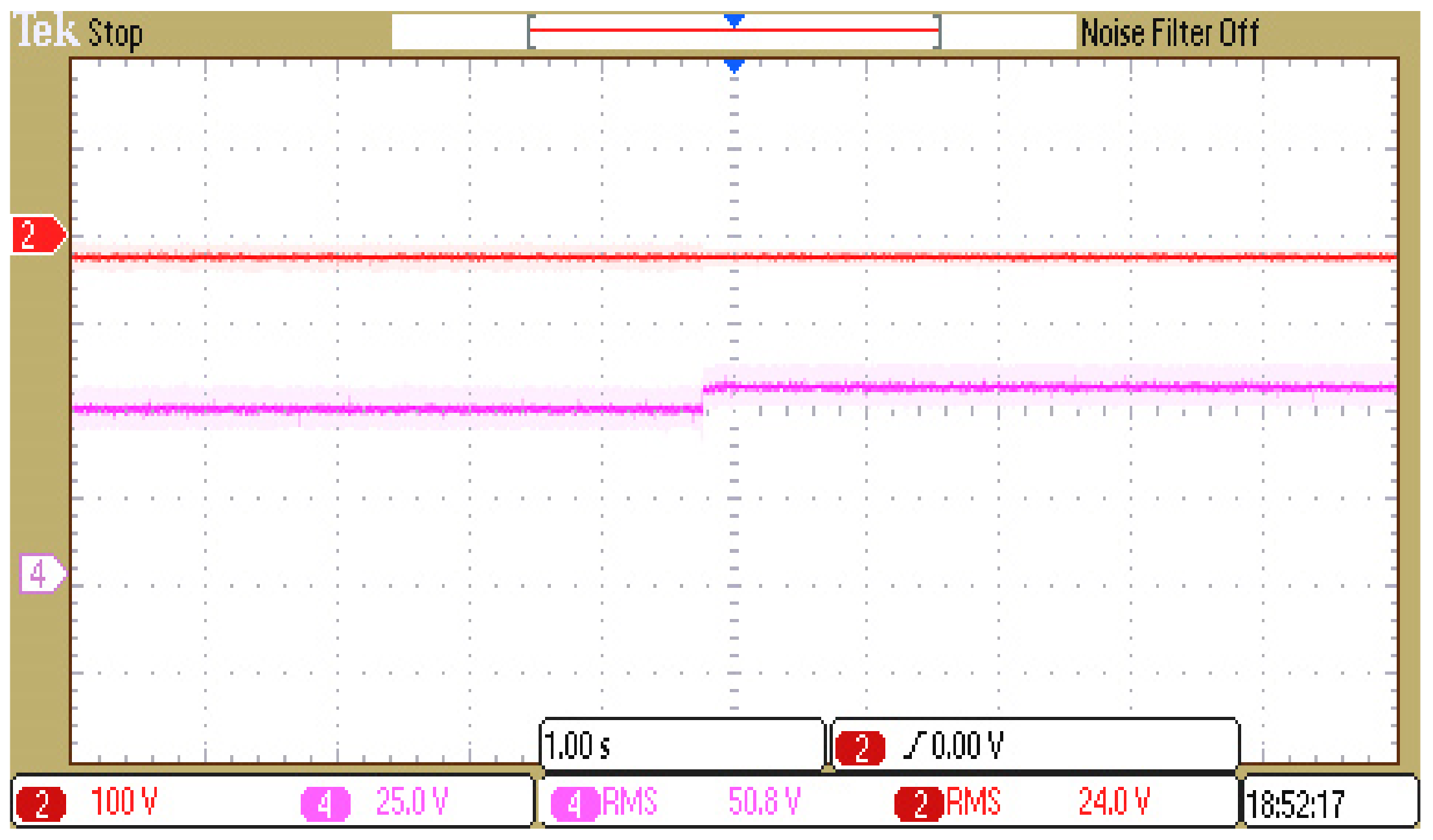
Based on the experimental results in Section 5.2.1, we select the first set of experimental parameters for dynamic testing of the multiload system. In the experiment, first we let load #1 be in a stable power supply state. Then we turn on the switch of load #2 to start the power supply and obtain the waveform shown in Figure 19. Then we turn off the switch of load #2, and start the switches of load #2, load #3, and load #4 at the same time to obtain the waveform diagram shown in Figure 20. It can be seen from Figure 19 and Figure 20 that when a new load is added to the same track, the output voltage of load #1 increases, but the increase is smaller; but when three new loads are added, the output voltage at both ends of load #1 has a significant increase. Therefore, the experiment verifies that the addition or removal of a new load on the same track will affect the output of other loads, and the greater the number of loads added or removed, the greater the impact on it. Then we added the DC-DC and its control module as shown in Figure 16b between the filter capacitor C0 and resistor Req1 of load #1 to verify the practicability of the control method adopted in Section 4. In the experiment, an STM32F334C8 microcontroller is used to realize the sliding mode control of the buck converter and generate the required PWM signal to track the constant voltage output of the system [18]. Use the Tektronix MDO3024 oscilloscope to observe the output current, inverter output voltage and other signals, and obtain the waveform diagram shown in Figure 21 and Figure 22. Among them, curve 1 represents the track current Ip, curve 2 represents the output voltage UL1 of load #1, and curve 4 represents the input voltage of the DC–DC module in load #1. We set the reference voltage as ULre = 24 V in the experiment. As can be seen from the figure, no matter how the other loads change, UL1 can still maintain 24 V unchanged. Therefore, it shows us that the control method has a certain practicability and improves the mutual independence between loads.
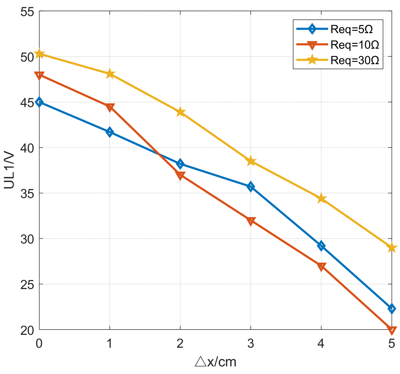
In order to verify the change of the output voltage when the receiving end of the load is shifted, this paper does the following coil shift experiment. First, when the Buck circuit is not added, move the receiving coil of load #1 to obtain the graph shown in Figure 23. In Figure 23, the input DC voltage is 98 V, the abscissa Δx represents the distance of the lateral offset of the receiving coil, and the ordinate UL represents the output voltage of the load. It can be seen from the curve in the figure that when the receiving coil shifts laterally, its output voltage gradually decreases as the shift distance increases. In the figure, when Req = 5 Ω, its maximum output power reaches 405 W.
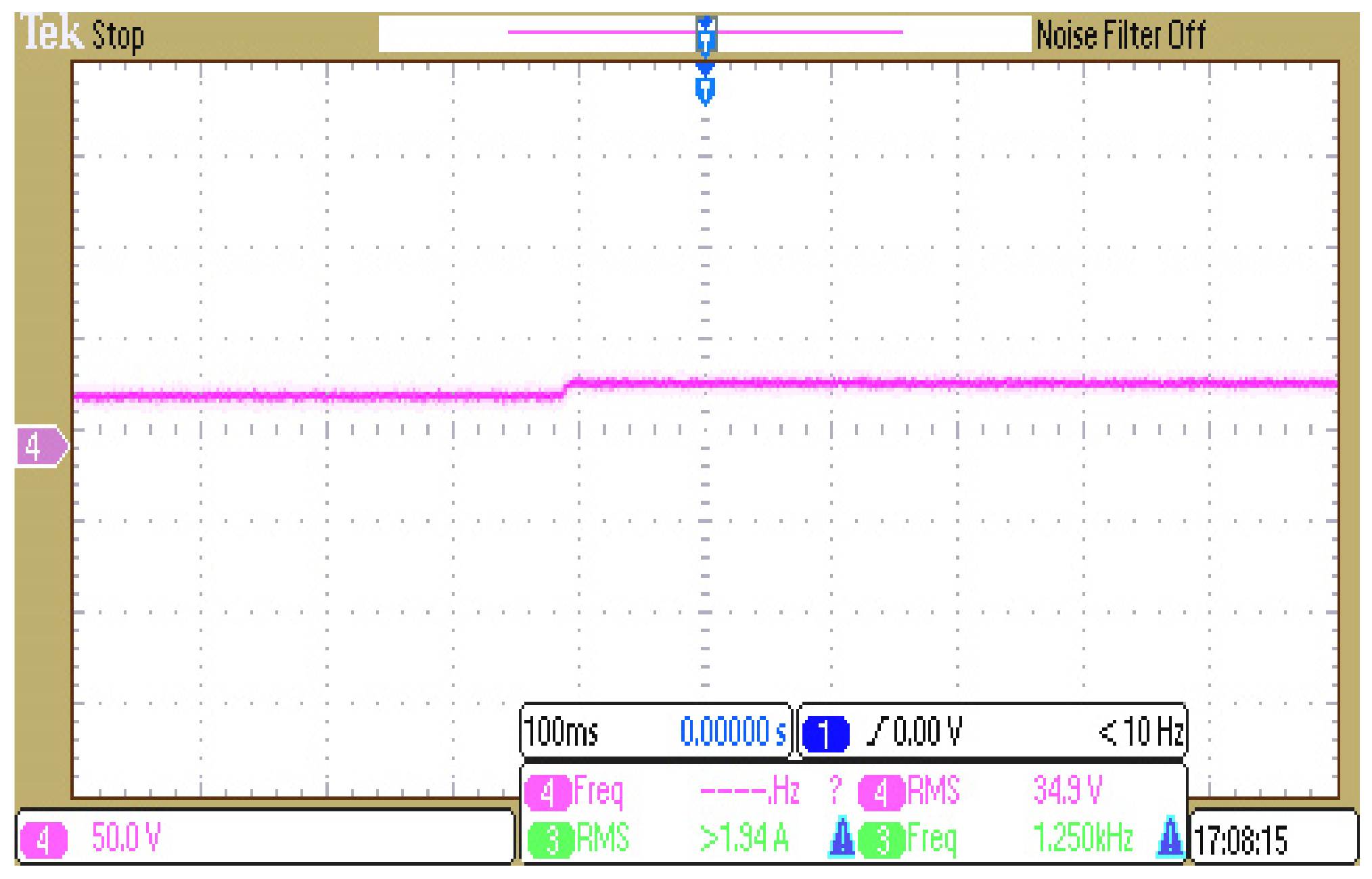
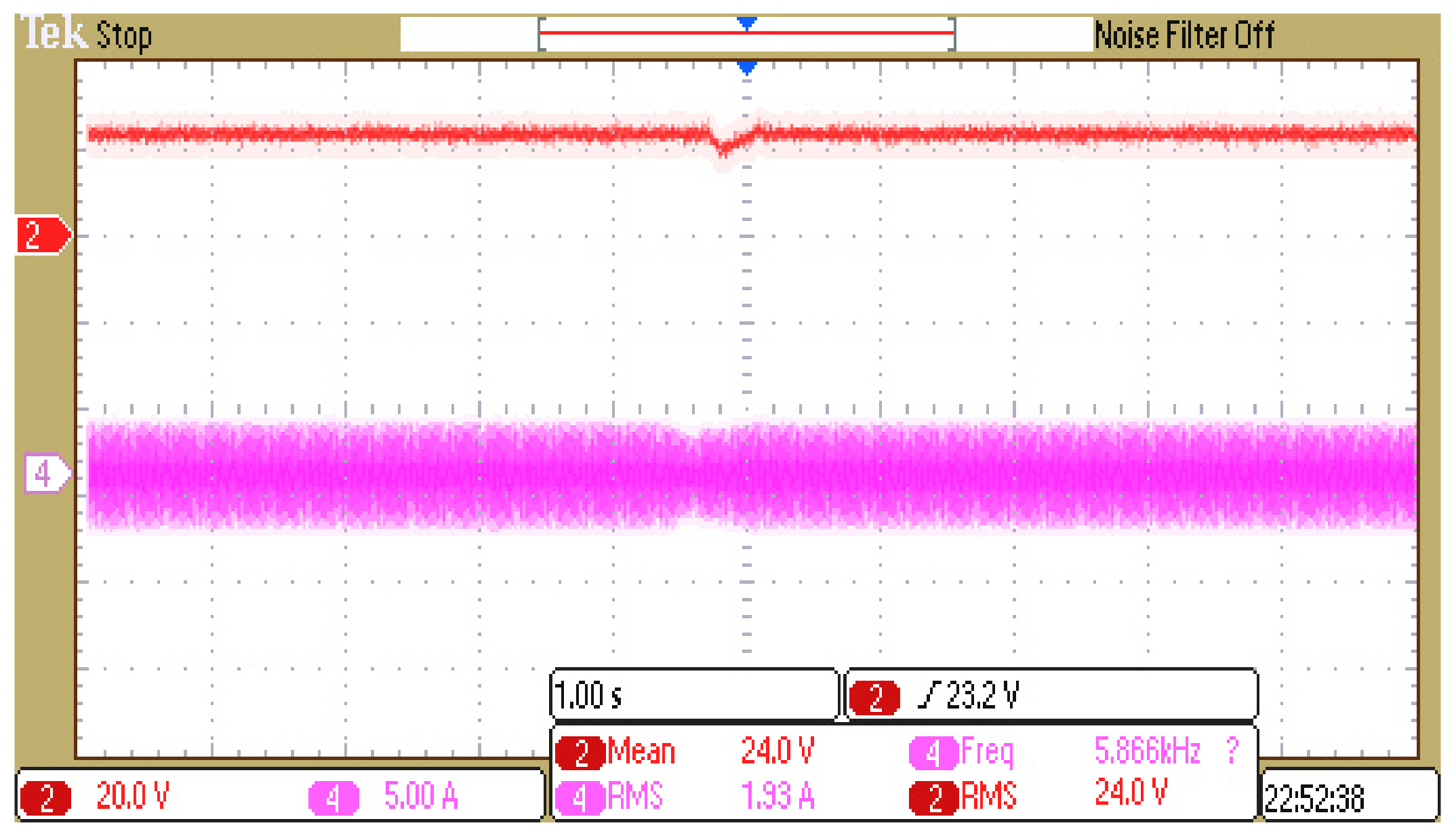
When the Buck circuit is added to the receiving end of load #1, the receiving coil is offset by 2 cm from the positive alignment position, and the waveform shown in Figure 24 is obtained. It can be seen from the figure that the red curve first shifts downwards and then gradually returns to 24 V. Therefore, the experiment proves that the control system used in this article can achieve a constant voltage output within a certain offset range.
Through the above simulation and experimental verification, this article uses the secondary side control method for each load to realize the constant voltage output of the load. Compared with methods such as overall control, the number of devices added by the system is significantly reduced, and it is convenient to change the parameters of the load side, so it is more suitable for practical applications.
6. Conclusions
This paper analyzes the dynamic process of multiload induction wireless power supply system and its control strategy for stable output. First of all, this paper establishes a multiload equivalent circuit model based on the LCC-S resonance compensation network, and derives the expression of the output voltage of each load. The analysis shows that when the self-resistance of the inductor is not negligible, the output voltage is not only related to the change of its own load resistance, but also related to the number of power loads on the same track. Then, the simulation models of dual-load and triple-load systems were established in Simulink. It analyzes the change of the output voltage of load #1 after load #2 is started in the dual-load system and the change characteristics of the corresponding output voltage when the resistance of the two loads changes. It can be concluded that when multiple loads are activated at the same time, it will have a greater impact on the load in motion on the track. Therefore, there is a connection between loads, that is, they will change as other loads change. In order to make the loads independent of each other and meet the requirements of the output voltage of each load, this article adopts the control strategy of secondary side control. By controlling the duty cycle of the Buck converter, the positive output voltage is stable. The correctness and rapidity of the control strategy are verified by simulation. Finally, the correctness of the series compensation inductance range and the practicability of using PWMSMC to achieve voltage stability are verified through experiments.
Author Contributions
Conceptualization, S.F. and Z.L.; formal analysis, S.F.; funding acquisition, Z.L.; investigation, Z.L. and G.F.; methodology, S.F. and G.F.; project administration, Z.L. and Y.H.; resources, Z.L. and Y.H.; software, S.F., N.A. and Y.H.; supervision, Z.L.; validation, S.F., G.F. and N.A.; writing—original draft, S.F.; writing—review and editing, S.F. All authors have read and agreed to the published version of the manuscript.
Funding
This research was funded by the Science and Technology Research Project of Shandong Province under Grant No. 2019GGX104080.
Conflicts of Interest
The authors declare no conflict of interest.
References
- Wesemann, D.; Witte, S.; Michels, J. Effects of multiple loads in a contactless, inductively coupled linear power transfer system. In Proceedings of the 2009 International Conference on Electrical and Electronics Engineering—ELECO 2009, Bursa, Turkey, 5–8 November 2009; pp. I-54–I-59. [Google Scholar]
- Su, H.; Zhou, Z.; Liu, Z. Research review and prospect of intelligent dynamic wireless charging system for electric vehicles. Chin. J. Intell. Sci. Technol. 2020, 2, 1–9. [Google Scholar]
- Zhang, Q.; Huang, Y.; Niu, T.; Xu, C. Dynamic Wireless Charging Power Control of Electric Vehicle Based on Neural Network. Automob. Technol. 2017, 1–5. [Google Scholar]
- Xu, Y.X.; Boys, J.T.; Covic, G.A. Modeling and controller design of ICPT pick-ups. In Proceedings of the International Conference on Power System Technology, Kunming, China, 13–17 October 2002; Volume 3, pp. 1602–1606. [Google Scholar]
- Covic, G.A.; Elliott, G.; Stielau, O.H.; Green, R.M.; Boys, J.T. The design of a contact-less energy transfer system for a people mover system. In Proceedings of the PowerCon 2000. 2000 International Conference on Power System Technology, (Cat. No.00EX409), Perth, Australia, 4–7 December 2000; Volume 1, pp. 79–84. [Google Scholar]
- Boys, J.T.; Elliott, G.A.J.; Covic, G.A. An Appropriate Magnetic Coupling Co-Efficient for the Design and Comparison of ICPT Pickups. IEEE Trans. Power Electron. 2007, 22, 333–335. [Google Scholar] [CrossRef]
- Chen, L.; Nagendra, G.R.; Boys, J.T.; Covic, G.A. Double-Coupled Systems for IPT Roadway Applications. IEEE J. Emerg. Sel. Top. Power Electron. 2015, 3, 37–49. [Google Scholar] [CrossRef]
- Choi, S.Y.; Gu, B.W.; Jeong, S.Y.; Rim, C.T. Advances in Wireless Power Transfer Systems for Roadway-Powered Electric Vehicles. IEEE J. Emerg. Sel. Top. Power Electron. 2015, 3, 18–36. [Google Scholar] [CrossRef]
- Xia, C.; Zhao, S.; Yang, Y. Research review on electric vehicle wireless charging system. Guangdong Electr. Power 2018, 31, 3–14. [Google Scholar]
- Choi, S.Y.; Rim, C.T. Recent progress in developments of on-line electric vehicles. In Proceedings of the 2015 6th International Conference on Power Electronics Systems and Applications (PESA), Hong Kong, China, 15–17 December 2015; pp. 1–8. [Google Scholar]
- Kim, J.H.; Lee, B.S.; Lee, J.H.; Lee, S.H.; Park, C.B.; Jung, S.M.; Lee, S.G.; Yi, K.P.; Baek, J. Development of 1-MW Inductive Power Transfer System for a High-Speed Train. IEEE Trans. Ind. Electron. 2015, 62, 6242–6250. [Google Scholar] [CrossRef]
- Lee, S.; Lee, B.; Lee, J. A New Design Methodology for a 300-kW, Low Flux Density, Large Air Gap, Online Wireless Power Transfer System. IEEE Trans. Ind. Appl. 2016, 52, 4234–4242. [Google Scholar] [CrossRef]
- Swain, A.K.; Devarakonda, S.; Madawala, U.K. Modelling of multi-pick-up bi-directional Inductive Power Transfer systems. In Proceedings of the 2012 IEEE Third International Conference on Sustainable Energy Technologies (ICSET), Kathmandu, Nepal, 24–27 September 2012; pp. 30–35. [Google Scholar]
- Beppu, A.; Katsura, S. Realization of transmitter for wireless power transfer to multi loads. In Proceedings of the 2018 IEEE International Conference on Industrial Technology (ICIT), Lyon, France, 20–22 February 2018; pp. 1801–1806. [Google Scholar]
- Yang, L.; Jiantao, Z.; Kai, S.; Guo, W.; Chunbo, Z.; Chan, C.C. Stability Analysis of Multi-load Inductively Coupled Power Transfer System. Trans. China Electrotech. Soc. 2015, 30, 187–192. [Google Scholar]
- Wang, H.; Tang, C.; Zuo, Z.; Wu, X.; Xu, W. Multi-load mode analysis of wireless supplying system for electric vehicles. Electr. Technol. 2019, 20, 6–10. [Google Scholar]
- Ali, N.; Liu, Z.; Hou, Y.; Armghan, H.; Wei, X.; Armghan, A. LCC-S Based Discrete Fast Terminal Sliding Mode Controller for Efficient Charging through Wireless Power Transfer. Energies 2020, 13, 1370. [Google Scholar] [CrossRef] [Green Version]
- Wang, S.-B.; Zhou, Y.-F.; Chen, J.-N. Sliding- mode control and stability analysis in SEPIC converter. Electr. Meas. Instrum. 2007, 10–13. [Google Scholar]
Figure 1.
A typical wireless power transfer system.

Figure 2.
Equivalent circuit model of multiload inductive coupled power transfer (ICPT) system.

Figure 3.
(a) The output power varies with α; (b) the curve of transmission efficiency η changing with α.
Figure 3.
(a) The output power varies with α; (b) the curve of transmission efficiency η changing with α.

Figure 4.
Dynamic analysis diagram.

Figure 5.
Curved surface plot of the track current IP changing with the coupling coefficient of load #1 and load #2.
Figure 5.
Curved surface plot of the track current IP changing with the coupling coefficient of load #1 and load #2.

Figure 6.
Three-dimensional simulation diagram.

Figure 7.
Variation curve of coupling coefficient k.

Figure 8.
Curved surface diagram of the track current with the resistance of two loads.

Figure 9.
Analytical diagram of the motion state of three loads.

Figure 10.
Simulation diagram of output voltage change of load #1 and load #2.

Figure 11.
Simulation diagram of output voltage changes of load #1, load #2 and load #3.

Figure 12.
Waveform diagram of track current Ip.

Figure 13.
Wireless power transfer (WPT) system circuit diagram of the secondary side Buck converter based on LCC-S compensation.
Figure 13.
Wireless power transfer (WPT) system circuit diagram of the secondary side Buck converter based on LCC-S compensation.

Figure 14.
The output voltage of load #1 and the input voltage Uin of Buck circuit.

Figure 15.
The output voltage of each load and the input voltage Uin of Buck circuit.

Figure 16.
(a) Experimental setup. (b) DC–DC module.

Figure 17.
The efficiency curves of the two sets of experiments.

Figure 18.
Inverter output voltage and current.

Figure 19.
The output voltage waveform of load #1 after load #2 starts.

Figure 20.
The output voltage waveform of load #1 after three loads are started at the same time.

Figure 21.
Waveform diagram of output voltage of load #1 and the track current Ip.

Figure 22.
The output voltage waveform of load #1 and the input voltage waveform of DC–DC.

Figure 23.
Output voltage when the receiving coil of load #1 is offset.

Figure 24.
When the receiving coil of load #1 is offset by 2 cm.


Table 1.
Wireless power supply system parameters.
| Symbol | Parameter | Value |
|---|---|---|
| U/V | Input voltage | 60 |
| Lf/μH | Series compensation inductor | 7.2 |
| Cf/nF | Parallel compensation capacitor | 550 |
| C1/nF | Primary side series compensation capacitor | 140 |
| L1/μH | Track coil self-induction | 36.2 |
| R1/Ω | Track coil self-resistance | 5 |
| R0/Ω | Series compensation inductor self-resistance | 0.05 |
| L21/μH | Receive coil self-inductance | 131.4 |
| C21/nF | Secondary side series compensation capacitor | 30 |
| R2i/Ω | Receiving coil inductance self-resistance | 3 |
| K | Coupling coefficient | 0.18 |
| f0/kHz | Operating frequency | 80 |
| ULre/V | Output reference voltage | 24 |
| L0/mH | Inductance | 5 |
| C3/μF | Capacitance | 50 |
| C0/μF | Filter capacitor | 100 |
| Pouti/W | Rated power of load | 120 |
Table 2.
System specific parameters in the two sets of experiments.
| Symbol | Value | |
|---|---|---|
| Group (1) | Lf/μH | 7.2 |
| Cf/nF | 550 | |
| C1/nF | 125 | |
| L1/μH | 38.86 | |
| Group (2) | Lf/μH | 14.44 |
| Cf/nF | 280 | |
| C1/nF | 274 | |
| L1/μH | 38.42 |
Publisher’s Note: MDPI stays neutral with regard to jurisdictional claims in published maps and institutional affiliations. |
© 2021 by the authors. Licensee MDPI, Basel, Switzerland. This article is an open access article distributed under the terms and conditions of the Creative Commons Attribution (CC BY) license (http://creativecommons.org/licenses/by/4.0/).
Share and Cite
MDPI and ACS Style
Fan, S.; Liu, Z.; Feng, G.; Ali, N.; Hou, Y. Dynamic Process Analysis and Voltage Stabilization Control of Multi-Load Wireless Power Supply System. Energies 2021, 14, 1466. https://0-doi-org.brum.beds.ac.uk/10.3390/en14051466
AMA Style
Fan S, Liu Z, Feng G, Ali N, Hou Y. Dynamic Process Analysis and Voltage Stabilization Control of Multi-Load Wireless Power Supply System. Energies. 2021; 14(5):1466. https://0-doi-org.brum.beds.ac.uk/10.3390/en14051466
Chicago/Turabian StyleFan, Shujing, Zhizhen Liu, Guowen Feng, Naghmash Ali, and Yanjin Hou. 2021. "Dynamic Process Analysis and Voltage Stabilization Control of Multi-Load Wireless Power Supply System" Energies 14, no. 5: 1466. https://0-doi-org.brum.beds.ac.uk/10.3390/en14051466
Note that from the first issue of 2016, this journal uses article numbers instead of page numbers. See further details here.