
Ultrasmooth Organic Films Via Efficient Aggregation Suppression by a Low-Vacuum Physical Vapor Deposition


Department of Chemistry, Pohang University of Science and Technology (POSTECH), Pohang 37673, Korea
*
Author to whom correspondence should be addressed.
Materials 2021, 14(23), 7247; https://0-doi-org.brum.beds.ac.uk/10.3390/ma14237247
Submission received: 15 October 2021
/
Revised: 16 November 2021
/
Accepted: 24 November 2021
/
Published: 27 November 2021
(This article belongs to the Special Issue Thin Films: Growth and Characterization)
Abstract
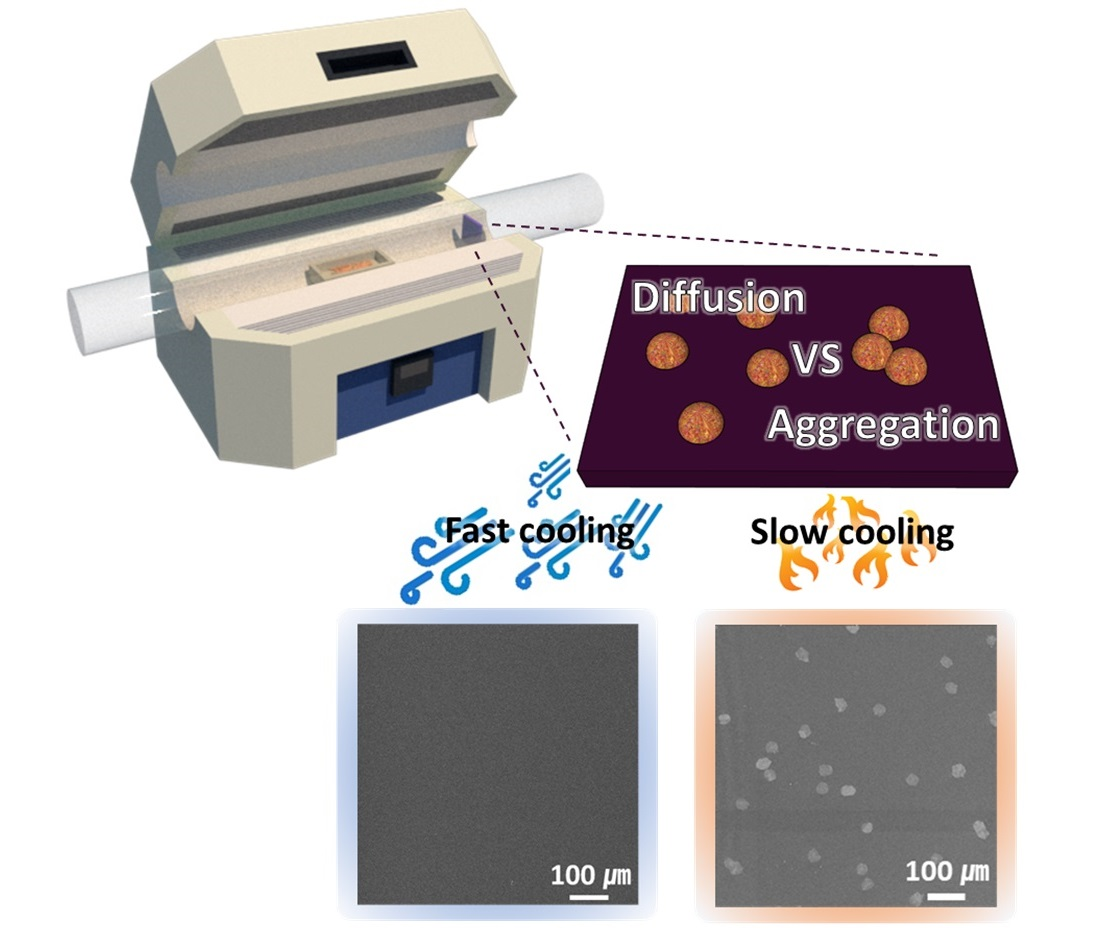
:Organic thin films with smooth surfaces are mandated for high-performance organic electronic devices. Abrupt nucleation and aggregation during film formation are two main factors that forbid smooth surfaces. Here, we report a simple fast cooling (FC) adapted physical vapor deposition (FCPVD) method to produce ultrasmooth organic thin films through effectively suppressing the aggregation of adsorbed molecules. We have found that thermal energy control is essential for the spread of molecules on a substrate by diffusion and it prohibits the unwanted nucleation of adsorbed molecules. FCPVD is employed for cooling the horizontal tube-type organic vapor deposition setup to effectively remove thermal energy applied to adsorbed molecules on a substrate. The organic thin films prepared using the FCPVD method have remarkably ultrasmooth surfaces with less than 0.4 nm root mean square (RMS) roughness on various substrates, even in a low vacuum, which is highly comparable to the ones prepared using conventional high-vacuum deposition methods. Our results provide a deeper understanding of the role of thermal energy employed to substrates during organic film growth using the PVD process and pave the way for cost-effective and high-performance organic devices.

1. Introduction
Organic thin films are an effective material for device applications, such as organic light emitting diodes (OLEDs) and organic photovoltaics [1,2,3,4,5,6]. Developing methods for the deposition of organic thin film has been an important research topic in the material sciences fields for a long time [4,5,6,7,8]. One of many urgent issues regarding organic thin film is to achieve high quality—in terms of surface smoothness—that is largely hindered by the uncontrolled nucleation of target molecules or the formation of irregular aggregates [7,9,10,11,12]. Therefore, inhibiting abrupt nucleation and suppressing aggregates during film formation are two reasonable pathways for the formation of highly smooth films. For these, various approaches have been suggested by many research groups, including the Hu group, who demonstrates two-dimensional molecular crystals with smooth surfaces by space-confined self-assembly in solution [13,14], and the Chi group, who improves the surface roughness by using foreign particles in vapor phase [15].
The most conventional and standard method for the preparation of organic film is to deposit organic vapors under a high-vacuum environment (referred to as the ‘high-vacuum method’) [7,10,16,17,18,19]. A low-vacuum method, represented by physical vapor deposition (PVD) is an alternative [20,21,22,23]. Although the former is used as a standard technique for both industrial and academic research purposes, it is less advantageous than the latter mainly due to the cost required for a high-vacuum environment. Meanwhile, PVD suffers from the lack of understanding and controllability of nucleation and aggregation, which results in the loss of the cost-effectiveness advantage, as it runs under a low-vacuum environment [20,21,22].
Representing an important parameter, the effect of substrate temperature has been widely studied for high-vacuum methods. For example, Chiu and co-workers have reported the anomalous surface roughness change of tris-(8-hydroxyquinoline)aluminum at substrate temperatures between 90 and 120 °C [24]. They show that temperature change induces a thermal interconversion between the meridional and facial isomers, which eventually induces a higher degree of surface smoothness. Further, an amorphous to crystalline phase transformation of rubrene film has been reported by Im and co-workers [25]. Since the studies for the low-vacuum PVD method are relatively less popular, we focus on the parameters for reducing uncontrolled nucleation and aggregation during PVD.
In this report, we show that the aggregation of deposited molecules can be effectively suppressed by employing a fast cooling step in the PVD process (FCPVD). We demonstrate that the simple fast cooling step controls the thermal energy applied to a substrate to suppress nucleation and aggregation during the PVD process. Using this method, ultrasmooth thin films of four molecules—5,6,11,12-tetraphenyltetracene (rubrene), tris(8-hydroxyquinoline)aluminum (Alq3), N,N′-di(1-naphthyl)-N,N′-diphenyl-(1,1′-biphenyl)-4,4′-diamine (NPD), and [6,6]-phenyl-C61-butyric acid methyl ester (PCBM)—are obtained with less than 0.4 nm of root mean square (RMS) roughness. Further, it is confirmed that this method works for various substrates, including Si, Si/SiO2, quartz, mica, and indium tin oxide (ITO). The organic thin films formed through the FCPVD method in low-vacuum (10−2 Torr) conditions show lower RMS roughness than those films obtained using the high-vacuum method (10−6 Torr).
2. Materials and Methods
2.1. Growth of Organic Thin Films
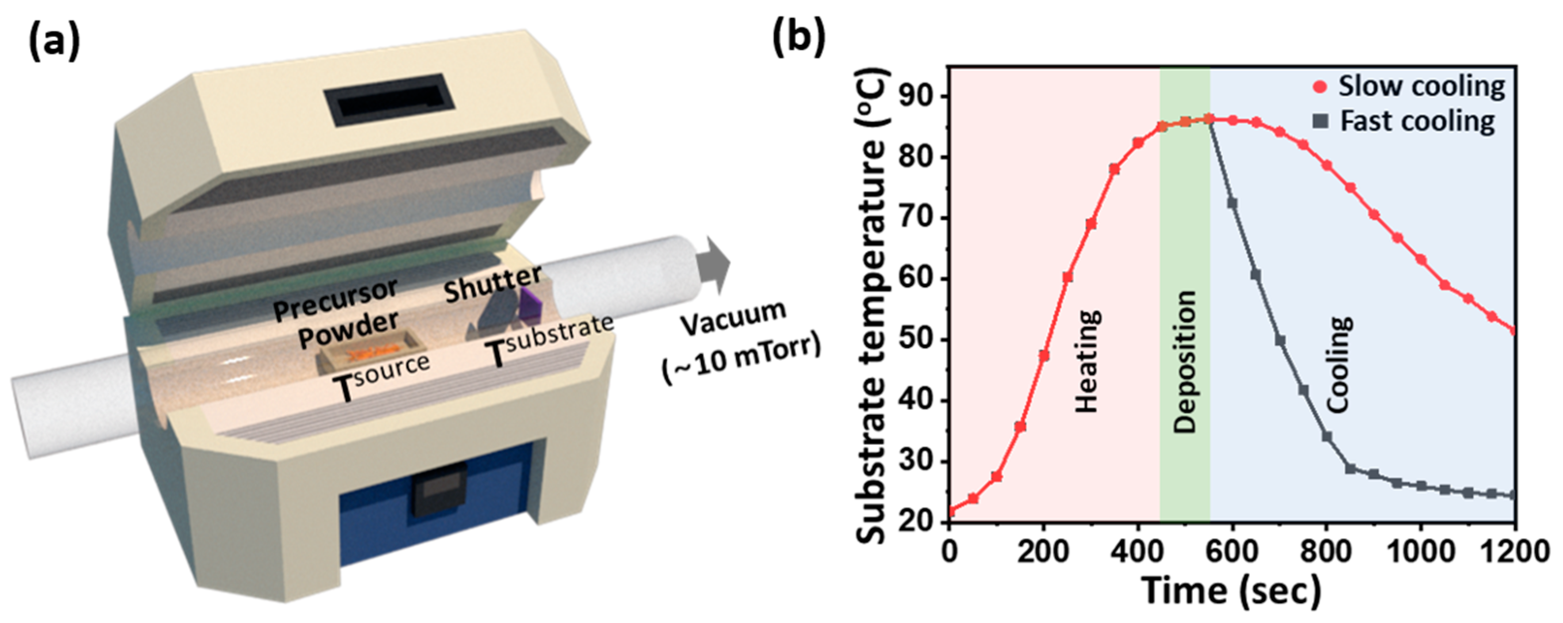
All precursor powders were purchased from commercial sources (5,6,11,12-tetraphenylnaphthacene (rubrene, 98%, Sigma-Aldrich, Darmstadt, Germany), tris-(8-hydroxyquinoline)aluminum (Alq3, 98%, Sigma-Aldrich, Darmstadt, Germany), N,N′-di(1-naphthyl)-N,N′-diphenyl-(1,1′-biphenyl)-4,4′-diamine (NPD, 99%, Tokyo Chemical Industry, Kumagaya, Japan), and [6,6]-phenyl-C61-butyric acid methyl ester (PCBM, 99.5%, Tokyo Chemical Industry, Kumagaya, Japan) and used without further purification. FCPVD is performed using a horizontal tube furnace (TF55035C-1, Lindberg/Blue M, Waltham, Unites States) system (Figure 1a). Approximately 10 mg of precursor powder, loaded in a ceramic boat, is placed at the center of a tube furnace using a quartz protection tube. A substrate, where the organic vapors are to be deposited, is placed in the end region of the furnace where the temperature is naturally decreased. A PVD setup usually results in the end region of the furnace having a lower temperature than the center region. The furnace temperature is increased under low-vacuum conditions (~10−2 Torr) until the precursor powders are vaporized at the target source temperature (Tsource) and deposited on a substrate at the target substrate temperature (Tsubstrate). The target temperature conditions are shown in Table S1. After reaching the target temperatures, the system is maintained for a designated deposition time (Table S1). The vapor supply is stopped after the designated deposition time using a shutter that is set between a precursor boat and a target substrate. The substrate temperature profiles of rubrene are shown in Figure 1b, and those of Alq3, NPD, and PCBM are shown in Figure S1 in the Supplementary Materials. The FCPVD method rapidly lowers substrate temperature by opening up the top cover of the furnace with the air blowing from an electric fan. Conversely, the slow cooling PVD (SCPVD) method lowers the substrate temperature gradually by simply turning off the furnace and closing the top cover. The deposition rate is approximately 1.2 nm/s, as measured from the film thickness. The film thickness is measured using AFM. The deposition time corresponds to the period during which the shutter is open.
The high-vacuum method is attempted using the same precursor powders through thermal evaporation under high-vacuum conditions (~10−6 Torr). Approximately 10 mg of precursor powder is used, with deposition rates of under 0.5 Å/s. Rubrene, Alq3, NPD, and PCBM are vaporized at 170 °C, 200 °C, 190 °C, and 280 °C, respectively, and deposited on Si/SiO2 substrates at Tsubstrate (Table S1) or room temperature (25 °C).
2.2. Characterization of Organic Thin Films
The resulting films are analyzed using scanning electron microscopy (SEM, LYRA3, TESCAN, Brno, Czech) and atomic force microscopy (AFM, NanoScope IIIa, Santa Barbara, United States). Grazing incidence wide-angle X-ray scattering (GIWAXS, Pohang Accelerator Laboratory, Pohang, Korea) patterns of the resulting films are obtained from the 3C beamline at the Pohang Accelerator Laboratory (PAL) to examine the crystallinity of the films. All the measurements are made at room temperature.
2.3. Device Fabrication and Measurement
Organic films are deposited using PVD methods on 30 nm indium tin oxide (ITO)-coated glass substrates sonicated in a series of solvents and blown with N2 gas. The device structures are glass/ 30 nm ITO/ 120 nm Alq3/ 100 nm Al (electron-only device, EOD), glass/ 30 nm ITO/ 120 nm NPD/ 100 nm Al (hole-only device, HOD), and glass/ 30 nm ITO/ 120 nm NPD/ 120 nm Alq3/ 100 nm Al (heterojunction device). Al is deposited through e-beam evaporation (14-SN-004, SNTEK, Suwon, Korea) at 0.5 Å/s under ~10−6 Torr. Current density measurements are carried out at room temperature and in ambient conditions without any protective coatings. The results are obtained using a probe station (M6VC, MS TECH, Seoul, Korea) and a semiconductor analyzer (4200A-SCS, Keithley, Beaverton, United States).
3. Results and Discussion
3.1. Deposition of Ultrasmooth Organic Thin Films
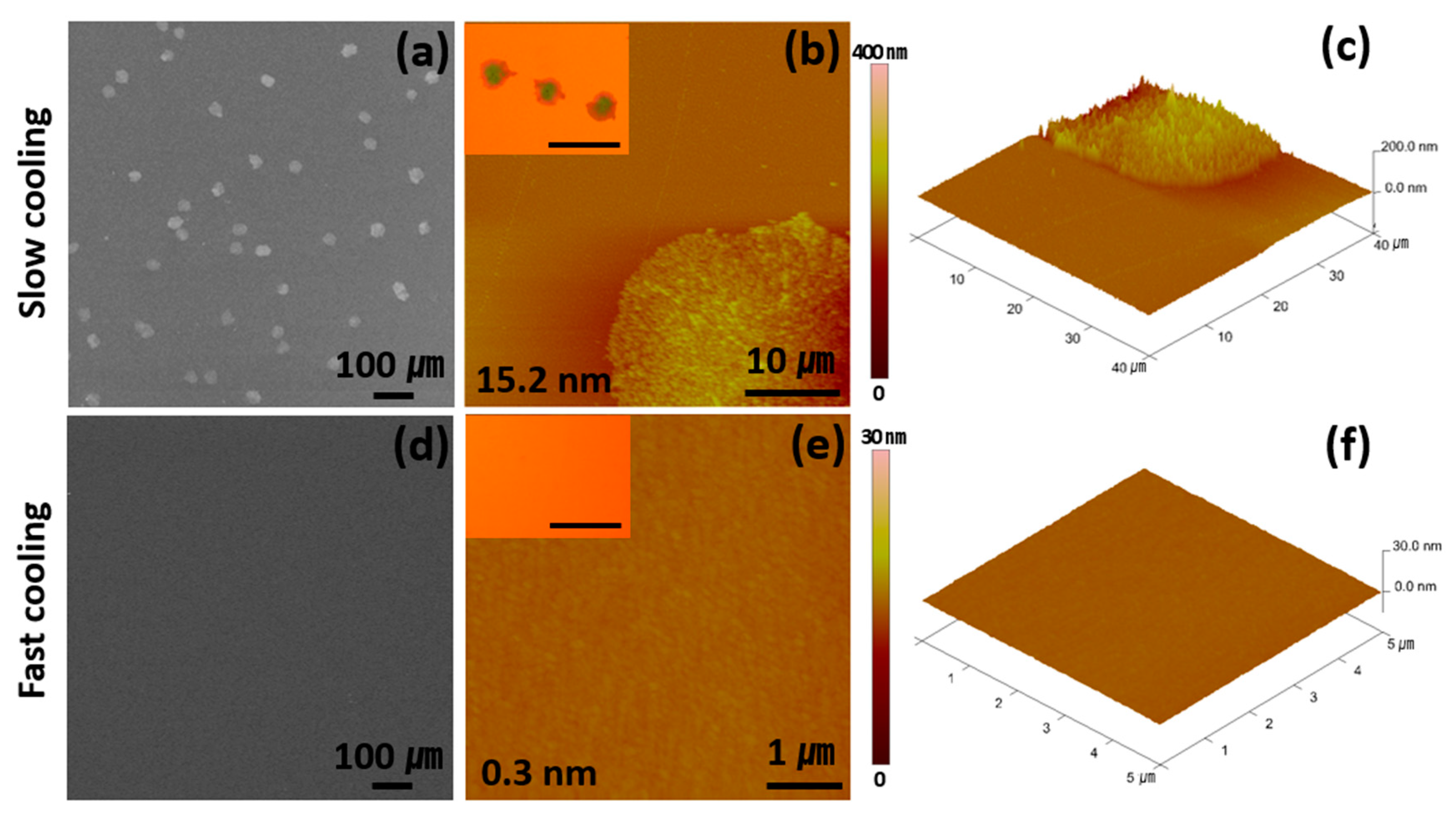
In this study, four organic molecules that are widely applied to organic devices—rubrene, Alq3, NPD, and PCBM—are deposited using a horizontal PVD system (Figure 1a) [26,27,28,29,30,31,32,33]. The PVD system is designed to generate organic vapors at the center of the furnace at Tsource and deposit them on a solid substrate located at the end of the furnace where the temperature is naturally lowered to Tsubstrate. This system allows for the control of Tsource and Tsubstrate, correspondingly, which is important for the manipulation of the degrees of diffusion and the nucleation of adsorbed molecules on a substrate. We have first attempted the deposition of rubrene film using the PVD system. The rubrene films are prepared by following the conventional condition [34,35,36], i.e., rubrene powder is vaporized at a Tsource of 250 °C and deposited on a Si/SiO2 substrate at a Tsubstrate of 85 °C, for various deposition times (10 s, 40 s, 70 s, 100 s, or 130 s). The thickness of each film is approximately 13 nm, 49 nm, 82 nm, 120 nm, and 155 nm, respectively. The thicknesses are measured using AFM. After deposition, the Tsubstrate is cooled down to room temperature by turning off the furnace and closing the top cover, which is referred to as the SCPVD method. The substrate temperature profile indicates that it takes about 600 s to lower the Tsubstrate from 85 to 50 °C (Figure 1b). The resulting films are very rough (over 10 nm of RMS roughness) with a high population of aggregated particles (Figure 2a–c, and S2) regardless of the deposition time, as frequently reported in many previous examples [34,35,37,38]. The presence of aggregated particles indicates that the aggregation of adsorbed molecules is dominant under this condition.
There are two possible origins for the aggregation. The first is an insufficient diffusion of adsorbed molecules to evenly spread the molecules at Tsubstrate before they become aggregated, and the second is residual heat on substrates inducing nucleation, thus growing into aggregated particles [24,36,39,40,41,42]. To evaluate the latter possibility and diminish it, a fast cooling step that drops Tsubstrate down to room temperature in 300 s (Figure 1b) is employed by blowing air through the substrate region using an electric fan after the designated time of deposition. In high contrast to the result of the SCPVD method, smooth surfaces with remarkably reduced aggregates are obtained at a deposition time of 100 s (Figure 2d). To our great surprise, a remarkably ultrasmooth film of rubrene with 0.3 nm of RMS roughness is obtained (Figure 2e,f). This is a remarkable quality of surface roughness considering that the roughness of a bare Si/SiO2 substrate is 0.2 nm of RMS roughness (Figure S3). These results are notable, considering that the previously reported rubrene thin films have a roughness of approximately 0.9 nm [25,37,43]. Therefore, compared with previous studies, it is remarkable that rubrene thin films with 0.3 nm of RMS roughness can be formed through FCPVD in low-vacuum conditions. Furthermore, the thermal stability of rubrene films is tested using annealing rubrene films prepared through FCPVD at 70 °C under Ar for 3 h. The results show that the surface retains high smoothness at this condition (Figure S4), which is in high contrast to the previous result by Park et al. showing a rough surface upon similar treatment [25].
The successful formation of ultrasmooth rubrene film owes mainly to the adequate control of substrate temperature, allowing adsorbed molecules to diffuse on a substrate but prohibiting aggregation or nucleation [24,36,39,40,41,42]. When Tsubstrate is higher than 85 °C for more than 100 s during the slow cooling of the substrate (Figure 1b), very rough surfaces containing aggregates are formed, thus implying that nucleation starts at this condition (Figure 2a–c). This result shows that the high substrate temperature provides energy to overcome the activation energy for nucleation, causing aggregates. These aggregates are significantly reduced by lowering Tsubstrate down to room temperature through fast cooling (Figure 2d–f). However, low Tsubstrate is not the only parameter to consider in avoiding aggregates, as rough surfaces are still formed even at low Tsubstrate (40 °C) values (Figure S5); however, this occurs when the deposition time is not long enough (<100 s) (Figure S6). These results imply that appropriate thermal energy and time are required to evenly spread the molecules on a substrate.
3.2. Versatility of the FCPVD Method Applied to Various Organic Molecules and Substrates
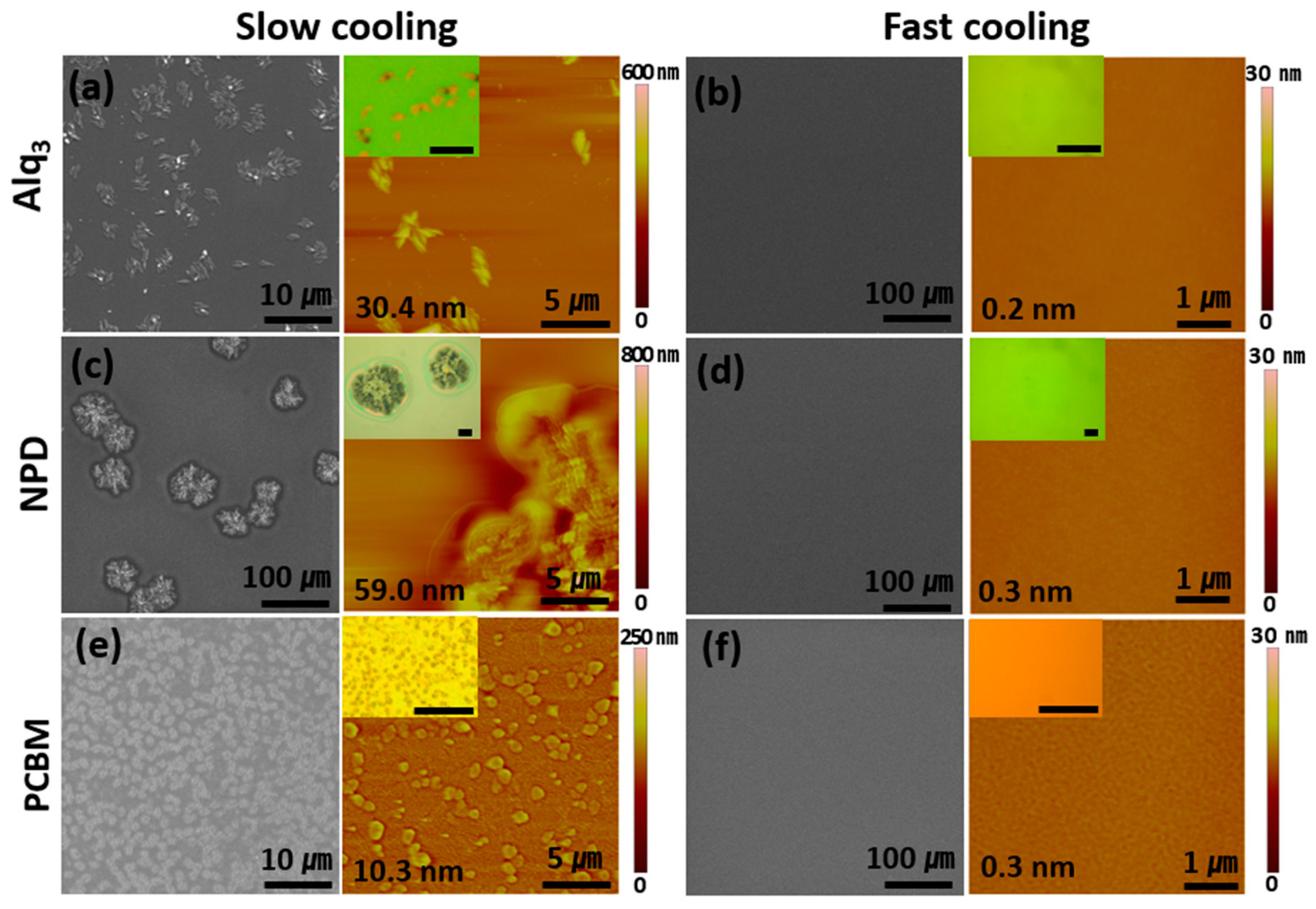
Evaluating the versatility of the FCPVD method has been attempted with other organic molecules (Alq3, NPD, and PCBM), and all the tested molecules show similar results (Figure 3). While the films obtained through the SCPVD method have very rough surfaces (over 10 nm of RMS roughness) with a large population of aggregated particles, those films obtained through the FCPVD method have ultrasmooth surfaces (lower than 0.4 nm of RMS roughness) without particles or notable defects (Figure 3). Furthermore, the FCPVD method has been applied to various substrates, including Si, quartz, mica, and ITO substrates (Figure S3). These results show that the FCPVD method can be applied to various organic molecules and substrates by suppressing nucleation, resulting in ultrasmooth films.
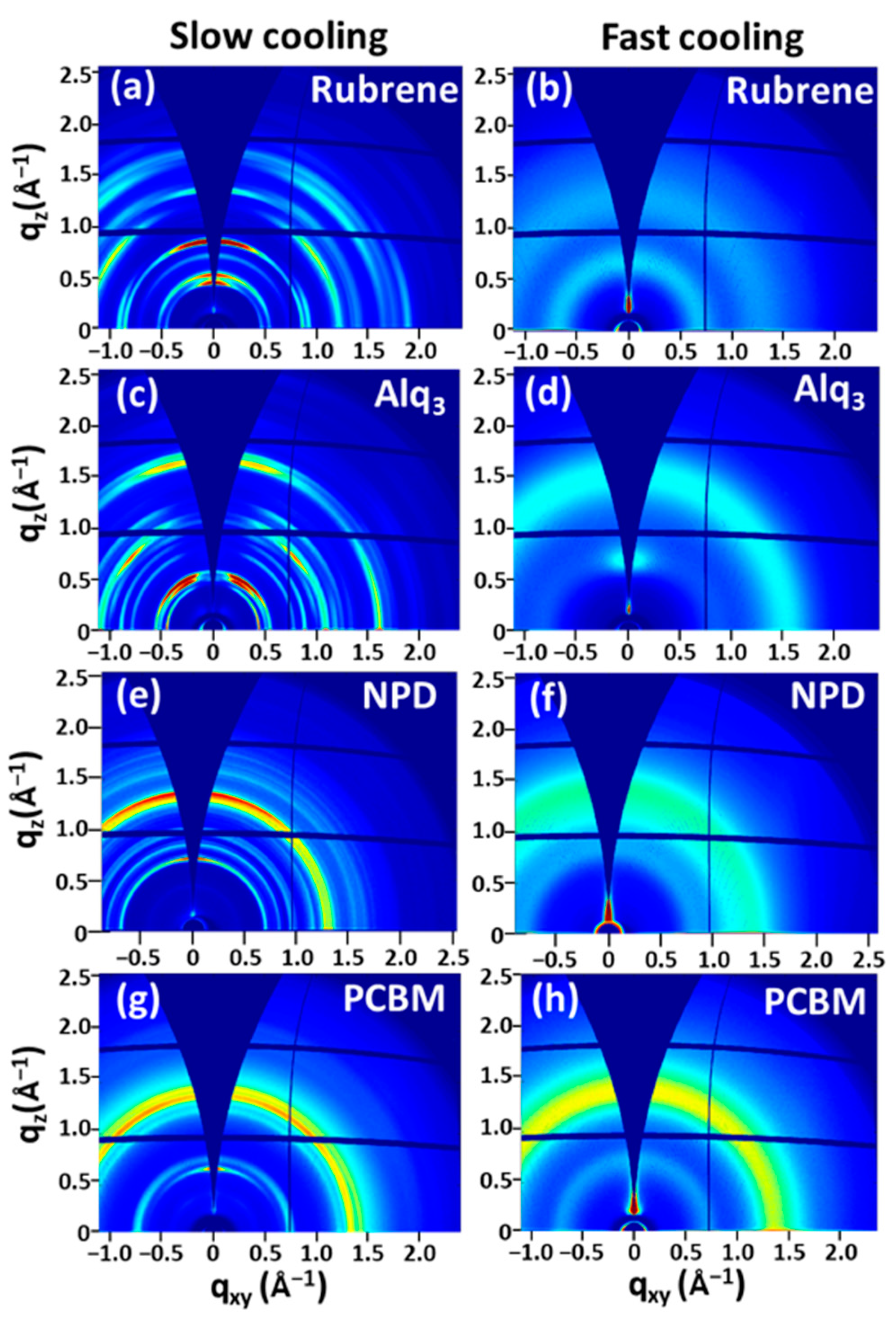
The successful nucleation suppression using the FCPVD method has been confirmed through grazing incidence wide-angle X-ray scattering (GIWAXS) analysis. These results indicate that the rough films are crystalline, while smooth films are amorphous (Figure 4). qxy and qz are the scattering vectors in the plane and out of the plane, respectively. The scattering intensities are represented by colors from high (red) to low (blue). The rubrene film obtained using the SCPVD method shows sharp and anisotropic scattering peaks; when assigned to a mixture of orthorhombic and triclinic phases, thermodynamically favorable crystalline forms from large aggregated particles (Figure 4a) [44,45]. Conversely, the rubrene film grown using the FCPVD method shows broad peaks at q ~0.68 Å−1 with isotropy, thus confirming the kinetically favorable amorphous phase (Figure 4b) [43]. Similar to rubrene films, Alq3, NPD, and PCBM films exhibit nucleation suppression using the FCPVD method (Figure 4d–h), while the films obtained using the SCPVD method exhibit sharp and anisotropic scattering peaks, indicating crystalline phases (Figure 4c–g). The deposited Alq3 and NPD films are characterized to be an α-phase and a triclinic phase, respectively, which are thermodynamically favorable forms [46,47]. Further, the PCBM film is well-matched with PCBM crystalline powder [48]. On the contrary, Alq3, NPD, and PCBM films grown using the FCPVD method show broad scattering peaks, confirming the kinetically favorable amorphous phase (Figure 4d–h) [17,49,50]. These results imply that the nucleation of adsorbed molecules is effectively suppressed by fast cooling the substrate and that this helps the formation of ultrasmooth organic thin films.
3.3. Comparison of the FCPVD and High-Vacuum Method
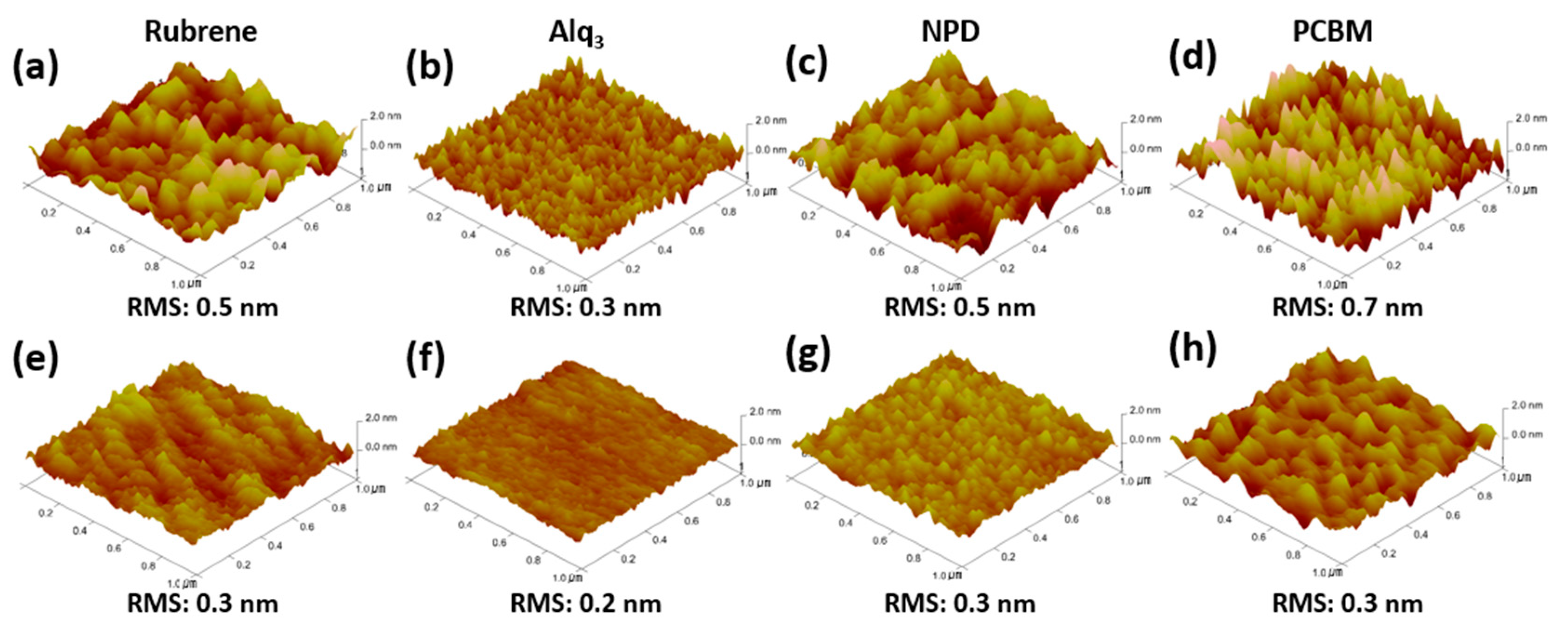
To evaluate the FCPVD method, rubrene, Alq3, NPD, and PCBM films prepared using FCPVD at 85 °C, 88 °C, 88 °C, and 122 °C of Tsubstrate (Table S1), respectively, are directly compared with the ones prepared using the high-vacuum method at the same Tsubstrate condition. The results show that all the films developed using FCPVD (Figure 5) are smoother than the ones developed using the high-vacuum method (Figure S7). Moreover, when depositing such films at room temperature using the high-vacuum method as a standard film growth condition [24,37,43,51,52], the results still show rougher surfaces than the thin films developed using FCPVD (Figure 5 and Table 1). This proves that the FCPVD method is a cost-effective and highly contending method for making ultrasmooth organic films.
3.4. Current Density-Voltage Characteristics of the Films
Among the target molecules in ultrasmooth films, Alq3 and NPD films are semiconductors in an amorphous phase and have been drawing great attention as electron transport layer and hole transport layer in OLED, respectively [53,54,55]. To further evaluate the FCPVD method, the quality of the film prepared using the FCPVD method has been examined with fabricated electron transport layer-only devices (EOD, ITO/Alq3/Al), hole transport layer-only devices (HOD, ITO/NPD/Al), and heterojunction devices (ITO/NPD/Alq3/Al)—which are the basic types of OLEDs—by analyzing the current density–voltage characteristics. All measurements are carried out at room temperature and in ambient conditions without any protective coatings. Before the measurements, the surface morphology of films is checked using AFM. Both Alq3 and NPD films on ITO substrates are very smooth (RMS: 0.2 nm and 0.4 nm, respectively) (Figure S3), and the roughness is maintained (RMS: 0.3 nm) in the heterojunction film, in which NPD and Alq3 thin films have been sequentially deposited on an ITO substrate (Figure S8). All devices fabricated using the FCPVD method exhibit typical current density–voltage curves without short circuits (Figure S9) [53,54,55]. Although the ultrasmooth films are obtained at low-vacuum conditions, the heterojunction device obtained using the FCPVD method shows a similar level of current density to the ones prepared in a high-vacuum system [53,54,55]. In contrast, all devices obtained using the SCPVD method are shorted because of the presence of aggregated particles in the film (Figure S10) [56,57]. These results support that the FCPVD method is effective for OLED fabrication, even with a cost-effective low-pressure system.
4. Conclusions
In summary, we show that the fast cooling of substrates during the PVD process results in the ultrasmooth surfaces of diverse organic films via aggregation suppression. The FCPVD method effectively removes residual heat on a substrate to prohibit nucleation, as it causes adsorbed molecules to diffuse to avoid nucleation. All the organic films grown using the FCPVD method have ultrasmooth surfaces, with less than 0.4 nm of RMS roughness on various substrates. Additionally, the organic thin films, obtained using the FCPVD method and made in low-vacuum conditions, exhibit smoother surfaces than ones formed using the conventional vapor deposition method in high-vacuum conditions. Considering the versatility of organic molecules and substrates and the usage of inexpensive low-vacuum conditions, this simple and effective method will contribute to the fabrication of low-cost, high-performance organic devices, as well as an understanding of organic thin film growth.
Supplementary Materials
The following are available online at https://0-www-mdpi-com.brum.beds.ac.uk/article/10.3390/ma14237247/s1, Figure S1: substrate temperature profiles of Alq3, NPD, and PCBM depending on SCPVD method and FCPVD method, Figure S2: SEM and AFM images of rubrene films on Si/SiO2 substrate obtained by SCPVD method depending on various deposition times, Figure S3: AFM images of rubrene, Alq3, NPD, and PCBM films on Si/SiO2, Si, quartz, mica, and ITO substrates obtained by FCPVD method, Figure S4: AFM images of rubrene film by FCPVD, Figure S5: AFM images of rubrene films on the Si/SiO2 substrate obtained at low substrate temperature (40 °C) condition depending on deposition time, Figure S6: surface morphologies of rubrene films on the Si/SiO2 substrate obtained by FCPVD method depending on deposition time, Figure S7: optical microscope images of rubrene, Alq3, NPD, and PCBM films on Si/SiO2 substrates by the high-vacuum method, Figure S8: AFM images of heterojunction film in which NPD and Alq3 thin films were sequentially deposited on an ITO substrate by FCPVD, Figure S9: the current density-voltage characteristics of the devices prepared with ultrasmooth films obtained by FCPVD method, Figure S10: optical microscope images of NPD, Alq3, and NPD/Alq3 films on ITO substrates, Table S1: the target temperature conditions and deposition time for ultrasmooth films.
Author Contributions
Methodology, data curation, writing—original draft preparation, and visualization, Y.Y.; conceptualization, J.L.; visualization and investigation, S.L. and S.K.; conceptualization, supervision, validation, writing–reviewing, and editing, H.C.C. All authors have read and agreed to the published version of the manuscript.
Funding
This work was supported by the Veteran Researcher Grant (No. 2019R1A2C2004259), managed by the National Research Foundation of Korea (NRF) and Samsung Electronics.
Institutional Review Board Statement
Not applicable.
Informed Consent Statement
Not applicable.
Data Availability Statement
The authors confirm that the data supporting the findings of this study are available within the article.
Acknowledgments
For the structure analysis, grazing incidence wide-angle X-ray scattering patterns were obtained at the 3C beamline of Pohang Accelerator Laboratory (PAL, South Korea).
Conflicts of Interest
The authors declare no conflict of interest.
References
- Swayamprabha, S.S.; Dubey, D.K.; Song, W.-C.; Lin, Y.-T.; Yadav, R.A.K.; Singh, M.; Jou, J.-H. An Approach for Measuring the Dielectric Strength of OLED Materials. Materials 2018, 11, 979. [Google Scholar] [CrossRef] [PubMed] [Green Version]
- Jesuraj, P.J.; Jeganathan, K. Surface defects impeded excitons in Alq3 based heterojunction OLEDs. Appl. Surf. Sci. 2013, 268, 323–326. [Google Scholar] [CrossRef]
- Bi, Y.-G.; Feng, J.; Ji, J.-H.; Chen, Y.; Liu, Y.-S.; Li, Y.-F.; Liu, Y.-F.; Zhang, X.-L.; Sun, H.-B. Ultrathin and ultrasmooth Au films as transparent electrodes in ITO-free organic light-emitting devices. Nanoscale 2016, 8, 10010–10015. [Google Scholar] [CrossRef]
- Song, B.; Forrest, S.R. Nanoscale Control of Morphology in Fullerene-Based Electron-Conducting Buffers via Organic Vapor Phase Deposition. Nano Lett. 2016, 16, 3905–3910. [Google Scholar] [CrossRef] [PubMed]
- Ye, L.; Jiao, X.; Zhou, M.; Zhang, S.; Yao, H.; Zhao, W.; Xia, A.; Ade, H.; Hou, J. Manipulating Aggregation and Molecular Orientation in All-Polymer Photovoltaic Cells. Adv. Mater. 2015, 27, 6046–6054. [Google Scholar] [CrossRef] [PubMed]
- Zhang, T.; Han, H.; Zou, Y.; Lee, Y.-C.; Oshima, H.; Wong, K.-T.; Holmes, R.J. Impact of Thermal Annealing on Organic Photovoltaic Cells Using Regioisomeric Donor–Acceptor–Acceptor Molecules. ACS Appl. Mater. Interfaces 2017, 9, 25418–25425. [Google Scholar] [CrossRef]
- Qu, B.; Ding, K.; Sun, K.; Hou, S.; Morris, S.; Shtein, M.; Forrest, S.R. Fast Organic Vapor Phase Deposition of Thin Films in Light-Emitting Diodes. ACS Nano 2020, 14, 14157–14163. [Google Scholar] [CrossRef] [PubMed]
- Diao, Y.; Tee, B.C.-K.; Giri, G.; Xu, J.; Kim, D.H.; Becerril, H.A.; Stoltenberg, R.M.; Lee, T.H.; Xue, G.; Mannsfeld, S.C.B. Solution coating of large-area organic semiconductor thin films with aligned single-crystalline domains. Nat. Mater. 2013, 12, 665–671. [Google Scholar] [CrossRef]
- Zhang, Y.; Glor, E.C.; Li, M.; Liu, T.; Wahid, K.; Zhang, W.; Riggleman, R.A.; Fakhraai, Z. Long-range correlated dynamics in ultra-thin molecular glass films. J. Chem. Phys. 2016, 145, 114502. [Google Scholar] [CrossRef] [Green Version]
- Samanta, S.; Huang, G.; Gao, G.; Zhang, Y.; Zhang, A.; Wolf, S.; Woods, C.N.; Jin, Y.; Walsh, P.J.; Fakhraai, Z. Exploring the Importance of Surface Diffusion in Stability of Vapor-Deposited Organic Glasses. J. Phys. Chem. B 2019, 123, 4108–4117. [Google Scholar] [CrossRef]
- Hlawacek, G.; Khokhar, F.S.; Van Gastel, R.; Poelsema, B.; Teichert, C. Smooth Growth of Organic Semiconductor Films on Graphene for High-Efficiency Electronics. Nano Lett. 2011, 11, 333–337. [Google Scholar] [CrossRef] [PubMed]
- Fusella, M.A.; Schreiber, F.; Abbasi, K.; Kim, J.J.; Briseno, A.L.; Rand, B.P. Homoepitaxy of Crystalline Rubrene Thin Films. Nano Lett. 2017, 17, 3040–3046. [Google Scholar] [CrossRef]
- Yao, J.Y.; Zhang, Y.Z.; Tian, X.T.; Zhang, X.Z.; Zhao, H.Z.; Zhang, X.Z.; Jie, J.J.; Wang, X.W.; Li, R.L.; Hu, W. Layer-Defining Strategy to Grow Two-Dimensional Molecular Crystals on a Liquid Surface down to the Monolayer Limit. Angew. Chem. Int. Ed. 2019, 58, 16082–16086. [Google Scholar] [CrossRef]
- Wang, Q.; Yang, F.; Zhang, Y.; Chen, M.; Zhang, X.; Lei, S.; Li, R.; Hu, W. Space-Confined Strategy toward Large-Area Two-Dimensional Single Crystals of Molecular Materials. J. Am. Chem. Soc. 2018, 140, 5339–5342. [Google Scholar] [CrossRef]
- Hu, X.; Wang, Z.; Zhu, X.; Zhu, T.; Zhang, X.; Dong, B.; Huang, L.; Chi, L. Foreign Particle Promoted Crystalline Nucleation for Growing High-Quality Ultrathin Rubrene Films. Small 2016, 12, 4086–4092. [Google Scholar] [CrossRef]
- Sarkar, I.; Laux, M.; Demokritova, J.; Ruffing, A.; Mathias, S.; Wei, J.; Solovyeva, V.; Rudloff, M.; Naghavi, S.S.; Felser, C.; et al. Evaporation temperature-tuned physical vapor deposition growth engineering of one-dimensional non-Fermi liquid tetrathiofulvalene tetracyanoquinodimethane thin films. Appl. Phys. Lett. 2010, 97, 111906. [Google Scholar] [CrossRef]
- Bagchi, K.; Jackson, N.E.; Gujral, A.; Huang, C.; Toney, M.F.; Yu, L.; de Pablo, J.J.; Ediger, M.D. Origin of Anisotropic Molecular Packing in Vapor-Deposited Alq3 Glasses. J. Phys. Chem. Lett. 2018, 10, 164–170. [Google Scholar] [CrossRef]
- Bangsund, J.S.; Hershey, K.W.; Holmes, R.J. Isolating Degradation Mechanisms in Mixed Emissive Layer Organic Light-Emitting Devices. ACS Appl. Mater. Interfaces 2018, 10, 5693–5699. [Google Scholar] [CrossRef]
- Ding, B.-F.; Hou, X.-Y.; Alameh, K. High contrast tandem organic light emitting devices. Appl. Phys. Lett. 2012, 101, 133305. [Google Scholar] [CrossRef] [Green Version]
- Shtein, M.; Gossenberger, H.F.; Benziger, J.B.; Forrest, S.R. Material transport regimes and mechanisms for growth of molecular organic thin films using low-pressure organic vapor phase deposition. J. Appl. Phys. 2001, 89, 1470–1476. [Google Scholar] [CrossRef]
- Xiao, Y.; Zhang, L.; Peng, F.; Pan, G.-B. Fabrication of a cobalt phthalocyanine free-standing film on an ionic liquid surface for memory device applications. RSC Adv. 2018, 8, 5344–5349. [Google Scholar] [CrossRef] [Green Version]
- Zhang, Y.; Diao, Y.; Lee, H.; Mirabito, T.J.; Johnson, R.W.; Puodziukynaite, E.; John, J.; Carter, K.R.; Emrick, T.; Mannsfeld, S.C.B.; et al. Intrinsic and Extrinsic Parameters for Controlling the Growth of Organic Single-Crystalline Nanopillars in Photovoltaics. Nano Lett. 2014, 14, 5547–5554. [Google Scholar] [CrossRef]
- Lee, C.-H.; Schiros, T.; Santos, E.J.G.; Kim, B.; Yager, K.G.; Kang, S.J.; Lee, S.; Yu, J.; Watanabe, K.; Taniguchi, T.; et al. Epitaxial Growth of Molecular Crystals on van der Waals Substrates for High-Performance Organic Electronics. Adv. Mater. 2014, 26, 2812–2817. [Google Scholar] [CrossRef] [PubMed]
- Jian, Z.-A.; Luo, Y.-Z.; Chung, J.-M.; Tang, S.-J.; Kuo, M.-C.; Shen, J.-L.; Chiu, K.-C.; Yang, C.-S.; Chou, W.-C.; Dai, C.-F.; et al. Effects of isomeric transformation on characteristics of Alq3 amorphous layers prepared by vacuum deposition at various substrate temperatures. J. Appl. Phys. 2007, 101, 123708. [Google Scholar] [CrossRef] [Green Version]
- Park, S.-W.; Choi, J.-M.; Lee, K.H.; Yeom, H.W.; Im, S.; Lee, Y.K. Amorphous-to-Crystalline Phase Transformation of Thin Film Rubrene. J. Phys. Chem. B 2010, 114, 5661–5665. [Google Scholar] [CrossRef]
- Li, Z.; Du, J.; Tang, Q.; Wang, F.; Xu, J.-B.; Yu, J.C.; Miao, Q. Induced Crystallization of Rubrene in Thin-Film Transistors. Adv. Mater. 2010, 22, 3242–3246. [Google Scholar] [CrossRef] [PubMed]
- Pinto, R.M. Photocurrent Generation in Bulk vs Bilayer Devices: Quantum Treatment of Model Rubrene/7,7,8,8-Tetracyanoquinodimethane Heterojunctions for Organic Solar Cells. J. Phys. Chem. C 2014, 118, 2287–2297. [Google Scholar] [CrossRef]
- Kao, P.-C.; Chiu, C.-T. MoO3 as p-type dopant for Alq3-based p–i–n homojunction organic light-emitting diodes. Org. Electron. 2015, 26, 443–450. [Google Scholar] [CrossRef]
- Schweicher, G.; Garbay, G.; Jouclas, R.; Vibert, F.; Devaux, F.; Geerts, Y.H. Molecular Semiconductors for Logic Operations: Dead-End or Bright Future? Adv. Mater. 2020, 32, 1905909. [Google Scholar] [CrossRef]
- Rohloff, R.; Kotadiya, N.B.; Crăciun, N.I.; Blom, P.W.M.; Wetzelaer, G.A.H. Electron and hole transport in the organic small molecule α-NPD. Appl. Phys. Lett. 2017, 110, 073301. [Google Scholar] [CrossRef]
- Esaki, Y.; Komino, T.; Matsushima, T.; Adachi, C. Enhanced Electrical Properties and Air Stability of Amorphous Organic Thin Films by Engineering Film Density. J. Phys. Chem. Lett. 2017, 8, 5891–5897. [Google Scholar] [CrossRef]
- Barzegar, H.R.; Larsen, C.; Boulanger, N.; Zettl, A.; Edman, L.; Wågberg, T. Self-Assembled PCBM Nanosheets: A Facile Route to Electronic Layer-on-Layer Heterostructures. Nano Lett. 2018, 18, 1442–1447. [Google Scholar] [CrossRef]
- Pinto, R.M.; Maçôas, E.M.S.; Alves, H. Enhanced conductivity and photoresponse at a rubrene single-crystal–PCBM film interface. J. Mater. Chem. C 2014, 2, 3639–3644. [Google Scholar] [CrossRef]
- Luo, Y.; Brun, M.; Rannou, P.; Grevin, B. Growth of Rubrene thin film, spherulites and nanowires on SiO2. Phys. Status Solidi (a) 2007, 204, 1851–1855. [Google Scholar] [CrossRef]
- Hsu, C.H.; Deng, J.; Staddon, C.R.; Beton, P.H. Growth front nucleation of rubrene thin films for high mobility organic transistors. Appl. Phys. Lett. 2007, 91, 193505. [Google Scholar] [CrossRef]
- Käfer, D.; Witte, G. Growth of crystalline rubrene films with enhanced stability. Phys. Chem. Chem. Phys. 2005, 7, 2850–2853. [Google Scholar] [CrossRef] [PubMed]
- Park, S.-W.; Hwang, J.M.; Choi, J.-M.; Hwang, D.K.; Oh, M.S.; Kim, J.H.; Im, S. Rubrene thin-film transistors with crystalline and amorphous channels. Appl. Phys. Lett. 2007, 90, 153512. [Google Scholar] [CrossRef]
- Park, B.; In, I.; Gopalan, P.; Evans, P.G.; King, S.; Lyman, P.F. Enhanced hole mobility in ambipolar rubrene thin film transistors on polystyrene. Appl. Phys. Lett. 2008, 92, 133302. [Google Scholar] [CrossRef] [Green Version]
- Marchetto, H.; Schmidt, T.; Groh, U.; Maier, F.C.; Lévesque, P.L.; Fink, R.H.; Freund, H.-J.; Umbach, E. Direct observation of epitaxial organic film growth: Temperature-dependent growth mechanisms and metastability. Phys. Chem. Chem. Phys. 2015, 17, 29150–29160. [Google Scholar] [CrossRef] [PubMed] [Green Version]
- Fielitz, T.R.; Holmes, R.J. Crystal Morphology and Growth in Annealed Rubrene Thin Films. Cryst. Growth Des. 2016, 16, 4720–4726. [Google Scholar] [CrossRef]
- Vergnat, C.; Landais, V.; Legrand, J.-F.; Brinkmann, M. Orienting Semiconducting Nanocrystals on Nanostructured Polycarbonate Substrates: Impact of Substrate Temperature on Polymorphism and In-Plane Orientation. Macromolecules 2011, 44, 3817–3827. [Google Scholar] [CrossRef]
- Ferguson, A.J.; Jones, T.S. Photophysics of PTCDA and Me-PTCDI Thin Films: Effects of Growth Temperature. J. Phys. Chem. B 2006, 110, 6891–6898. [Google Scholar] [CrossRef] [PubMed]
- Kowarik, S.; Gerlach, A.; Sellner, S.; Schreiber, F.; Pflaum, J.; Cavalcanti, L.; Konovalov, O. Anomalous roughness evolution of rubrene thin films observed in real time during growth. Phys. Chem. Chem. Phys. 2006, 8, 1834–1836. [Google Scholar] [CrossRef]
- Jurchescu, O.D.; Meetsma, A.; Palstra, T.T.M. Low-temperature structure of rubrene single crystals grown by vapor transport. Acta Crystallogr. Sect. B Struct. Sci. 2006, 62, 330–334. [Google Scholar] [CrossRef] [Green Version]
- Huang, L.; Liao, Q.; Shi, Q.; Fu, H.; Ma, J.; Yao, J. Rubrene micro-crystals from solution routes: Their crystallography, morphology and optical properties. J. Mater. Chem. 2009, 20, 159–166. [Google Scholar] [CrossRef]
- Fukushima, T.; Kaji, H. Green- and blue-emitting tris(8-hydroxyquinoline) aluminum(III) (Alq3) crystalline polymorphs: Preparation and application to organic light-emitting diodes. Org. Electron. 2012, 13, 2985–2990. [Google Scholar] [CrossRef]
- Cheng, J.-A.; Cheng, P.-J. Crystal Study of N,N′-diphenyl-N,N′-bis(1-naphthyl)-1,1′-biphenyl-4,4′-diamine. J. Chem. Crystallogr. 2010, 40, 557–560. [Google Scholar] [CrossRef]
- Sun, Y.; Onwona-Agyeman, B.; Miyasato, T. Properties of Charge Carrier Transport in Au/Phenyl C61 Butyric Acid Methyl Ester/Au Structure. Jpn. J. Appl. Phys. 2011, 50, 031601. [Google Scholar] [CrossRef]
- Leung, Y.H.; Djurišić, A.B.; Cheung, C.H.; Xie, M.H.; Chan, W.K. Growth of N,N′-di(naphthalene-1-yl)-N,N′-diphenyl-benzidine dome structures. J. Appl. Phys. 2005, 97, 033515. [Google Scholar] [CrossRef] [Green Version]
- Chikamatsu, M.; Nagamatsu, S.; Yoshida, Y.; Saito, K.; Yase, K.; Kikuchi, K. Solution-processed n-type organic thin-film transistors with high field-effect mobility. Appl. Phys. Lett. 2005, 87, 203504. [Google Scholar] [CrossRef] [Green Version]
- Wang, M.-H.; Konya, T.; Yahata, M.; Sawada, Y.; Kishi, A.; Uchida, T.; Lei, H.; Hoshi, Y.; Sun, L.-X. Thermal change of organic light-emitting ALQ3 thin films. J. Therm. Anal. Calorim. 2009, 99, 117–122. [Google Scholar] [CrossRef]
- Kumar, A.; Li, G.; Hong, Z.; Yang, Y. High efficiency polymer solar cells with vertically modulated nanoscale morphology. Nanotechnology 2009, 20, 165202. [Google Scholar] [CrossRef] [PubMed] [Green Version]
- Juhasz, P.; Nevrela, J.; Micjan, M.; Novota, M.; Uhrik, J.; Stuchlikova, L.; Jakabovic, J.; Harmatha, L.; Weis, M. Charge injection and transport properties of an organic light-emitting diode. Beilstein J. Nanotechnol. 2016, 7, 47–52. [Google Scholar] [CrossRef] [PubMed] [Green Version]
- Weis, M.; Otsuka, T.; Taguchi, D.; Manaka, T.; Iwamoto, M. Charge injection and accumulation in organic light-emitting diode with PEDOT:PSS anode. J. Appl. Phys. 2015, 117, 155503. [Google Scholar] [CrossRef]
- Taguchi, D.; Weis, M.; Manaka, T.; Iwamoto, M. Probing of carrier behavior in organic electroluminescent diode using electric field induced optical second-harmonic generation measurement. Appl. Phys. Lett. 2009, 95, 263310. [Google Scholar] [CrossRef]
- Nagai, M. Impact of Particulate Contaminants on the Current Leakage Defect in OLED Devices. J. Electrochem. Soc. 2007, 154, J387. [Google Scholar] [CrossRef]
- Oostra, A.J.; Blom, P.W.; Michels, J.J. Prevention of short circuits in solution-processed OLED devices. Org. Electron. 2014, 15, 1166–1172. [Google Scholar] [CrossRef]
Figure 1.
Experimental scheme and substrate temperature profile. (a) Schematic view of the horizontal PVD system used to obtain organic thin films. (b) Substrate temperature profiles of rubrene film using the SCPVD method (red) and the FCPVD method (grey) when the deposition time is 100 s.
Figure 1.
Experimental scheme and substrate temperature profile. (a) Schematic view of the horizontal PVD system used to obtain organic thin films. (b) Substrate temperature profiles of rubrene film using the SCPVD method (red) and the FCPVD method (grey) when the deposition time is 100 s.

Figure 2.
SEM and AFM images of rubrene films, depending on the cooling rate. The upper row images (a–c) and the lower row images (d–f) are obtained using SCPVD and FCPVD, respectively, when the deposition time is 100 s. The insets are OM images of each film (scale bar: 50 μm).
Figure 2.
SEM and AFM images of rubrene films, depending on the cooling rate. The upper row images (a–c) and the lower row images (d–f) are obtained using SCPVD and FCPVD, respectively, when the deposition time is 100 s. The insets are OM images of each film (scale bar: 50 μm).

Figure 3.
Various organic films, depending on the cooling rate of the substrate. SEM and AFM images of (a,b) Alq3 films, (c,d) NPD films, and (e,f) PCBM films, depending on the cooling rate. The films on the left side (a, c, and e) and those on the right side (b, d, and f) are obtained using SCPVD and FCPVD methods, respectively. The insets are optical microscope images of each film (scale bar: 10 μm).

Figure 4.
Structure analysis of organic thin films. GIWAXS patterns of (a,b) rubrene films, (c,d) Alq3 films, (e,f) NPD films, and (g,h) PCBM films grown using the SCPVD (left column) and FCPVD (right column) methods.
Figure 4.
Structure analysis of organic thin films. GIWAXS patterns of (a,b) rubrene films, (c,d) Alq3 films, (e,f) NPD films, and (g,h) PCBM films grown using the SCPVD (left column) and FCPVD (right column) methods.

Figure 5.
Surface morphologies of various organic thin films, depending on the deposition method. AFM images of (a,e) rubrene, (b,f) Alq3, (c,g) NPD, and (d,h) PCBM films on Si/SiO2 substrates. The films in the upper row of AFM images (a–d) and those in the lower row (e–h) are obtained using the high-vacuum method and FCPVD, respectively.


Table 1.
RMS roughness of various organic thin films, depending on the deposition method.
| Rubrene | Alq3 | NPD | PCBM | |
|---|---|---|---|---|
| High-vacuum method (10−6 Torr) | 0.63 ± 0.075 nm | 0.35 ± 0.040 nm | 0.58 ± 0.055 nm | 0.73 ± 0.038 nm |
| FCPVD (10−2 Torr) | 0.33 ± 0.038 nm | 0.22 ± 0.030 nm | 0.35 ± 0.040 nm | 0.35 ± 0.040 nm |
RMS roughness of each film is obtained from 6 samples.
Publisher’s Note: MDPI stays neutral with regard to jurisdictional claims in published maps and institutional affiliations. |
© 2021 by the authors. Licensee MDPI, Basel, Switzerland. This article is an open access article distributed under the terms and conditions of the Creative Commons Attribution (CC BY) license (https://creativecommons.org/licenses/by/4.0/).
Share and Cite
MDPI and ACS Style
Yoon, Y.; Lee, J.; Lee, S.; Kim, S.; Choi, H.C. Ultrasmooth Organic Films Via Efficient Aggregation Suppression by a Low-Vacuum Physical Vapor Deposition. Materials 2021, 14, 7247. https://0-doi-org.brum.beds.ac.uk/10.3390/ma14237247
AMA Style
Yoon Y, Lee J, Lee S, Kim S, Choi HC. Ultrasmooth Organic Films Via Efficient Aggregation Suppression by a Low-Vacuum Physical Vapor Deposition. Materials. 2021; 14(23):7247. https://0-doi-org.brum.beds.ac.uk/10.3390/ma14237247
Chicago/Turabian StyleYoon, Youngkwan, Jinho Lee, Seulgi Lee, Soyoung Kim, and Hee Cheul Choi. 2021. "Ultrasmooth Organic Films Via Efficient Aggregation Suppression by a Low-Vacuum Physical Vapor Deposition" Materials 14, no. 23: 7247. https://0-doi-org.brum.beds.ac.uk/10.3390/ma14237247
Note that from the first issue of 2016, this journal uses article numbers instead of page numbers. See further details here.