
Manufacturing of Complex Silicon–Carbon Structures: Exploring SixCy Materials


Abstract
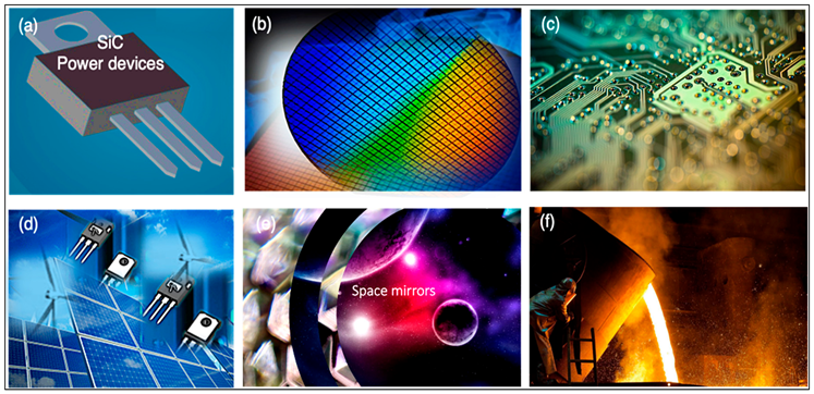
:1. Introduction
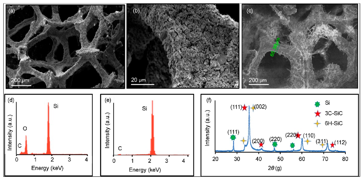
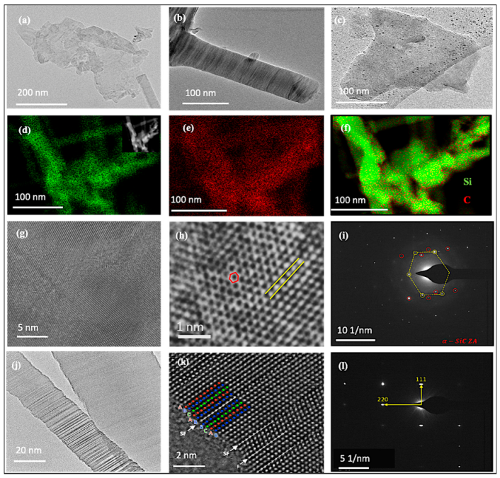
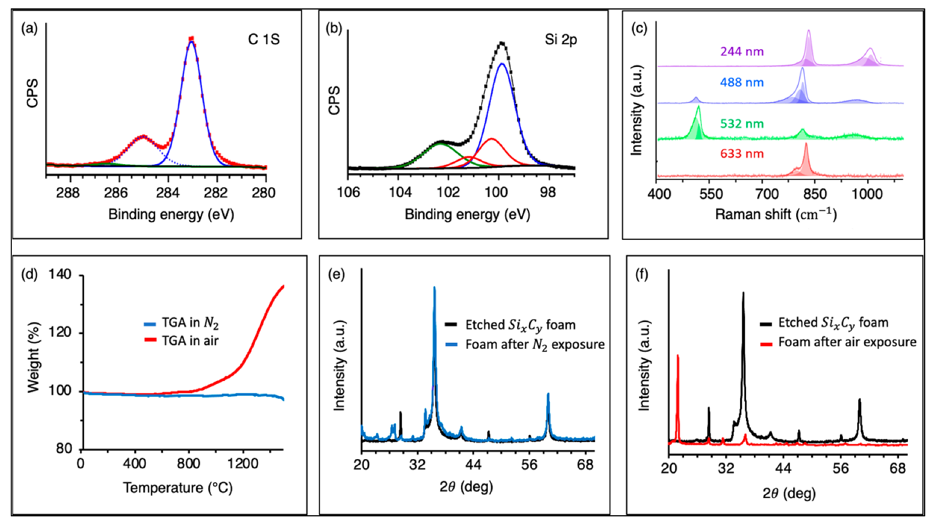
2. Results and Discussion
3. Conclusions
4. Experimental Procedure
Supplementary Materials
Author Contributions
Funding
Acknowledgments
Conflicts of Interest
References
- Melinon, P.; Masenelli, B.; Tournus, F.; Perez, A.; Mélinon, P.; Masenelli, B.; Tournus, F.; Perez, A.; Melinon, P.; Masenelli, B.; et al. Playing with Carbon and Silicon at the Nanoscale. Nat. Mater. 2007, 6, 479–490. [Google Scholar] [CrossRef] [PubMed]
- Akinwande, D.; Huyghebaert, C.; Wang, C.H.; Serna, M.I.; Goossens, S.; Li, L.J.; Wong, H.S.P.; Koppens, F.H.L. Graphene and Two-Dimensional Materials for Silicon Technology. Nature 2019, 573, 507–518. [Google Scholar] [CrossRef] [PubMed]
- Le Ferrand, H.; Chabi, S.; Agarwala, S. 3D Assembly of Graphene Nanomaterials for Advanced Electronics. Adv. Intell. Syst. 2020, 2, 1900151. [Google Scholar] [CrossRef]
- Schwierz, F. Graphene Transistors. Nat. Nanotechnol. 2010, 5, 487–496. [Google Scholar] [CrossRef]
- Guzman, J.; Stern, S. Where Is Silicon Valley? Science 2015, 347, 606–609. [Google Scholar] [CrossRef]
- Mayer, A.S.; Kirkpatrick, B.C. Silicon Photonics. Front. Mod. Opt. 2016, 24, 189–205. [Google Scholar]
- Thompson, S.E.; Parthasarathy, S. Moore’s Law: The Future of Si Microelectronics. Mater. Today 2006, 9, 20–25. [Google Scholar] [CrossRef]
- Wen, D.L.; Sun, D.H.; Huang, P.; Huang, W.; Su, M.; Wang, Y.; Di Han, M.; Kim, B.; Brugger, J.; Zhang, H.X.; et al. Recent Progress in Silk Fibroin-Based Flexible Electronics. Microsyst. Nanoeng. 2021, 7, 35. [Google Scholar] [CrossRef]
- Nagy, R.; Widmann, M.; Niethammer, M.; Dasari, D.B.R.; Gerhardt, I.; Soykal, Ö.O.; Radulaski, M.; Ohshima, T.; Vučković, J.; Son, N.T.; et al. Quantum Properties of Dichroic Silicon Vacancies in Silicon Carbide. Phys. Rev. Appl. 2018, 9, 034022. [Google Scholar] [CrossRef] [Green Version]
- de Leon, N.P.; Itoh, K.M.; Kim, D.; Mehta, K.K.; Northup, T.E.; Paik, H.; Palmer, B.S.; Samarth, N.; Sangtawesin, S.; Steuerman, D.W. Materials Challenges and Opportunities for Quantum Computing Hardware. Science 2021, 372, eabb2823. [Google Scholar] [CrossRef]
- Roccaforte, F.; Fiorenza, P.; Greco, G.; Lo Nigro, R.; Giannazzo, F.; Iucolano, F.; Saggio, M. Emerging Trends in Wide Band Gap Semiconductors (SiC and GaN) Technology for Power Devices. Microelectron. Eng. 2018, 187–188, 66–77. [Google Scholar] [CrossRef]
- Saddow Stephen, E.; Anant, A. Advances in Silicon Carbide Processing and Applications; Artech House: Norwood, MA, USA, 2014. [Google Scholar]
- Gao, G.; Ashcroft, N.W.; Hoffmann, R. The Unusual and the Expected in the Si/C Phase Diagram. J. Am. Chem. Soc. 2013, 135, 11651–11656. [Google Scholar] [CrossRef]
- Dong, H.; Lin, B.; Gilmore, K.; Hou, T.; Lee, S.T.; Li, Y. Theoretical Investigations on SiC2 Siligraphene as Promising Metal-Free Catalyst for Oxygen Reduction Reaction. J. Power Sources 2015, 299, 371–379. [Google Scholar] [CrossRef]
- Liu, Q.; Fu, C.; Xiao, B.; Li, Y.; Cheng, J.; Liu, Z.; Yang, X.; Xu, X.; Cui, H.; Li, Q. Graphitic SiC: A Potential Anode Material for Na-Ion Battery with Extremely High Storage Capacity. Int. J. Quantum Chem. 2021, 121, e26608. [Google Scholar] [CrossRef]
- Zhou, L.J.; Zhang, Y.F.; Wu, L.M. SiC2 Siligraphene and Nanotubes: Novel Donor Materials in Excitonic Solar Cells. Nano Lett. 2013, 13, 5431–5436. [Google Scholar] [CrossRef]
- Wang, G.X.; Ahn, J.H.; Yao, J.; Bewlay, S.; Liu, H.K. Nanostructured Si-C Composite Anodes for Lithium-Ion Batteries. Electrochem. Commun. 2004, 6, 689–692. [Google Scholar] [CrossRef]
- Qin, X.; Liu, Y.; Li, X.; Xu, J.; Chi, B.; Zhai, D.; Zhao, X. Origin of Dirac Cones in SiC Silagraphene: A Combined Density Functional and Tight-Binding Study. J. Phys. Chem. Lett. 2015, 6, 1333–1339. [Google Scholar] [CrossRef]
- Arellano, L.G.; de Santiago, F.; Miranda, Á.; Salazar, F.; Trejo, A.; Pérez, L.A.; Cruz-Irisson, M. Hydrogen Storage Capacities of Alkali and Alkaline-Earth Metal Atoms on SiC Monolayer: A First-Principles Study. Int. J. Hydrogen Energy 2021, 46, 20266–20279. [Google Scholar] [CrossRef]
- Chabi, S.; Peng, C.; Yang, Z.; Xia, Y.; Zhu, Y. Three Dimensional (3D) Flexible Graphene Foam/Polypyrrole Composite: Towards Highly Efficient Supercapacitors. RSC Adv. 2015, 5, 3999–4008. [Google Scholar] [CrossRef]
- Chabi, S.; Rocha, V.G.; Garc, E.; Ferraro, C.; Saiz, E.; Garclá-TunÌón, E.; Ferraro, C.; Saiz, E.; Xia, Y.; Zhu, Y.; et al. Ultralight, Strong, Three-Dimensional SiC Structures. ACS Nano 2016, 10, 1871–1876. [Google Scholar] [CrossRef]
- Meza, L.R.; Das, S.; Greer, J.R. Strong, Lightweight and Recoverable Three—Dimensional Ceramic Nanolattices. Science 2014, 345, 1322–1327. [Google Scholar] [CrossRef] [Green Version]
- Bauer, J.; Meza, L.R.; Schaedler, T.A.; Schwaiger, R.; Zheng, X.; Valdevit, L. Nanolattices: An Emerging Class of Mechanical Metamaterials. Adv. Mater. 2017, 29, 1701850. [Google Scholar] [CrossRef]
- Zhao, M.; Zhang, R. Two-Dimensional Topological Insulators with Binary Honeycomb Lattices: SiC3 Siligraphene and Its Analogs. Phys. Rev. B Condens. Matter Mater. Phys. 2014, 89, 195427. [Google Scholar] [CrossRef]
- Dong, H.; Zhou, L.; Frauenheim, T.; Hou, T.; Lee, S.T.; Li, Y. SiC7 Siligraphene: A Novel Donor Material with Extraordinary Sunlight Absorption. Nanoscale 2016, 8, 6994–6999. [Google Scholar] [CrossRef]
- Dong, H.; Wang, L.; Zhou, L.; Hou, T.; Li, Y. Theoretical Investigations on Novel SiC5 Siligraphene as Gas Sensor for Air Pollutants. Carbon N. Y. 2017, 113, 114–121. [Google Scholar] [CrossRef]
- Zhang, H.; Cranford, S.W. In-Plane Mechanically Gradated 2D Materials: Exploring Graphene/SiC/Silicene Transition via Full Atomistic Simulation. Adv. Theory Simul. 2019, 2, 1800126. [Google Scholar] [CrossRef]
- Fan, H.L.; Fang, D. Enhancement of Mechanical Properties of Hollow-Strut Foams: Analysis. Mater. Des. 2009, 30, 1659–1666. [Google Scholar] [CrossRef]
- Lu, X.K.; Xin, T.Y.; Zhang, Q.; Xu, Q.; Wei, T.H.; Wang, Y.X. Versatile Mechanical Properties of Novel G-SiC x Monolayers from Graphene to Silicene: A First-Principles Study. Nanotechnology 2018, 29, 315701. [Google Scholar] [CrossRef] [PubMed]
- Kang, B.C.; Lee, S.B.; Boo, J.H. Growth of β-SiC Nanowires on Si Substrates by MOCVD Using Nickel as a Catalyst. Thin Solid Films 2004, 464–465, 215–219. [Google Scholar] [CrossRef]
- Chabi, S.; Guler, Z.; Brearley, A.J.; Benavidez, A.D.; Luk, T.S. The Creation of True Two-Dimensional Silicon Carbide. Nanomaterials 2021, 11, 1799. [Google Scholar] [CrossRef] [PubMed]
- Solin, S.; Ramdas, K. Raman Spectrum of Diamond. Phys. Rev. B 1970, 1, 1687. [Google Scholar] [CrossRef]
- Cantarero, A. Raman Scattering Applied to Materials Science. Procedia Mater. Sci. 2015, 9, 113–122. [Google Scholar] [CrossRef] [Green Version]


Publisher’s Note: MDPI stays neutral with regard to jurisdictional claims in published maps and institutional affiliations. |
© 2022 by the authors. Licensee MDPI, Basel, Switzerland. This article is an open access article distributed under the terms and conditions of the Creative Commons Attribution (CC BY) license (https://creativecommons.org/licenses/by/4.0/).
Share and Cite
Oglesby, S.; Ivanov, S.A.; Londonõ-Calderon, A.; Pete, D.; Pettes, M.T.; Jones, A.C.; Chabi, S. Manufacturing of Complex Silicon–Carbon Structures: Exploring SixCy Materials. Materials 2022, 15, 3475. https://0-doi-org.brum.beds.ac.uk/10.3390/ma15103475
Oglesby S, Ivanov SA, Londonõ-Calderon A, Pete D, Pettes MT, Jones AC, Chabi S. Manufacturing of Complex Silicon–Carbon Structures: Exploring SixCy Materials. Materials. 2022; 15(10):3475. https://0-doi-org.brum.beds.ac.uk/10.3390/ma15103475
Chicago/Turabian StyleOglesby, Skyler, Sergei A. Ivanov, Alejandra Londonõ-Calderon, Douglas Pete, Michael Thompson Pettes, Andrew Crandall Jones, and Sakineh Chabi. 2022. "Manufacturing of Complex Silicon–Carbon Structures: Exploring SixCy Materials" Materials 15, no. 10: 3475. https://0-doi-org.brum.beds.ac.uk/10.3390/ma15103475