
IOb-Cache: A High-Performance Configurable Open-Source Cache


1
IObundle, Lda., 1000-158 Lisbon, Portugal
2
INESC-ID, 1000-029 Lisbon, Portugal
3
Instituto Superior de Engenharia de Lisboa, 1959-007 Lisbon, Portugal
4
Instituto Politécnico de Lisboa, 1549-003 Lisbon, Portugal
5
Instituto Superior Técnico, Universidade de Lisboa, 1649-004 Lisbon, Portugal
*
Author to whom correspondence should be addressed.
Algorithms 2021, 14(8), 218; https://0-doi-org.brum.beds.ac.uk/10.3390/a14080218
Submission received: 30 June 2021
/
Revised: 18 July 2021
/
Accepted: 20 July 2021
/
Published: 21 July 2021
Abstract
:Open-source processors are increasingly being adopted by the industry, which requires all sorts of open-source implementations of peripherals and other system-on-chip modules. Despite the recent advent of open-source hardware, the available open-source caches have low configurability, limited lack of support for single-cycle pipelined memory accesses, and use non-standard hardware interfaces. In this paper, the IObundle cache (IOb-Cache), a high-performance configurable open-source cache is proposed, developed and deployed. The cache has front-end and back-end modules for fast integration with processors and memory controllers. The front-end module supports the native interface, and the back-end module supports the native interface and the standard Advanced eXtensible Interface (AXI). The cache is highly configurable in structure and access policies. The back-end can be configured to read bursts of multiple words per transfer to take advantage of the available memory bandwidth. To the best of our knowledge, IOb-Cache is currently the only configurable cache that supports pipelined Central Processing Unit (CPU) interfaces and AXI memory bus interface. Additionally, it has a write-through buffer and an independent controller for fast, most of the time 1-cycle writing together with 1-cycle reading, while previous works only support 1-cycle reading. This allows the best clocks-per-Instruction (CPI) to be close to one (1.055). IOb-Cache is integrated into IOb System-on-Chip (IOb-SoC) Github repository, which has 29 stars and is already being used in 50 projects (forks).
1. Introduction
Open-source processors such as the RISC-V architecture are gradually becoming adopted by the industry, and compete with commercial solutions such as ARM. Thus, the community is rushing towards creating the ecosystem for these CPUs to thrive on. These include different CPU architectures with different performance, size, and power and efficient memory systems, peripherals, and interfaces of all sorts. One such key component is an open-source truly configurable cache module, able to support multiple architectural trade-offs.
Data and instruction caches are important units of a system-on-chip (SoC) since they partially hide the latency between the processor and the main memory. There may be multiple levels of cache whose configuration determines the hit-rate of the first cache level. For high-performance, it is important to have a pipelined cache for both reading and writing operations. The hit-rate is determined by the replacement policies, the size of the cache, the associativity, cache buffers, etc. Different performance/area tradeoffs exist for different cache configurations. The best configuration depends on the target application and device, as well as the constraints of the SoC design. Configurable caches are therefore necessary for designing efficient SoCs.
The performance of caches is a well investigated subject, where cache features, like size, associativity, replacement policy, and other features are explored [1,2]. Memory cache analysis was also investigated in the context of multicore systems [3], and for various instruction set architectures [4]. In [5], the authors explore the size of level-1 (L1) caches, ranging from 4 KB to 1 MB with 64 B blocks and associativities of 1, 2, 4, 8 and full. All configurations were tested with selected benchmarks from SPEC CPU2000.
The most explored aspect of cache is the replacement mechanism, like least-recently used (LRU), pseudo-LRU (PLRU), round-robin, random and first-in-first-out (FIFO). The LRU algorithm has the most expensive hardware design [6], while the random replacement mechanism is the least expensive, but has the lowest performance [7]. To avoid the complexity of LRU and improve the hit ratio of the random replacement approach, PLRU considers an approximation of the LRU algorithm with two variants: PLRUm, based on the most-recently used (MRU) mechanism and the tree-based (PLTUt) [6]. Both are good approximations of LRU, with PLRUm slightly better than PLRUt [6]. Predictive replacement policies [8] and victim cache [9,10] also reduce cache miss rate and reduce misses of direct-mapping caches with a small extra area. Cache miss improvements with a victim cache technique were also considered in a multi-core platform [11]. Recently, a real-time adaptive reconfigurable cache based on the decision tree algorithm was proposed [12]. The cache monitors the application state and the cache associativity is periodically tuned for best cache hits.
The most relevant configurable open-source cache designs are found on the Github platform. The airin711 Verilog-caches repository [13] houses three different set-associative caches: 4-way with LRU replacement policy; 8-way with PLRU and a run-time configurable 2-to-8-way with PLRU replacement policy. All caches have four words per line and only allow configuring the number of lines.
The prasadp4009 Verilog cache repository [14] is a 2-way set-associative cache that uses the LRU replacement policy. It allows configuration of the number of cache lines and words per line and the width of both address and data.
Both caches use write-back write-allocate policy, but only support a native memory interface and cannot either invalidate or flush a cache line. The most significant difference between the two is that airin711 caches require the data memory to be 128-bit wide so that the entire line or memory block can be accessed in a single word transfer. The prasadp4009 cache requires the data memory width to be word-sized. The significant disadvantage of these two caches is that they need at least two clock cycles to process requests
PoC.cache [15] is a highly configurable cache that allows one read-access per clock cycle. It allows direct, set-associative, and full-associative mapping. However, it uses LRU, an effective but costly policy, and only supports a native memory interface. During a read-access, the PoC.cache requires the hit to be checked in the same cycle a request is made. The tag and valid memories are therefore implemented with distributed Random Access Memory (RAM) and registers, respectively. PoC.cache allows one read per clock cycle. On the other hand, write accesses require a minimum of two clock cycles per write. The cache uses a write-through write-not-allocate policy, but does not have a write-through buffer. Instead, it accesses the main memory directly. Hence, each write-access depends on the memory interface controller writing-access time, which is a big issue. The write-through policy is expected to generate significant traffic.
Another drawback of PoC.cache is that its main memory interface is limited to the size of the cache line. This results in a severe limitation when implementing a multi-level cache, as the higher-level cache needs to have a word-size of the lower-level line width. The lack of a write-through buffer is also a significant limitation since this cache needs to stall during a write-access while the higher-level cache is fulfilling another request. Compared to the proposed IOb-Cache system, PoC.cache also lacks: (1) a front-end module; (2) a configurable back-end module to control the communication with the main memory; (3) and a universally adapted memory interface like AXI.
The proposed cache overcomes all these limitations with the following features:
- Support for pipeline architectures—the cache fulfills one request per clock cycle while keeping stalls to a bare minimum;
- Modular design—the cache is composed of three independent modules: front-end, cache core and back-end. This makes it easy to replace the interfaces while keeping the core functionality intact;
- Support for native and AXI interface in the back-end—the back-end interface can be connected to higher-level caches using a native interface or to third party memory controllers which are likely to be using an AXI interface;
- Asymmetric interfaces data-width—the back-end may be configured with a different data-width from that of the front-end to take advantage of the available memory bandwidth.
2. IOb-Cache
IOb-Cache is a configurable Intellectual Property (IP) core with multiple configuration options. It offers two different interfaces for the back-end memory, Native and AXI (4th generation), whose width can differ from that of the front end (asymmetric implementation). It can also be implemented as direct mapping or K-way set-associative. There are multiple line replacement policies to choose from, depending on the performance-resources requirement. It uses a fixed write-through not-allocate policy. Performance-wise, it allows one request per clock-cycle.
The following parameters are used to configure the cache:
- (Front-End Address Width)—number of bytes accessible in the main memory;
- (Front-End Data Width)—cache word-size (multiple of 8 bytes);
- —number of ways (power of 2). One for direct-mapping;
- (Line Offset Width)—number of cache lines;
- (Word Offset Width)—number of words per cache line;
- (replacement policy)—replacement policy: LRU, PLRUm, and PLRUt;
- (Write-Through-Buffer Depth Width)—number of positions in the write-through buffer FIFO;
- (Back-End Address Width)—width of the back-end address port;
- (Back-End Data Width)—back-end memory word-size. Needs to be multiple of FE_DATA_W;
- —include Cache-Control module;
- —include Cache-Control counters for performance measurement.
Each of the following sections describes the proposed cache in detail.
2.1. Architecture of the IOb-Cache
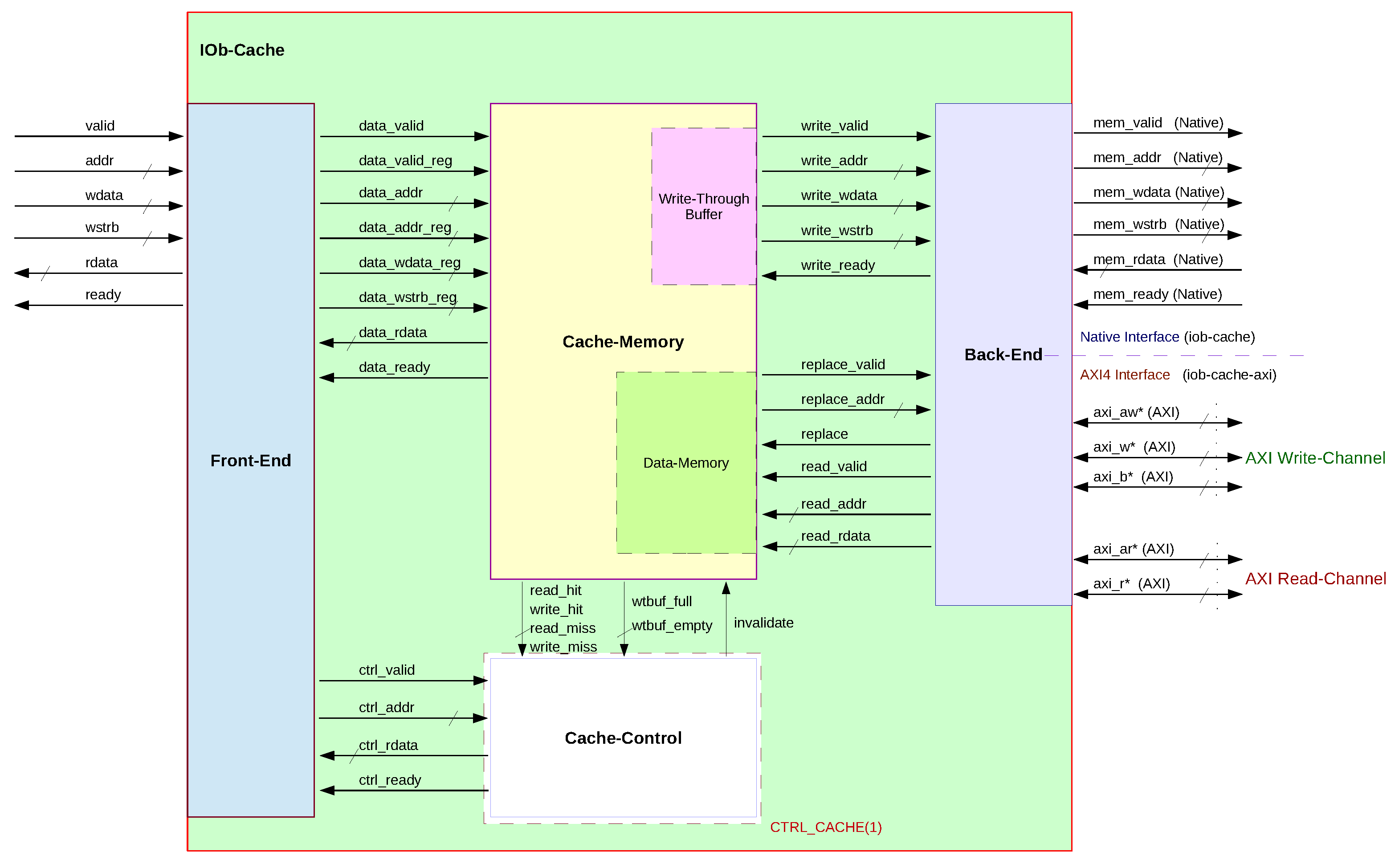
The top-level of the architecture integrates all the IOb-Cache modules (see Figure 1).
The Front-End connects the cache to a master processor. The ports always use the Native Interface, using a valid-ready protocol. The Back-End connects the cache (master) to the main-memory (slave). Its interface (Native or AXI) depends on the choice of the top-level module. The Cache-Memory is shown in between the Front-End and Back-End and contains all the cache memories and its main-controller. Cache-Control is an optional module for an L1 cache that allows performing tasks such as invalidating a data cache, requesting the status of its Write-Through Buffer, or analyzing its hit/miss performance.
2.2. Front-End
The Front-End module interfaces the processor (master) and the cache (slave). The current design splits the processor bus to access the cache memory itself or the Cache-Control module (if present). It also registers some bus signals needed by the cache memory. The prefix signals are sent to Cache-Memory, and the signals are sent to Cache-Control.
The cache always returns entire words since it is word-aligned. Therefore, the access is word-addressable, so the byte-offset of the CPU address signal (last bits) is not connected to the cache. In a system with a different CPU interface, only this module requires modification to allow compatibility. If the optional Cache-Control is implemented, this module also works as a memory-map decoder to select which unit is accessed.
2.3. Cache-Memory
Cache-Memory is a module that contains the cache controller and memories. The available memories are the Tag, the Valid, the Data, the Write-Through-Buffer, and, if applicable, the Replacement-Policy memory (see Figure 2).
The cache can be configured as direct-mapped or set-associative based on the number of ways given by parameter N_WAYS.
There is one Tag memory per cache way. Each of these has tag-sized width, and depth equal to the total number of cache lines. The Tag memory has one clock-cycle read latency. The Valid memory is composed of an array of 1-bit registers (register-file), one for each way. Each array length equals the number of cache lines. This choice of implementation is a simple design choice to set its contents to zero during either a system reset or a cache-invalidate.
The Data memory is implemented with one RAM for each way and (word) offset. Each RAM has a width FE_DATA_W (cache word-size) and a depth of (number of cache lines). Since the write-strobe signal selects which bytes are stored, each RAM requires a write enable for each byte. The Write-Though Buffer is implemented using a synchronous FIFO [16]. It requires the data to be available on its output a clock cycle after being read.
The input address signals are segmented as . The address is only used for the initial addressing (indexing) of the main memories: Valid, Tag, and Data. The stored address will be checked to see if a “cache hit” occurred to identify it within the cache line. Each of its bits indicates a hit in a separate way. The hit is the result of a tag match. If any bit of the “data_wstrb_reg” signal is enabled, it is a write-request; otherwise, it is a read-request.
If a read request produces a hit, the respective word is already available at the output of Data-Memory so that the request can be acknowledged.
The Data memory allows input data from both the Front-End and the Back-End. This selection is made using the signal , which indicates if the replacement on a cache line is in action. When is not asserted, all accesses are from the Front-End. During a read-miss, the signal is asserted, which will start the Back-End Read-Channel controller, responsible for line-replacement.
Both Tag and Valid memories are updated when the signal is high (read miss), forcing a hit in the selected way. Hence, the replacement process acts similarly to a regular write hit access. The replaced data () is validated () and positioned in the cache line (). This process depends on the size of the line and the back-end word-size. The replacement can only start if there are currently no write transfers to the main-memory.
The signals “write_valid” and “write_ready” constitute a handshaking pair for Cache-Memory to write to the Back-End Write-Channel. The former indicates that the Write-Through Buffer is not empty, validating the transfer. The latter indicates that the Back-End Write-Channel is idle and thus enables reading the Write-Through Buffer. The requirement that the replacement only starts after the write transfer is to avoid coherency issues.Write requests do not depend on the data being available in the cache, since it follows the write-not-allocate policy. Instead, it depends on the space available on the Writing-Through Buffer, which stores the address, write-data, and write-strobe array. During a write-hit, to avoid stalling, the Data memory uses the registered input signals to store the data so that the cache can receive a new request.
If a read-access follows a write-access, Read-After Write (RAW) hazards can become an issue. The requested word may not be available at the memory output, since it was written just the cycle before. This word will only be available in the following clock-cycle, therefore the cache needs to stall. Stalling on every read-request that follows a write hit-access can become costly performance-wise. Hence, to avoid this cost, a simple technique has been employed: the cache stalls only if one wants to read from the same way and word offset written before. Thus, the RAW hazard is only signaled when the same Data memory (byte-wide) RAMs are accessed.
2.4. Replacement Policy
The line replacement policy in a k-way set-associative cache is implemented by this module. Different available replacement policies can be selected using the “REP_POLICY” synthesis parameter. The module has three main components: the Policy Info Memory (PIM), the Policy Info Updater (PIU) datapath, and the Way Select Decoder (WSD).
The PIM stores information of the implemented policy. Note that replacement policies are dynamic and use data from the past, so memory is needed. The PIM has as many positions as the number of cache sets, addressed by the index part of the main memory address. The width of the PIM depends on the chosen policy. The PIM is implemented using a register-file so that during a system reset or cache invalidation, it can be set to default initial values.
When a cache hit is detected, the information stored in the PIM is updated based on the information previously stored for the respective set and the newly selected way. This function is performed by the PIU. When a cache miss is detected, the information for the respective cache set is read from the PIM and analyzed by the WSD to choose the way where the cache line will be replaced.
The currently implemented policies are the least-recently-used (LRU) and the pseudo-least-recently-used (tree and MRU-based).
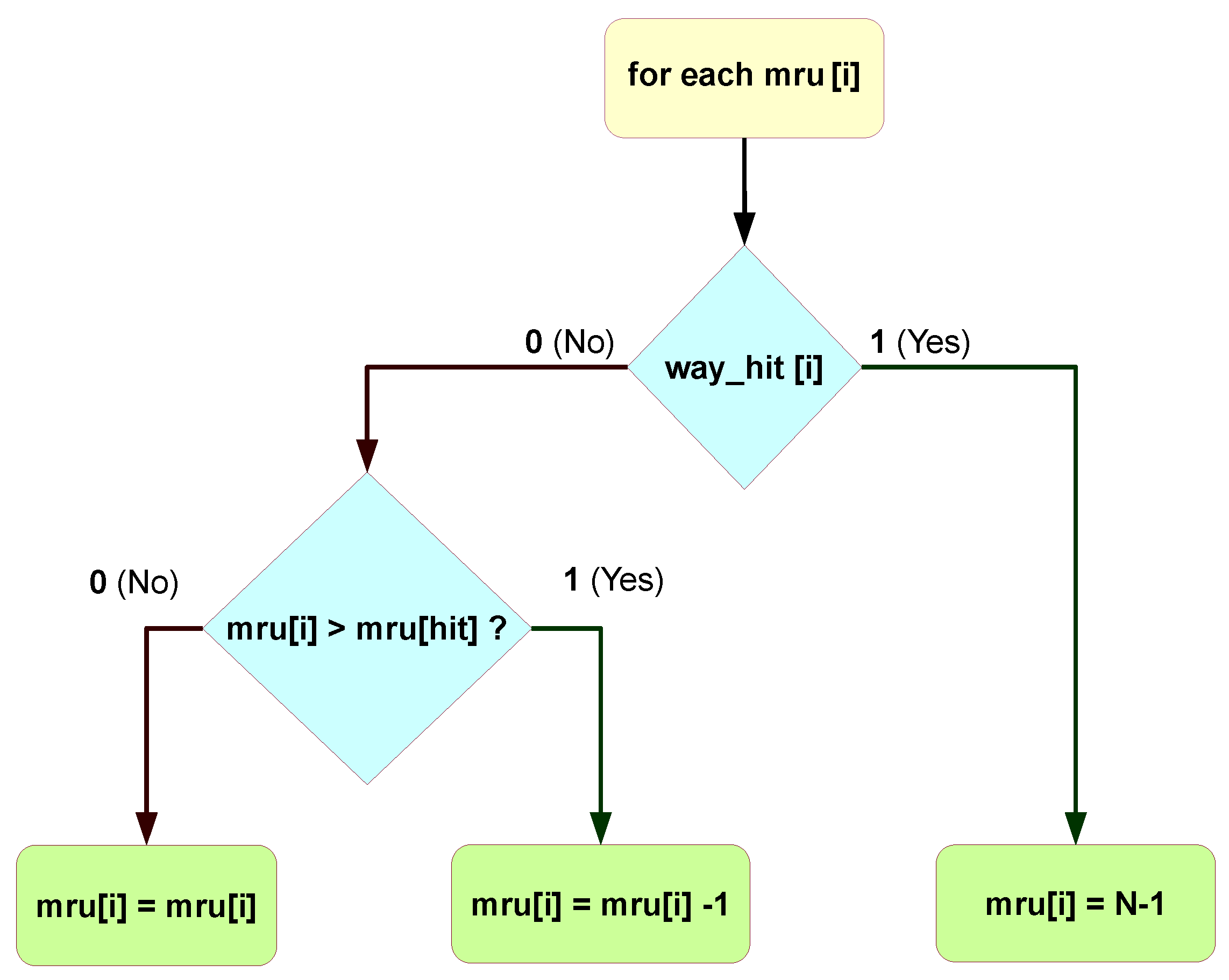
2.4.1. Least-Recently-Used
The LRU policy needs to store, for each set, a word that has N_WAYS fields of log2(N_WAYS) bits each. Each field, named “mru[i]”, represents how recently the way has been used by storing a number between 0 (least recently used) and N_WAYS-1 (most recently used), thus requiring (N_WAYS) bits. In total, it requires bits per cache set.
The way each mru[i] is updated is represented in Figure 3. Summarizing, when a way is accessed either by being hit or replaced, it becomes the most recently used and is assigned. The other ways with higher mru values than the accessed way get decremented. The ones with lower mru values are unchanged. The selected way for replacement is the one with the lowest “mru” index. This can be achieved by NORing each index, as implemented in Equation (1).
2.4.2. Pseudo-Least-Recently-Used: MRU-Based
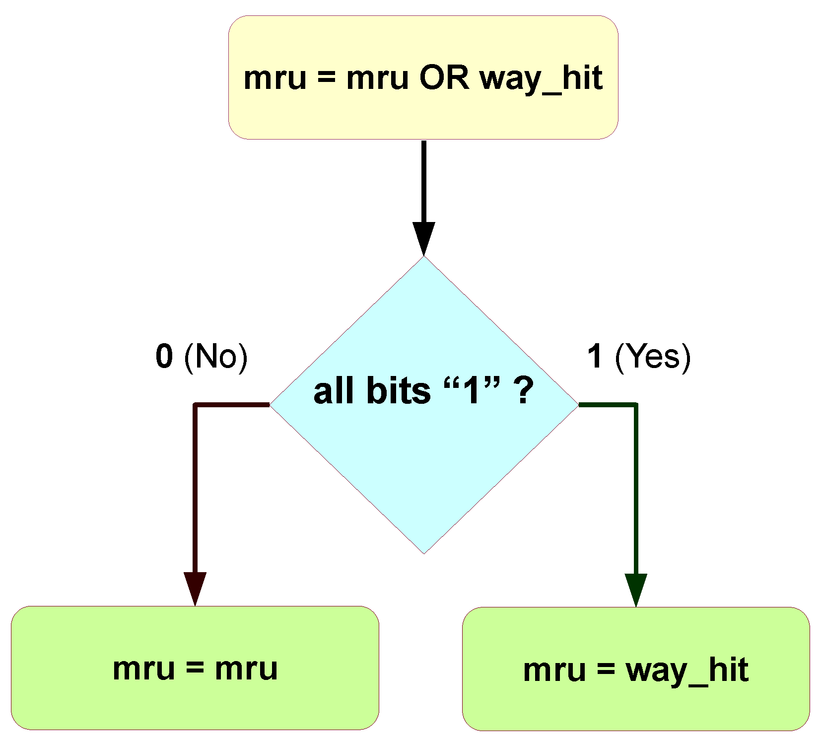
The PLRUm is simpler than the LRU replacement and needs to store, for each set, a word that has N_WAYS bits only. Each bit mru[i] represents how recently the way has been used, storing a 0 (least recently used) or 1 (most recently used), thus requiring (N_WAYS) bits.
The way each mru[i] is updated is represented in Figure 4. Summarizing, when a way is accessed either by being hit or replaced, the respective bit is assigned 1, meaning it has been recently used. When all ways have been recently used, the most recently assigned remains are asserted and the others are reset. This is done by simply ORing the way_hit signal and the stored bits, or storing the way_hit signal if all have been recently used. To select a way for replacement, the not recently used way (mru[i] = 0) with the lowest index is selected. This can be implemented by the following logic equation, Equation (2).
2.4.3. Pseudo-Least-Recently-Used: Binary Tree-Based
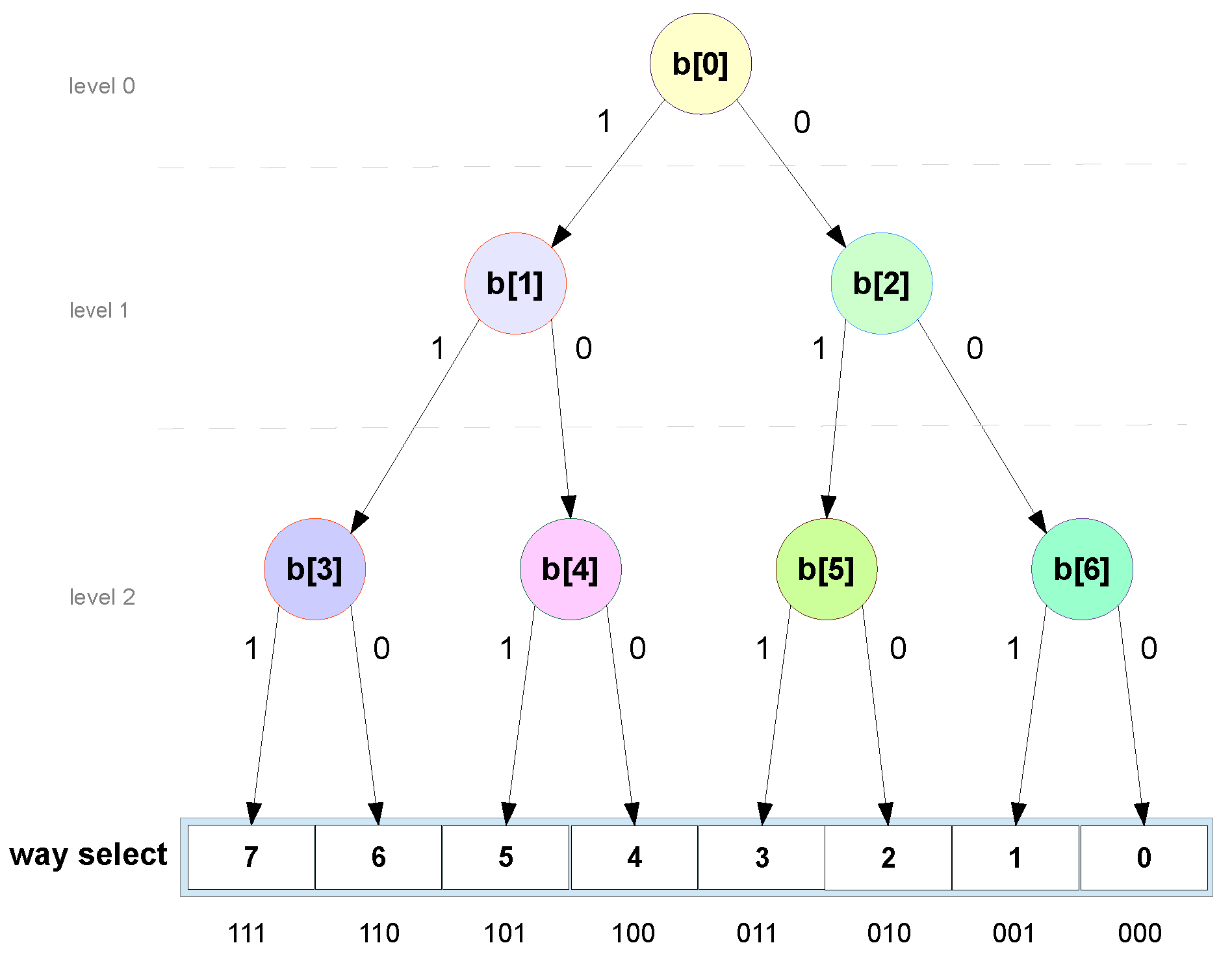
The PLRUt needs to store, for each set, a binary tree with levels and leaves, each representing a cache way. Each level divides the space to find the way in two, creating a path from the root node to the chosen way, when traversed by the WSD. Each node is represented by a bit b[i] where 0 selects the lower half and 1 selects the upper half of the space. For a 8-way example, the binary tree is represented in Figure 5.
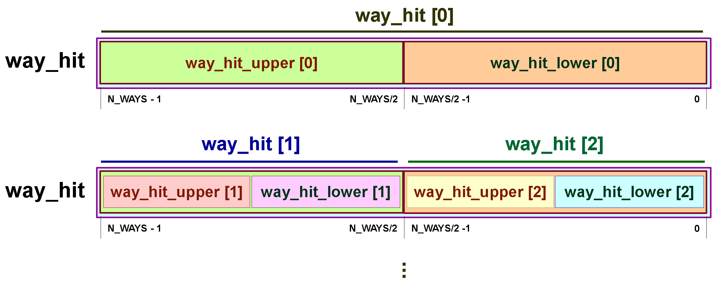
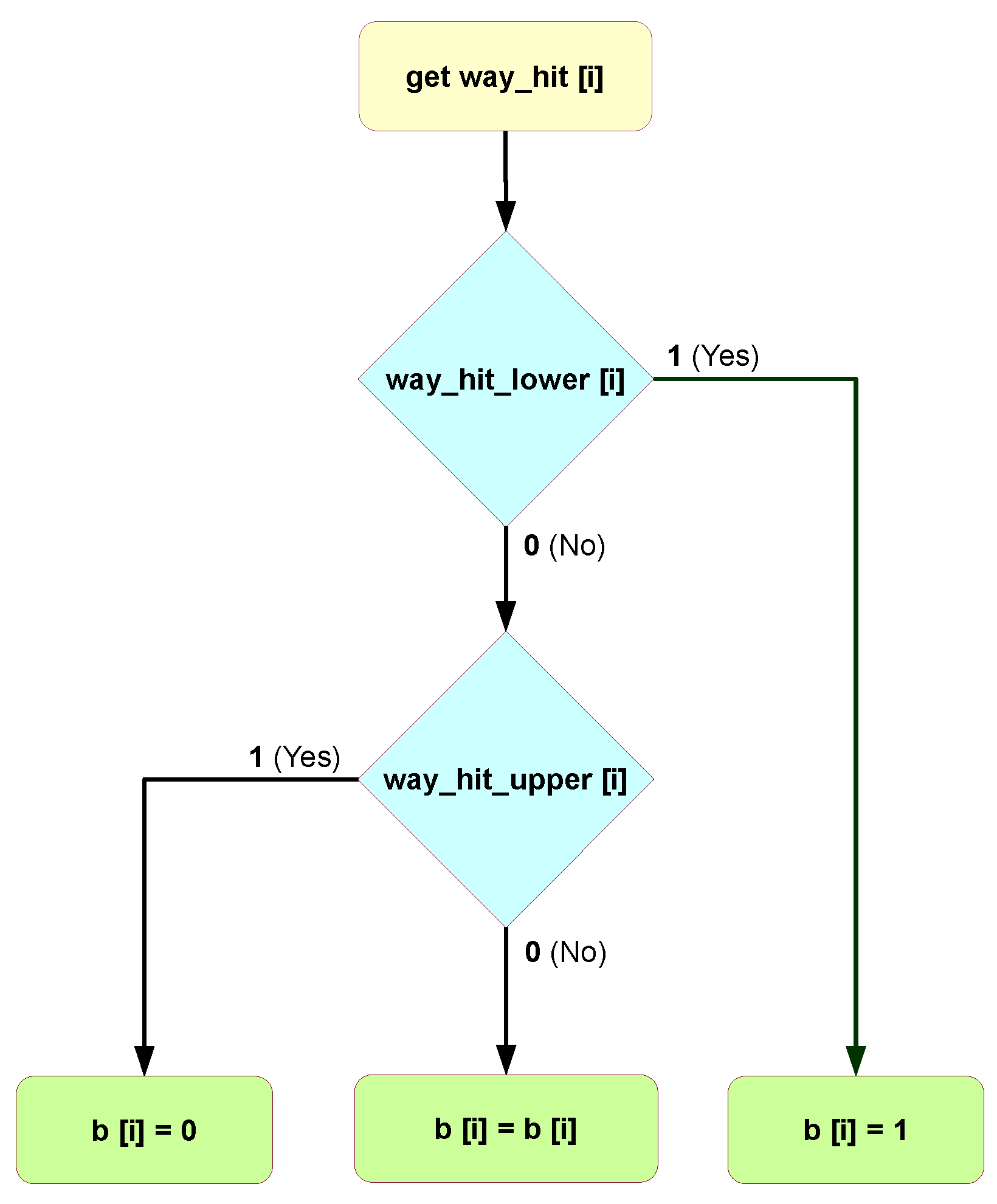
To update each node b[i], the first step is to get the slice way_hit[i] from the vector way_hit, relevant for computing b[i]. Figure 6 shows how to compute way_hit[i] for the first 3 notes, b[2:0]. After computing slice way_hit[i], the algorithm shown in Figure 7 is followed. The process is straightforward. If the slice is not hit (all its bits are 0), then b[i] remains unchanged. Otherwise, b[i] is set to 0 if the hit happens in the upper part of the slice and to 1 if the hit happens in the lower part.
To select the way for doing the replacement, the binary tree needs to be decoded. This can be done by iterating from the tree levels, from root to leaves, using the b[i] values to point to the next node until the leaf is reached. As explained before the leaf index is the chosen way.
2.5. Back-End
The Back-End module is the interface between the cache and the main memory. There are currently two available main memory interfaces: Native and AXI. The native interface follows a pipelined valid-ready protocol. The AXI interface implements the AXI4 protocol [17].
Although the AXI interface has independent write and read buses, the native interface only has a single bus available. In the native interface, the difference between a write and read access depends on the write-strobe signal (mem_wstrb) being active or not. This requires additional logic to select which controller accesses the main memory. There is no risk of conflict between the read and write channels: reading for line replacement can only occur after all pending writes are done.
The Back-End module has two controllers, the Write-Channel controller and the Read-Channel controller. The Write-Channel controller reads data from the Write-Through Buffer and writes data to the main memory while the buffer is not empty. The Read-Channel controller fetches lines from the main memory and writes them to the cache during a cache line replacement.
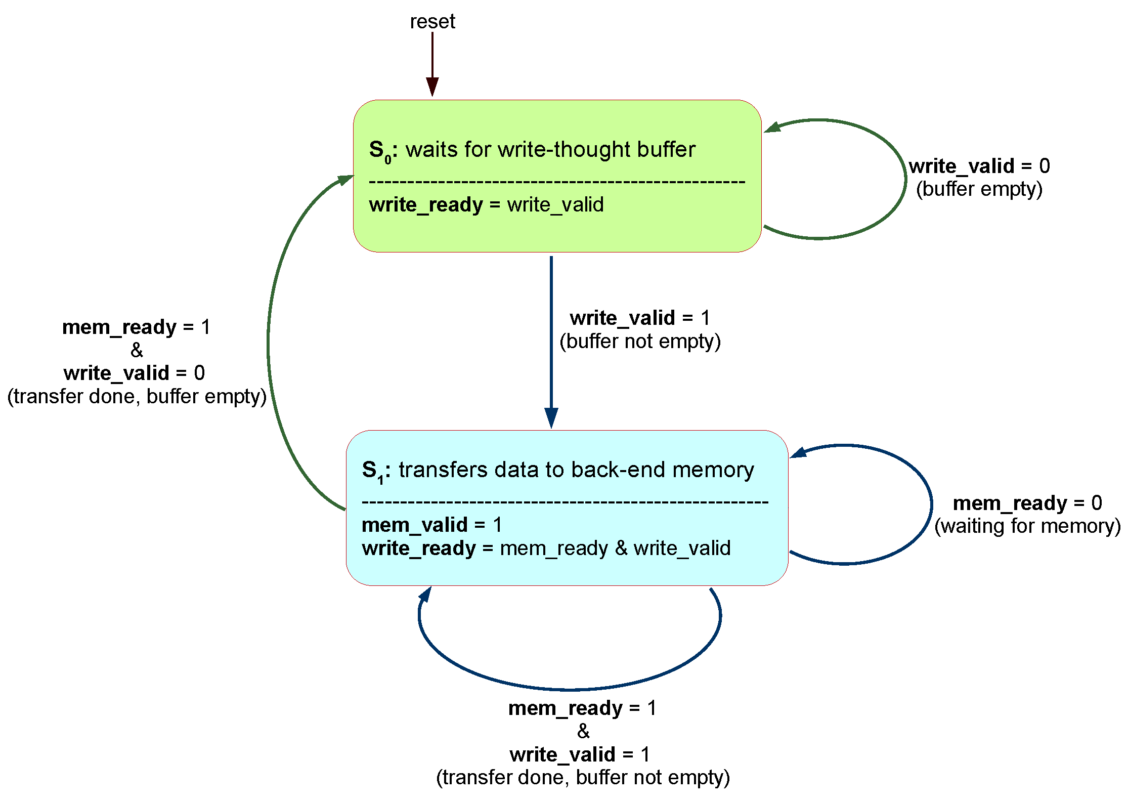
2.5.1. Write-Channel Controller
The controller of the native interface follows the control flow displayed in Figure 8. The controller stays in the initial state while waiting for the write-through buffer to have data. The write-through buffer uses a FIFO, and the FIFO starts the controller when it is not empty. When that happens, signal write_valid asserts, and the FIFO gets read.
In the following clock cycle, the required data is available in FIFO output and the transfer can occur. After each transfer, the FIFO is checked, and if it is not empty, it is read again so the data can be transferred in the following clock cycle. The process repeats until there are no more available data in the write-through buffer, and the controller goes back to its initial state.
The write-through buffer can only be read after each transfer is completed (mem_ready received). Currently, there is no way to pipeline these transfers, which are limited to one word per every two clock cycles. While the controller is in the initial state, the memory write-strobe signal is 0 to not disturb the Read-Channel controller.
The AXI-Interface has similar behavior but follows the AXI4 protocol. The address valid-read handshake needs to happen before any data can be transferred. After the data is transferred, it is checked to see if it was successful through the response channel (B channel): if axi_bresp does not have the OKAY value (an AXI code), then the transfer was unsuccessful and the data is transferred again.
If the Back-End data width (BE_DATA_W) is larger than the front-end (FE_DATA_W), the data buses require alignment. The address signal becomes word-aligned, discarding the back-end’s byte offset bits. These discarded bits are used to align both the write data and strobe.
This results in Narrow transfers [17], allowing the smaller words to be transferred to a larger bus. The Write-Channel data width is, therefore, limited to the cache front-end word-size. For example, in a 32-bit system, connected to a 256-bit wide memory, each transfer will be limited to 32-bit anyway.
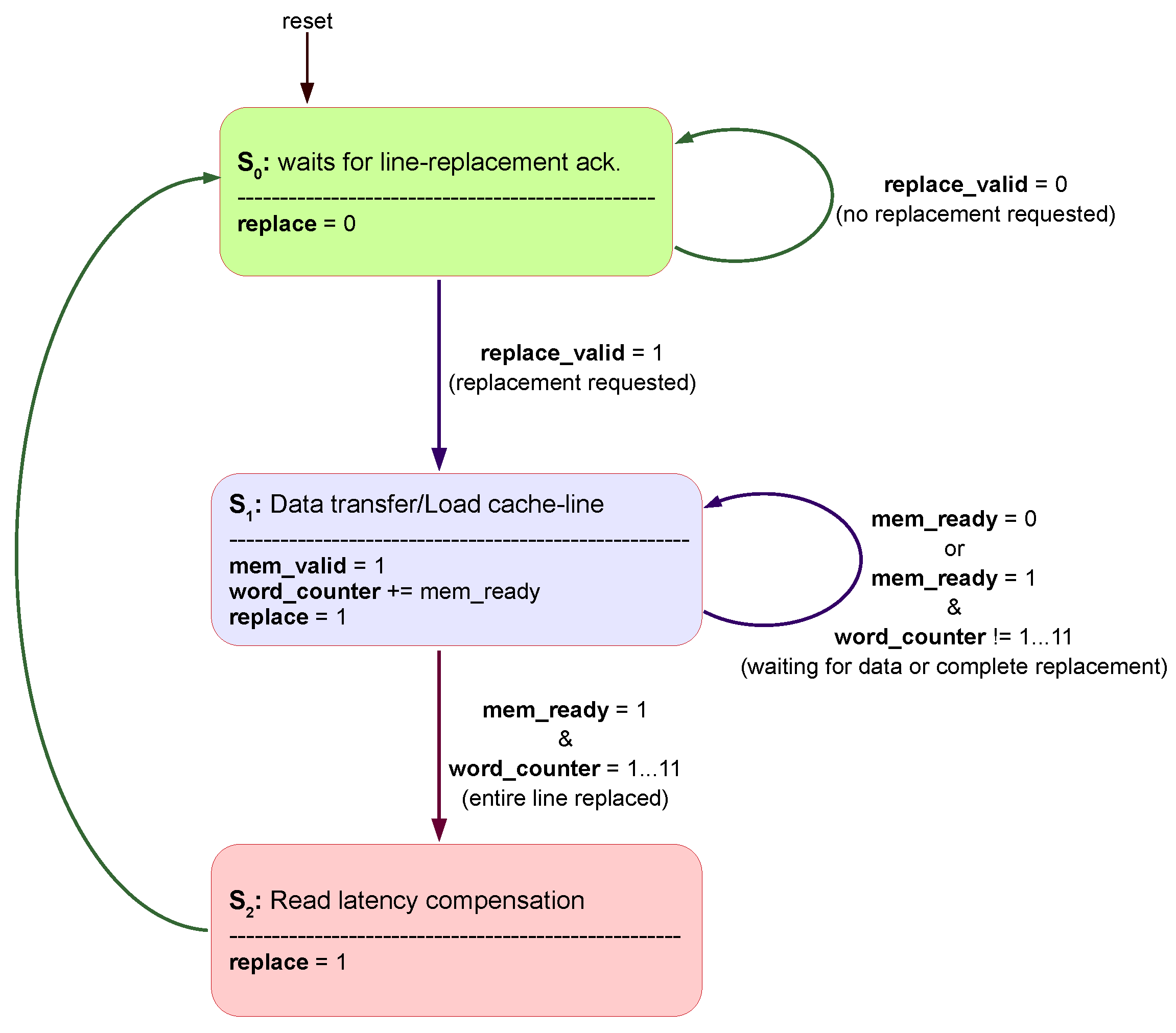
2.5.2. Read-Channel Controller
The controller of the native interface follows the control flow displayed in Figure 9. The controller stays in the initial state while waiting for the request of a line replacement. When signal “replace” is asserted, the controller goes to state requests a word block from the memory and writes it to the cache line at one word per cycle after it arrives at the back-end. It requests the base address of the main memory block and uses a word counter to count the received words. After the last word is received the controller goes to state for a single cycle to compensate for the memory read latency. Afterward, it goes back to its state , de-asserting signal “replace”.
If the back-end data width (BE_DATA_W) is multiple the front-end (FE_DATA_W), the number of words counted is proportionally shorter. If the back-end data width is the same size as the entire cache line, the burst length is one, and therefore the word counter is not used.
The AXI Interface controller has a similar behavior, but uses AXI4 burst transfers. The AXI burst parameters are derived for synthesis, using the front-end and back-end data widths, and the cache line offset width. Instead of using a word counter, the signal axi_rlast is used to know when the line has been fully replaced. During the burst, each beat (transfer) increments signal read_addr automatically.
Unlike the Write-Channel controller, the response signal, “axi_rresp”, is sent during each beat (transfer) of the burst. This requires the use of a register which sets in the case at least one of the beats was unsuccessful. After the transfers, the verification of this register can be done at the same time as the read latency compensation.
2.6. Cache-Control
The Cache-Control module can optionally be implemented using the synthesis parameter “CTRL_CACHE”. It is used to measure the cache performance, analyze the state of its write-through buffer, or invalidate its contents. Additionally, the parameter “CTRL_CNT” implements counters for cache hits and misses, for both read and write accesses.
The Cache-Control functions are controlled by memory-mapped registers, selected through . The addresses of the software accessible can be found in the cache’s Verilog and C header files.
The ports write_hit, write_miss, read_hit, and read_miss work as enables that cause the respective counters to increment. The counters can be reset by hardware (global system reset) or by software.
3. Results
This chapter presents results on IOb-Cache performance. A qualitative comparison between IOb-Cache and PoC.cache is also presented.
3.1. IOb-System-on-Chip
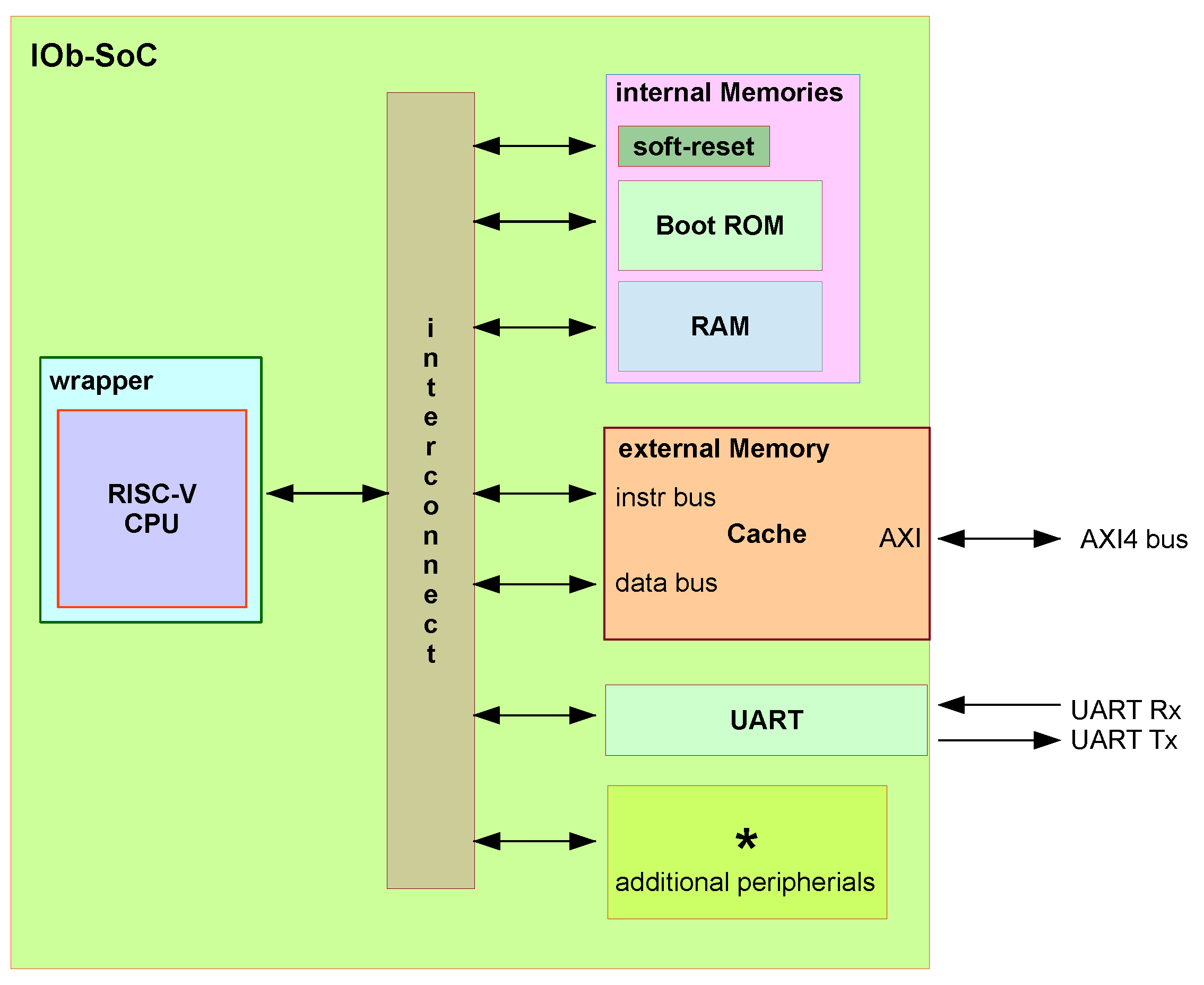
IOb-Cache has been integrated in IOb-SoC [18], an open-source synthesizable system developed by IObundle in Verilog. Its design can be seen in Figure 10.
The system is designed to allow the integration of multiple user peripherals, accessed through memory-mapping. Each individual peripheral device is given a specific address range to be accessed.
The interconnect is implemented with “split” [19] units, which is the module responsible for connecting the processor (master) to the remaining peripherals (slaves). The connection is established through memory-mapping, where the most significant bit (MSB) or the MSB-1 bit of the address selects all peripherals, depending on whether a secondary memory is present in the system.
This system is controlled by a RISC-V processor. A CPU wrapper converts the CPU interface signals to the Native interface used internally throughout the system for interconnecting the different modules. Currently, a simple 2-stage machine (PicoRV32 [20,21]), or a more complex super-scalar multi-issue processor (SSRV [22,23]) are supported.
For communications between the system and the host, a UART module (IOb-UART [24]) is integrated. It uses the universal asynchronous receiver/transmitter protocol (UART) for transmitting and receiving serial data.
A synchronous RAM (SRAM) memory and a boot read-only memory (ROM) are integrated into a module called Internal Memory, which also contains a soft reset mechanism for transitioning from the bootloader to the main program and vice-versa.
The External Memory module allows access to an external and larger DRAM memory (DDR3 or DDR4), and is where the IOb-Cache modules are placed. External Memory module connects the system to an external DDR memory soft controller provided by the FPGA vendor and using the AXI4 interface. This explains why AXI4 interfaces have been implemented for the cache back-end.
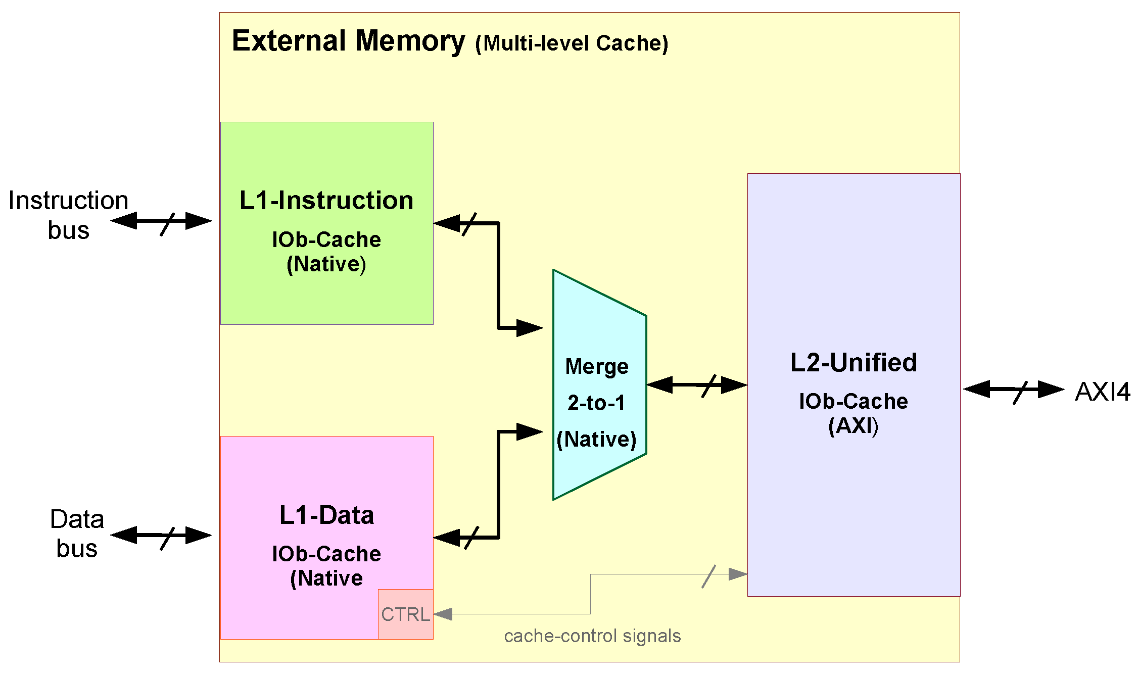
IOb-Cache modules can be connected to each other to form multi-level cache systems. A two-level cache system, composed of an L1-Instruction cache and an L1-Data cache, both connected to a larger L2-cache, is represented in Figure 11. The two L1 caches access different types of data, one accesses instructions, and the other accesses data. The L2 cache merges the accesses of the instruction and data caches and thus may contain both instructions and data.
The back-end of the L1 instruction and data caches use the Native Interface and are connected to a 2-to-1 interconnect called “merge” [19]. The merge unit connects several masters to a slave interface using a fixed and sequential priority encoder. A master remains connected to a slave until the request is acknowledged. The back-end of the merge block is connected to the front-end of the L2 cache which also uses the Native interface. The L2 back-end uses the AXI4 interface and is connected to the memory controller.
The Cache-Control optional module can only be implemented in the L1-Data cache since it is the only cache directly accessed by the processor, and the instruction L1 cache does not need one. To access the L2-cache, either for a cache invalidation or checking of the status of the write-through buffer, the CTRL_IO pins are used instead. The CRL_IO interface supports multi-cache systems, so accessing the Cache-Control module for status verification, shows the status of the downstream connected caches. This is necessary during the IOb-SoC booting procedure, to check if the entire firmware has already been written to the main memory before restarting the system to run it.
The IOb-SoC system has been implemented in an XCKU040-1FBVA676 FPGA [25], which is part of the Xilinx’s Ultrascale FPGA family.
3.2. Performance
The cache was evaluated with the Dhrystone [26] benchmark using the cycles per instruction (CPI) metric. The cache was initially simulated with different configurations and then tested in a field-programmable gate array (FPGA) device. The simulation results are displayed in Table 1, with the cache connected to an AXI4 RAM.
The minimum possible size for 2-level configuration is 48 Bytes, 16 Bytes for each of the three caches. This is the worst possible scenario performance-wise. If the L1 does not have the requested word, neither does the L2. The large delay in between instructions is caused by the high miss rate, causing accesses to the main memory, as well as traffic congestion between the L1 and L2 accesses.
Using 2 KB caches, one can see there is no performance difference between the replacement policies in a 2-way set-associative cache. The way selected is the one that was not the most recently used in all cases. It also shows the difference in performance between the set-associative and directly mapped cache. Using a set-associative in the L2-Unified cache represents the largest improvement in performance (up to 0.315 CPI). If the three caches only use direct mapping, the performance drops by 25.8%.
Using 4 KB caches highlights the differences in performance of the different replacement policies. The PLRUm policy displays the highest performance in all three caches, while the LRU policy gives the worst performance. The reduced size of the L1-Instruction (1 KB), and the firmware instruction loops constitute an environment where replacing the least recently used is not effective, due to low time locality. The PLRU policies lack memory compared to the LRU and are worse at identifying the most recently used line. However, this ends up not being a handicap as there is no time locality to exploit. The L2-Unified is more likely to see a performance improvement with PLRU policies [6,27]. This results from the fact L2 is accessing different memory blocks (instructions and data) with inherently low time locality.
Using 16 KB and 32 KB caches, the size is large enough to fit the program. There is no change in performance between the different replacement policies. Despite the program being 25 KB in size and the L1-Instruction caches 4 KB and 8 KB, respectively, the program is not required to fit entirely in these memories. As the program is executed, the only misses that occur are the initial compulsory misses, followed by capacity misses that replace the previous non-looping instructions. As the caches are big enough to store all recently looping code, conflict misses becoming nonexistent.
The real tests in FPGA are run in IOb-SoC [18], using the SSRV [22,23] multi-issue superscalar RISC-V processor. Despite being multi-issue, the processor was limited to one instruction per clock cycle in the tests, which is the optimal configuration for testing the cache. Connected to the IOb-SoC internal memory (RAM only and no cache), it achieved CPI = 1.02, running for 40445 clock cycles. The cache was implemented following a 2-level cache system: L1-Instruction and L1-Data caches connected to an L2-Unified cache (all implemented with IOb-Cache).
The FPGA system was implemented in the XCKU040 FPGA with a frequency of 50 MHz. Results with different cache sizes are presented in Table 2.
During the tests, some results were observed, such as in a 2-way set-associative cache, PLRUt is the best choice since it requires less stored bits while offering the same performance. Additionally, using a set-associative in the L2-Unified cache represents the most considerable performance improvement. The PLRUm policy displays the highest performance in all three caches, while the LRU policy gives the worst performance. This poor performance occurs because of the cache limited size.
3.3. Resources and Timing
In this section, the cache’s synthesis results are analyzed. First the resource utilization for different replacement policies is checked, followed by the resources consumed by the entire cache.
The synthesis tool used is Vivado Design Suite 2019 from Xilinx. Despite being able to change the cache’s word size with the parameter FE_DATA_W, it was left to 32-bit, since the cache was only tested in 32-bit systems.
The cache submodules are synthesized using a 100 MHz clock for the resources presented in the next subsections. The entire cache is synthesized at 100 and 250 MHz clock frequency and respective resources presented.
3.4. Replacement Policy
The Replacement Policy module is analyzed before the Cache-Memory module since the former is implemented in the latter. The results of the analysis are available in Table 3.
The test is divided into 2 sections: single cache line and multiple cache lines. It is not possible to synthesize the entire cache with a single cache line, so this is only valid for the analysis of this module.
The single cache line results show how many LUTs are required to implement the Policy Info Updater and Way Select Decoder. The number of FFs represents the number of bits the Policy Info Memory module needs to store for each set.
The multiple cache lines results show the current actual amount of resources required to implement each replacement policy. The current implementation of the Policy Info Module (PIM) is register-based, so it requires additional logic (LUTs) to address each set. The number of LUTs is proportional to the total number of bits in the PIM.
Since the LRU requires bits per set, initially its size grows fast with the number of ways. In an 8-way set-associative cache with 128 lines, the LRU requires more than twice the amount of LUTs and at least thrice the amount of FFs compared with the PLRU policies. In a 2-way set-associative cache, the replacement policies had the same performance, but the PLRUt’s PIM requires half the number of FFs compared to the other two.
3.5. Cache-Memory
Cache-Memory is the module that contains the majority of the cache’s resources. It contains all the RAM memories and, if configured, the Replacement Policy module too. The synthesis results are available in Table 4.
In the configurations with 128 lines or lower, the cache is implemented with LUTRAMs plus output registers. With 128 lines or more, RAMB18 is used. RAMB36 blocks are never inferred because these have a 36-bit width. The Write-Through Buffer, which is 64-bit wide, is implemented with LUTRAMs plus output registers if its depth is 32 or lower, or is implemented with RAMB36 if the depth is higher than 32. Note that RAMB36 blocks can be configured for 64-bit width and RAMB18 blocks can not.
In general, looking at the results in Table 4, the memory resources increase with both the width and depth of the cache memory. Increasing the number of ways, increases memory, and logic. The logic increases significantly to combine multiple ways and implement the Replacement Policy module.
3.6. IOb-Cache
Table 5 displays the synthesis and timing results of IOb-Cache using the Native interface for two different clock frequencies: 100 and 250 MHz. The results for IOb-Cache with AXI Back-End are similar and differ only in 15 LUTs and two FFs.
The implementation differs for the two clock frequencies. The used memory is enough for BRAMs to be inferred for both the Tag and Data memories. For 100 MHz, the critical-path is from Tag memory output to a Data memory write-enable signal.
For 250 MHz the synthesis tool implements the Tag-Memory with LUTRAMs, with a register at the output, to meet the timing constraint.
3.7. Open-Source Caches
The IOb-Cache was compared with the configurable PoC.cache design included in the PoC-Library [15] library of open-source cores. PoC.cache is the most competitive open-source cache one could find, so the other caches are not evaluated here; clearly, they cannot compete with IOb-Cache or PoC.cache. The comparison between the two caches is available in Table 6.
In addition to the information in Table 6, the following remarks are important. The PoC.cache back-end data-width is fixed to the cache line size, and therefore not configurable to be smaller such as in IOb-Cache.
The PoC.cache tag and valid memories are always implemented with distributed LUTRAM and registers, respectively, to combinatorially check for a hit and achieve one read per clock cycle. Lastly, despite using the Write-Though policy, PoC.cache does not have a buffer and accesses the main memory for write transfers, which is comparatively slower.
Based on the information in Table 6, there are two main points where PoC.cache is better than IOb-cache: (1) the cache invalidate function and (2) the support for a fully-associative cache. PoC.cache can invalidate individual lines, whereas IOb-Cache can only invalidate the entire cache. PoC.cache can be configured as fully associative (single set) cache and IOb-Cache needs at least two sets. However, besides its theoretical interest, fully associative caches are seldom used in practice.
In the remaining features, IOb-Cache is better than PoC.cache: configurable back-end size with AXI4 interface as an option; write-through buffer and independent controller for fast, most of the time one-cycle writing (PoC.cache only supports one clock cycle for reads); more replacement policies to choose from; a modular design that allows changing both front and back-ends without affecting the cache core functionality.
Both PoC.cache and IOb-cache have the same issue of implementing the Tag-Memory and Policy Info Module using registers, and thus consuming more silicon area than necessary. However, because IOb-Cache is designed to work with the one-cycle read latency of RAM, it can easily be upgraded to replace these memories with RAMs, while PoC.cache needs more drastic design changes.
4. Conclusions
In this paper, IOb-Cache, a high-performance configurable open-source cache was described. IOb-Cache is being used in dozens of projects. It is currently integrated into the IOb-SoC Github repository, which has 29 stars and is being used in 50 projects (forks). The Github cloud community is currently the only Verilog cache found by its search tool, with this level of configurability, that supports pipelined CPU architectures, and the popular AXI4 bus interface. Results running the cache integrated into a SoC show the proposed cache efficiency with a CPI of 1.06. This is possible because the proposed cache has a write-through buffer and an independent controller for fast 1-cycle writing.
Despite the promising results, there are some further improvements: (1) Implementation of the Write-Back Write-Allocate policy, the Write-Through policy limits the write-bus capacity to the cache word width. Ideally, these two policies should be configurable; (2) improve the Cache-Control module to allow invalidating of a single selected cache line; and (3) support for Cache Coherency for multi-processor systems.
Author Contributions
Conceptualization, J.V.R., J.D.L., M.P.V. and J.T.d.S.; Methodology, J.V.R., J.D.L., M.P.V. and J.T.d.S.; Software, J.V.R. and J.D.L.; Validation, M.P.V. and J.T.d.S.; Formal analysis, M.P.V. and J.T.d.S.; Investigation, J.V.R. and J.D.L.; Resources, M.P.V. and J.T.d.S.; Writing—original draft preparation, J.V.R.; Writing—review and editing, M.P.V. and J.T.d.S.; Supervision, J.T.d.S.; Project administration, J.T.d.S.; Funding acquisition, J.T.d.S. and M.P.V. All authors have read and agreed to the published version of the manuscript.
Funding
This work was supported by national funds through Fundação para a Ciência e a Tecnologia (FCT) with reference UIDB/50021/2020 and by the project PTDC/EEI-HAC/30848/2017, through INESC-ID.
Conflicts of Interest
The authors declare no conflict of interest.
References
- Akula, R.; Jain, K.; Kotecha, D.J. System Performance with varying L1 Instruction and Data Cache Sizes: An Empirical Analysis. arXiv 2019, arXiv:1911.11642. [Google Scholar]
- Ullah, Z.; Minallah, N.; Marwat, S.N.K.; Hafeez, A.; Fouzder, T. Performance Analysis of Cache Size and Set-Associativity using simpleScalar Benchmark. In Proceedings of the 2019 5th International Conference on Advances in Electrical Engineering (ICAEE), Dhaka, Bangladesh, 26–28 September 2019; pp. 440–447. [Google Scholar] [CrossRef]
- Ramasubramaniam, N.; Srinivas, V.V.; Kumar, P.P. Understanding the Impact of Cache Performance on Multi-core Architectures. In Information Technology and Mobile Communication; Das, V.V., Thomas, G., Lumban Gaol, F., Eds.; Springer: Berlin/Heidelberg, Germany, 2011; pp. 403–406. [Google Scholar]
- Ramasubramanian, N.; Srinivas, V.; Ammasai Gounden, N. Performance of Cache Memory Subsystems for Multicore Architectures. arXiv 2011, arXiv:1111.3056. [Google Scholar]
- Cantin, J.; Hill, M. Cache performance for selected SPECCPU2000 benchmarks. ACM Sigarch Comput. Archit. News 2001, 29, 13–18. [Google Scholar] [CrossRef]
- Al-Zoubi, H.; Milenkovic, A.; Milenkovic, M. Performance Evaluation of Cache Replacement Policies for the SPEC CPU2000 Benchmark Suite. In Proceedings of the 42nd Annual Southeast Regional Conference (ACM-SE 42), Huntsville, AL, USA, 2–3 April 2004; Association for Computing Machinery: New York, NY, USA, 2004; pp. 267–272. [Google Scholar] [CrossRef] [Green Version]
- Lentz, M.; Franklin, M. Performance of Private Cache Replacement Policies for Multicore Processors. In Proceedings of the 4th International Conference on Computer Science, Engineering and Applications, Dubai, United Arab Emirates, 7–8 March 2014; Volume 4, pp. 1–7. [Google Scholar] [CrossRef]
- Mirbagher Ajorpaz, S.; Garza, E.; Jindal, S.; Jiménez, D.A. Exploring Predictive Replacement Policies for Instruction Cache and Branch Target Buffer. In Proceedings of the 2018 ACM/IEEE 45th Annual International Symposium on Computer Architecture (ISCA), Los Angeles, CA, USA, 2–6 June 2018; pp. 519–532. [Google Scholar] [CrossRef]
- Stiliadis, D.; Varma, A. Selective victim caching: A method to improve the performance of direct-mapped caches. IEEE Trans. Comput. 1997, 46, 603–610. [Google Scholar] [CrossRef]
- Shukla, S.; Chaudhuri, M. Sharing-Aware Efficient Private Caching in Many-Core Server Processors. In Proceedings of the 2017 IEEE International Conference on Computer Design (ICCD), Boston, MA, USA, 5–8 November 2017; pp. 485–492. [Google Scholar] [CrossRef]
- Asaduzzaman, A.; Mahgoub, I.; Sibai, F.N. Evaluation of the impact of Miss Table and victim caches in parallel embedded systems. In Proceedings of the 2010 International Conference on Microelectronics, Cairo, Egypt, 19–22 December 2010; pp. 144–147. [Google Scholar] [CrossRef]
- Zhu, W.; Zeng, X. Decision Tree-Based Adaptive Reconfigurable Cache Scheme. Algorithms 2021, 14, 176. [Google Scholar] [CrossRef]
- airin711: Verilog Caches. 2016. Available online: https://github.com/airin711/Verilog-caches (accessed on 30 June 2021).
- prasadp4009: 2-Way-Set-Associative-Cache-Controller. 2016. Available online: https://github.com/prasadp4009/2-way-Set-Associative-Cache-Controller (accessed on 30 June 2021).
- PoC—Pile-of-Cores. Available online: https://github.com/VLSI-EDA/PoC (accessed on 30 June 2021).
- IOb-Memories. 2020. Available online: https://github.com/IObundle/iob-mem (accessed on 30 June 2021).
- AMBA AXI and ACE Protocol Specification. 2020. Available online: https://github.com/IObundle/iob-soc (accessed on 30 June 2021).
- IOb-SoC. 2020. Available online: https://github.com/IObundle/iob-soc (accessed on 30 June 2021).
- IOb-Interconnect. 2020. Available online: https://github.com/IObundle/iob-interconnect (accessed on 30 June 2021).
- Wolf, C. PicoRV32—A Size-Optimized RISC-V CPU. 2020. Available online: https://github.com/cliffordwolf/picorv32 (accessed on 30 June 2021).
- IOb-PicoRV32. Available online: https://github.com/IObundle/iob-picorv32 (accessed on 30 June 2021).
- Risclite. SuperScalar-RISCV-CPU. 2018. Available online: https://github.com/risclite/SuperScalar-RISCV-CPU (accessed on 30 June 2021).
- IOb-SSRV. 2020. Available online: https://github.com/IObundle/iob-ssrv (accessed on 30 June 2021).
- IOb-UART. 2020. Available online: https://github.com/IObundle/iob-uart (accessed on 30 June 2021).
- Avnet, Inc. Kintex UltraScale KU040 Development Board, Version 1.0. 2015. Available online: https://www.avnet.com/opasdata/d120001/medias/docus/13/aes-AES-KU040-DB-G-User-Guide.pdf (accessed on 20 July 2021).
- Weiss, A.R. Dhrystone Benchmark: History, Analysis, “Scores” and Recommendations, White Paper. 2002. Available online: https://www.eembc.org/techlit/datasheets/dhrystone_wp.pdf (accessed on 20 July 2021).
- Damien, G. Study of Different Cache Line Replacement Algorithms in Embedded Systems. Master’s Thesis, KHT—Royal Institute of Technology in Stockholm, Stockholm, Sweden, 2007. [Google Scholar]
Figure 1.
IOb-Cache top-level module diagram.

Figure 2.
Cache-Memory module diagram.

Figure 3.
LRU Encoder datapath flowchart.

Figure 4.
PLRUm Updater datapath flowchart.

Figure 5.
PLRU binary tree.

Figure 6.
Computing way_hit slices.

Figure 7.
PLRU way updater.

Figure 8.
Back-End write-channel native control-flow.

Figure 9.
Back-End read-channel native control-flow.

Figure 10.
IOb-SoC module diagram.

Figure 11.
External Memory: two-level cache system implementation.


Table 1.
Simulation Dhrystone SSRV (IOb-SoC) 32-bit. 100 runs using gcc -O1 optimization. Parameters: number of ways (repl. policy), lines, words per line.
Table 1.
Simulation Dhrystone SSRV (IOb-SoC) 32-bit. 100 runs using gcc -O1 optimization. Parameters: number of ways (repl. policy), lines, words per line.
| L1-Instr | L1-Data | L2-Unified | Clock Cycles | CPI |
|---|---|---|---|---|
| 48 B—Minimum size | ||||
| 1, 2, 2 | 1, 2, 2 | 1, 2, 2 | 319,580 | 8.066 |
| 2 KB | ||||
| 2 (LRU), 8, 8 | 2 (LRU), 8, 8 | 4 (PLRUm), 8, 8 | 162,147 | 4.092 |
| 2 (PLRUm), 8, 8 | 2 (PLRUm), 8, 8 | 4 (PLRUm), 8, 8 | 162,147 | 4.092 |
| 2 (PLRUt), 8, 8 | 2 (PLRUt), 8, 8 | 4 (PLRUm), 8, 8 | 162,147 | 4.092 |
| 1, 16, 8 | 1, 16, 8 | 4 (PLRUm), 8, 8 | 174,620 | 4.407 |
| 1, 16, 8 | 1, 16, 8 | 1, 16, 16 | 204,016 | 5.149 |
| 4 KB | ||||
| 4 (LRU), 8, 8 | 4 (LRU), 8, 8 | 8 (LRU), 8, 8 | 95,331 | 2.406 |
| 4 (LRU), 8, 8 | 4 (LRU), 8, 8 | 8 (PLRUm), 8, 8 | 87,031 | 2.196 |
| 4 (LRU), 8, 8 | 4 (LRU), 8, 8 | 8 (PLRUt), 8, 8 | 90,417 | 2.282 |
| 4 (PLRUm), 8, 8 | 4 (LRU), 8, 8 | 8 (PLRUm), 8, 8 | 79,310 | 2.001 |
| 4 (PLRUt), 8, 8 | 4 (LRU), 8, 8 | 8 (PLRUm), 8, 8 | 84,854 | 2.141 |
| 4 (PLRUm), 8, 8 | 4 (PLRUm), 8, 8 | 8 (PLRUm), 8, 8 | 79,310 | 2.001 |
| 4 (PLRUm), 8, 8 | 4 (PLRUt), 8, 8 | 8 (PLRUm), 8, 8 | 79,310 | 2.001 |
| 1, 64, 4 | 1, 64, 4 | 1, 64, 8 | 107,668 | 2.717 |
| 8 KB | ||||
| 2, 16, 16 | 2, 16, 16 | 4 (LRU), 16, 16 | 50,758 | 1.281 |
| 2, 16, 16 | 2, 16, 16 | 4 (PLRUm), 16, 16 | 50,751 | 1.281 |
| 2, 16, 16 | 2, 16, 16 | 4 (PLRUt), 16, 16 | 50,758 | 1.281 |
| 1, 32, 16 | 1, 32, 16 | 1, 64, 16 | 77,306 | 1.951 |
| 1, 64, 8 | 1, 64, 8 | 1, 128, 8 | 71,543 | 1.805 |
| 16 KB | ||||
| 4, 16, 16 | 4, 16, 16 | 8, 16, 16 | 41,837 | 1.055 |
| 4, 32, 8 | 4, 32, 8 | 8, 32, 8 | 41,762 | 1.055 |
| 2, 64, 8 | 2, 64, 8 | 4, 64, 8 | 41,886 | 1.057 |
| 1, 64,16 | 1, 64, 16 | 1, 128, 16 | 56,848 | 1.434 |
| 1, 128, 8 | 1, 128, 8 | 1, 128, 16 | 54,986 | 1.387 |
| 32 KB | ||||
| 8, 16, 16 | 8, 16, 16 | 16, 16, 16 | 41,837 | 1.055 |
| 2, 128, 8 | 2, 128, 8 | 4, 128, 8 | 41,762 | 1.054 |
| 1, 256, 8 | 1, 256, 8 | 1, 256, 16 | 41,811 | 1.055 |
| 2, 64, 16 | 2, 64, 16 | 4, 64, 16 | 41,837 | 1.055 |
Table 2.
FPGA emulation of Dhrystone SSRV (IOb-SoC) 32-bit at 50 MHz. 100 runs. 2-level cache system, sizes are for L1-Instr + L1-Data + L2-Unified.
Table 2.
FPGA emulation of Dhrystone SSRV (IOb-SoC) 32-bit at 50 MHz. 100 runs. 2-level cache system, sizes are for L1-Instr + L1-Data + L2-Unified.
| Cache Size (L1 + L1 + L2) | Clock Cycles | CPI |
|---|---|---|
| no cache | 594,345 | 15.017 |
| 48 B (16 + 16 + 16) | 513,926 | 12.971 |
| 2 KB (0.5 + 0.5 + 1) | 185,163 | 4.673 |
| 8 KB (2 + 2 + 4) | 51,298 | 1.294 |
| 32 KB (8 + 8 + 16) | 42,397 | 1.070 |
Table 3.
Replacement Policy resources.
| R.Policy | Ways | Lines | LUT | FF |
|---|---|---|---|---|
| Single cache line | ||||
| LRU | 2 | 1 | 3 | 2 |
| PLRUm | 2 | 1 | 3 | 2 |
| PLRUt | 2 | 1 | 3 | 1 |
| LRU | 4 | 1 | 20 | 8 |
| PLRUm | 4 | 1 | 8 | 4 |
| PLRUt | 4 | 1 | 6 | 3 |
| LRU | 8 | 1 | 81 | 24 |
| PLRUm | 8 | 1 | 22 | 8 |
| PLRUt | 8 | 1 | 13 | 7 |
| Multiple cache lines | ||||
| LRU | 2 | 16 | 26 | 32 |
| PLRUm | 2 | 16 | 26 | 32 |
| PLRUt | 2 | 16 | 28 | 16 |
| LRU | 4 | 16 | 70 | 128 |
| PLRUm | 4 | 16 | 42 | 64 |
| PLRUt | 4 | 16 | 33 | 48 |
| LRU | 8 | 16 | 196 | 384 |
| PLRUm | 8 | 16 | 77 | 128 |
| PLRUt | 8 | 16 | 56 | 112 |
| LRU | 2 | 128 | 343 | 512 |
| PLRUm | 2 | 128 | 222 | 256 |
| PLRUt | 2 | 128 | 212 | 128 |
| LRU | 4 | 128 | 445 | 1024 |
| PLRUm | 4 | 128 | 297 | 512 |
| PLRUt | 4 | 128 | 259 | 384 |
| LRU | 8 | 128 | 1076 | 3072 |
| PLRUm | 8 | 128 | 452 | 1024 |
| PLRUt | 8 | 128 | 403 | 896 |
Table 4.
Cache-Memory resources.
| Ways | R.Policy | Lines | Words/Line | LUT | LUTRAM | FF | RAMB36 | RAMB18 |
|---|---|---|---|---|---|---|---|---|
| 1 KB | ||||||||
| 1 | 16 | 16 | 496 | 534 | 599 | 1 | 0 | |
| 1 | 64 | 4 | 292 | 128 | 239 | 1 | 1 | |
| 1 | 128 | 2 | 300 | 0 | 174 | 1 | 9 | |
| 2 KB | ||||||||
| 1 | 32 | 16 | 548 | 533 | 614 | 1 | 0 | |
| 1 | 128 | 4 | 341 | 0 | 175 | 1 | 17 | |
| 2 | PLRUt | 16 | 16 | 950 | 1068 | 1167 | 1 | 0 |
| 4 KB | ||||||||
| 1 | 32 | 32 | 995 | 1044 | 1126 | 1 | 0 | |
| 1 | 128 | 8 | 405 | 0 | 176 | 1 | 33 | |
| 2 | PLRUt | 128 | 4 | 819 | 0 | 433 | 1 | 34 |
| 8 KB | ||||||||
| 1 | 128 | 16 | 551 | 0 | 177 | 1 | 65 | |
| 2 | LRU | 128 | 8 | 1037 | 0 | 562 | 1 | 66 |
| 2 | PLRUm | 128 | 8 | 1037 | 0 | 562 | 1 | 66 |
| 2 | PLRUt | 128 | 8 | 1003 | 0 | 434 | 1 | 66 |
| 16 KB | ||||||||
| 1 | 128 | 32 | 957 | 0 | 178 | 1 | 129 | |
| 1 | 512 | 8 | 933 | 0 | 560 | 1 | 33 | |
| 4 | LRU | 128 | 8 | 2055 | 0 | 1590 | 1 | 132 |
| 4 | PLRUm | 128 | 8 | 1913 | 0 | 1078 | 1 | 132 |
| 4 | PLRUt | 128 | 8 | 1877 | 0 | 950 | 1 | 132 |
| 4 | PLRUt | 64 | 16 | 2282 | 0 | 1845 | 1 | 68 |
| 32 KB | ||||||||
| 1 | 128 | 64 | 1760 | 0 | 179 | 1 | 257 | |
| 1 | 1024 | 8 | 1616 | 0 | 1072 | 1 | 33 | |
| 8 | LRU | 128 | 8 | 3935 | 0 | 4158 | 1 | 264 |
| 8 | PLRUm | 128 | 8 | 3341 | 0 | 2110 | 1 | 264 |
| 8 | PLRUt | 128 | 8 | 3293 | 0 | 1982 | 1 | 264 |
Table 5.
IOb-Cache (Native) resource and timing analysis.
| Ways | R.Policy | Lines | Words/Line | LUT | LUTRAM | FF | RAMB36 | RAMB18 |
|---|---|---|---|---|---|---|---|---|
| 100 MHz (10 ns) | ||||||||
| 4 KB | ||||||||
| 1 | 128 | 8 | 431 | 0 | 249 | 1 | 33 | |
| 4 | PLRUm | 16 | 16 | 1727 | 1068 | 2407 | 1 | 0 |
| 8 KB | ||||||||
| 2 | PLRUt | 128 | 8 | 1025 | 0 | 509 | 1 | 66 |
| 16 KB | ||||||||
| 4 | PLRUm | 128 | 8 | 1940 | 0 | 1154 | 1 | 132 |
| 32 KB | ||||||||
| 4 | PLRUm | 256 | 8 | 2961 | 0 | 2187 | 1 | 132 |
| 1 | 1024 | 8 | 1638 | 0 | 1145 | 1 | 33 | |
| 250 MHz (4 ns) | ||||||||
| 4 KB | ||||||||
| 1 | 128 | 8 | 510 | 40 | 269 | 1 | 32 | |
| 4 | PLRUm | 16 | 16 | 1730 | 1068 | 2407 | 1 | 0 |
| 8 KB | ||||||||
| 2 | PLRUt | 128 | 8 | 1084 | 80 | 549 | 1 | 64 |
| 16 KB | ||||||||
| 4 | PLRUm | 128 | 8 | 1974 | 160 | 1234 | 1 | 128 |
| 32 KB | ||||||||
| 1 | 1024 | 8 | 1714 | 272 | 1162 | 1 | 32 | |
| 4 | PLRUm | 256 | 8 | 2981 | 304 | 2289 | 1 | 128 |
Table 6.
Comparison between PoC.cache and IOb-Cache.
| PoC.Cache [15] | IOb-Cache | |
|---|---|---|
| HDL | VHDL | Verilog |
| Configurability | ||
| n. ways, lines, words | Yes | Yes |
| back-end width | No | Yes |
| Mapping | ||
| Direct | Yes | Yes |
| Set-Assoc. | Yes | Yes |
| Full-Assoc. | Yes | No |
| Policies | ||
| Write | write-through | write-through |
| W.T. Buffer | No | Yes |
| Replacement | LRU | LRU, PLRUs |
| Back-End Connectivity | ||
| Native | Yes | Yes |
| AXI | No | AXI4 |
| Implementation | ||
| Main-control | FSM | Data-path |
| Data-Memory | BRAM | BRAM |
| Tag-Memory | LUTRAM | BRAM |
| Valid-Memory | Register | Register |
| Rep-Pol. Mem | Register | Register |
| Invalidate | Yes | Yes |
| Performance | ||
| clk/read (hit) | 1 | 1 |
| clk/write | 2 | 1 |
| Ready | during valid | after valid req. |
| Read-Data avail. | after ready | during ready |
| New req. | after ready | during ready |
Publisher’s Note: MDPI stays neutral with regard to jurisdictional claims in published maps and institutional affiliations. |
© 2021 by the authors. Licensee MDPI, Basel, Switzerland. This article is an open access article distributed under the terms and conditions of the Creative Commons Attribution (CC BY) license (https://creativecommons.org/licenses/by/4.0/).
Share and Cite
MDPI and ACS Style
Roque, J.V.; Lopes, J.D.; Véstias, M.P.; de Sousa, J.T. IOb-Cache: A High-Performance Configurable Open-Source Cache. Algorithms 2021, 14, 218. https://0-doi-org.brum.beds.ac.uk/10.3390/a14080218
AMA Style
Roque JV, Lopes JD, Véstias MP, de Sousa JT. IOb-Cache: A High-Performance Configurable Open-Source Cache. Algorithms. 2021; 14(8):218. https://0-doi-org.brum.beds.ac.uk/10.3390/a14080218
Chicago/Turabian StyleRoque, João V., João D. Lopes, Mário P. Véstias, and José T. de Sousa. 2021. "IOb-Cache: A High-Performance Configurable Open-Source Cache" Algorithms 14, no. 8: 218. https://0-doi-org.brum.beds.ac.uk/10.3390/a14080218
Note that from the first issue of 2016, this journal uses article numbers instead of page numbers. See further details here.