Article

A High Gain AC-DC Rectifier Based on Current-Fed Cockcroft-Walton Voltage Multiplier for Motor Drive Applications

by
Ahmad Zarepour
1,
Amirhossein Rajaei
1,*,
Hooman Mohammadi-Moghadam
1 and
Mahdi Shahparasti
2
1
Department of Electrical Engineering, Shiraz University of Technology, Shiraz 71557-13876, Iran
2
Flexible Energy Resources, School of Technology and Innovations, University of Vaasa, 65200 Vaasa, Finland
*
Author to whom correspondence should be addressed.
Sustainability 2021, 13(21), 12317; https://0-doi-org.brum.beds.ac.uk/10.3390/su132112317
Submission received: 26 August 2021 / Revised: 31 October 2021 / Accepted: 4 November 2021 / Published: 8 November 2021

Abstract

:
This paper proposes a novel high-gain AC-DC converter based on the Cockcroft-Walton (CW) voltage multiplier which can be utilized in motor drive systems with low input voltage. In this topology, use of the voltage multiplier and boost circuit results in the increment of converter gain which has a significant impact on the cost and efficiency of the system. Moreover, in this converter, the AC voltage is directly changed to DC voltage using the switching method in high frequency and, as well, the power factor is corrected. Besides, this high-frequency converter contributes to the reduction of output ripple. On the other hand, cost efficiency, the low voltage stress on capacitors and diodes, compactness, and the high voltage ratio, are achieved from the Cockcroft-Walton circuit. Furthermore, the hysteresis method is presented for converter switching to correct the power factor. The converter is simulated in MATLAB software to demonstrate the effectiveness of the suggested method. Lastly, a laboratory prototype of the suggested converter is built, several tests are done in order to verify the theoretical analysis, and comprehensive comparison with the state-of-the-art converter is done.

1. Introduction

Nowadays, high gain AC/DC converters are widely used in manufacturing, research, medicine, and the military, such as laboratory devices, X-ray facilities, dust screening, insulation inspection, and electrostatic coating [1,2,3,4]. In other applications, such as a motor drive, the system consists of an inverter for controlling the motor and a typical type of rectifier for changing the AC to DC voltage. In addition, in this structure, the DC voltage must be higher than 1.63 times the motor voltage; therefore, a high gain rectifier must be used to boost the AC input voltage in case of feeding through a low voltage source. Sustainable renewable energy sources are new energy systems that are widely used to meet the growing energy needs of today and tomorrow. In order to use the variable generated power by renewable power plants, employing a high-performance interface system is inevitable. As an example, the interface system for a wind energy power plant includes two parts:
  • • Generator: generates electric power from mechanical energy. Several types of generators such as induction, synchronous, and permanent magnet (PM) generators are used;
  • • Power interface system: regulates voltage and current and transfers energy from generator to the power grid or standalone load.
Due to the low output voltage of generators and most other renewable energy systems, high step-up converters are widely used as a part of interface systems to achieve better performance and higher efficiency. In this paper, we have introduced a new structure of an AC-DC high step-up converter which can be used as a power electronic interface for renewable energy systems.
Traditional converters such as current source converter (CSC) and voltage source converter (VSC), which are normally used in most industries, have several disadvantages. Disadvantages are that (1) the main switching component of VSC and CSC are not interchangeable, (2) they operate as a boost or buck converter only, (3) to have a multi-functional DC/AC converter, a DC-DC converter and VSC must be combined which leads to lower reliability, and (4) being exposed to the EMI phenomenon and the components in either short or open circuit mode causes detriment. Therefore, the range of output voltage is restricted in comparison to the input voltage. In addition, Z-source inverters include the whole range of power conversion applications, and they have some benefits, such as removing switches which are normally needed at the boosting point for increasing stability due to not being sensitive to shoot-through. Although, they usually involve higher voltage level switches [5]. In [6,7,8,9], researchers have thoroughly studied DC-DC converters with high turn ratio transformers that are isolated. While they have galvanic insulation that is critical for many applications, their disadvantages are their large parasite efficiency and high-turn-ratio transformer leakage inductance, which induces high current spikes and high voltage on semi-conductor components. Because of its essential property, the Switched-Capacitor Converter has drawn attention because it requires no magnetic part contribution [10,11]. Compared with conventional inductor-based converters, this feature allows it to achieve higher power density and complete monolithic mixture [12,13,14]. The important disadvantage is that it carries restricted control capacity and pulsating feedback current, which is cause for concern [15].
The controllable output AC-DC converters are employed for use in DC-AC and DC-DC converters. Because of severe regulation on conducted electromagnetic interference, passive and active power factor correction is required [16]. Multiple switches in inverter systems are often employed in bi-directional power flow, among different PWM rectifications. Such converters exhibit appropriate output regarding the total harmonic distortion of input current, efficiency, and power factor due to the pulse width modulation function. Multiple PWM rectifiers involve a complicated controller and require safety against the failure of switching equipment [17]. Also, the harmonic current injection approach is employed in large three-phase rectifier systems for power factor enhancement and correction of input current. Harmonic injection strategies involve the injection of a different or related DC source to produce a harmonic current, and also in order to alter the duty cycle of the rectifier switch, and a suitable voltage is used in the control procedure [18,19]. The suitable input filter reduces the converter’s performance. Regarding this, Vienna rectifiers are common converters, in which three switches control current waveforms at the input side. Vienna rectifiers are studied with their initial and updated topologies, and, as well, a closed-loop Vienna rectifier has been observed providing reasonable output with boost voltage gain [20,21,22,23,24,25,26,27,28,29]. The traditional rectifiers are durable and inexpensive; however, they draw reactive power or non-sinusoidal currents from the source, which reduces the efficiency of the component. Power factor correction (PFC) or passive linear filters topologies may be utilized to counteract harmonic distortion caused by regular rectifiers [30,31,32]. The three-phase multi-pulse rectifiers gain harmonic cancellation by the addition of a three-phase transformer using phase shift. In fact, the diode rectifier’s simplicity and durability characteristics are retained; although, they are heavy, voluminous, and costly [33,34]. Benefiting from high-frequency switching technology, several improved CW circuits have been developed to save transformer volume, as well as controlling the output voltage and reducing output ripple. Voltage-fed modified CW topologies were proposed in [35,36,37], which prepare ease of implementation as well as a high voltage gain. However, in such structures, the high-frequency transformer with lower turn ratios induces the inductance of leakage and large winding efficiency, resulting in higher switching losses on the switch and heavy current and voltage pressures. The key problems associated with CW-VM are the current-dependent voltage drop and the voltage ripple, which can deteriorate converter output, particularly for those with a large number of stages. To solve these issues, a variety of improvements have been suggested, such as the use of a current-fed system [38,39]. In addition, the current-fed Capacitor diode voltage multipliers (CD-VM) system is a viable alternative that might be employed for the boosting stage of low-voltage renewable energy capital control electronic interface. Among different forms of CD-VM, the most common circuit is half-wave (CW-VM) [40,41]. The standard Cockcroft-Walton (CW) voltage multiplier offers the benefits of cost-efficiency, a low voltage stress on capacitors and diodes, and a high voltage ratio. A CW voltage multiplier is designed in every stage using cascading multiple diode-capacitor stages that have two diodes and two capacitors. Further, ref. [42] presents an analytical design procedure for RF energy harvesting systems using the CWVM structure. As well, ref. [43] analyzed the operation principles of an n-stage current-fed Cockcroft-Walton (CF-CWVM) during transient and steady-state operations. The derived relations can be used for further explanation of the converter behaviour as well as a non-linear controller design. A design of high-voltage multipliers to generate underwater shockwaves is also described in [44].
In this article, a novel high-step current-fed rectifier has been introduced that uses a current-fed CW-VM, and also has two inductors and four switches. The low voltage tension on the switches allows low voltage MOSFETs to be used to increase both performance and reliability. Moreover, this article has been organized as follows. In Section 2, the steady-state analysis is presented. Section 3 discusses design considerations of the converter, and its control system is presented in Section 4. In Section 5, the simulation and experimental results that allowed us to validate the performance of the proposed converter are presented. Lastly, the conclusions of the proposed work are demonstrated in Section 6.

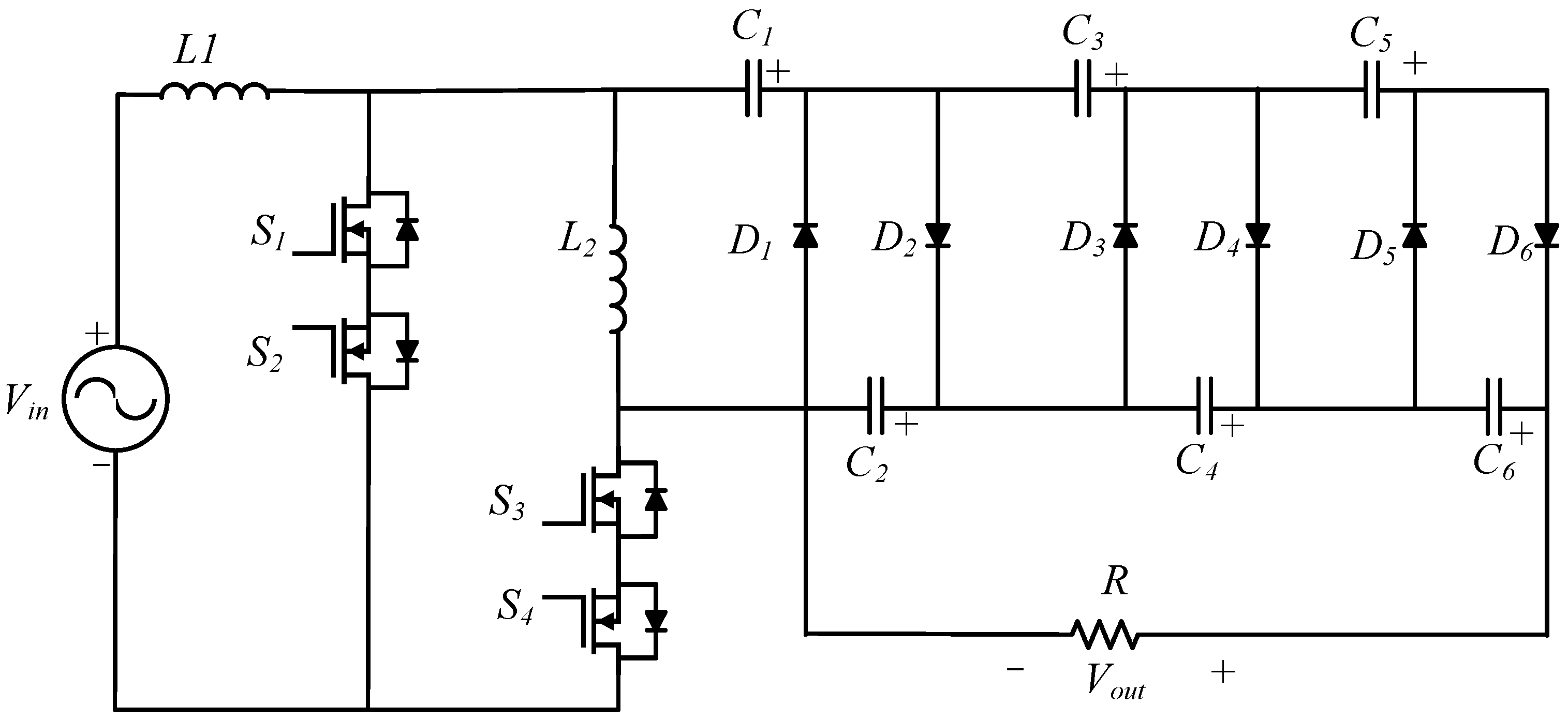
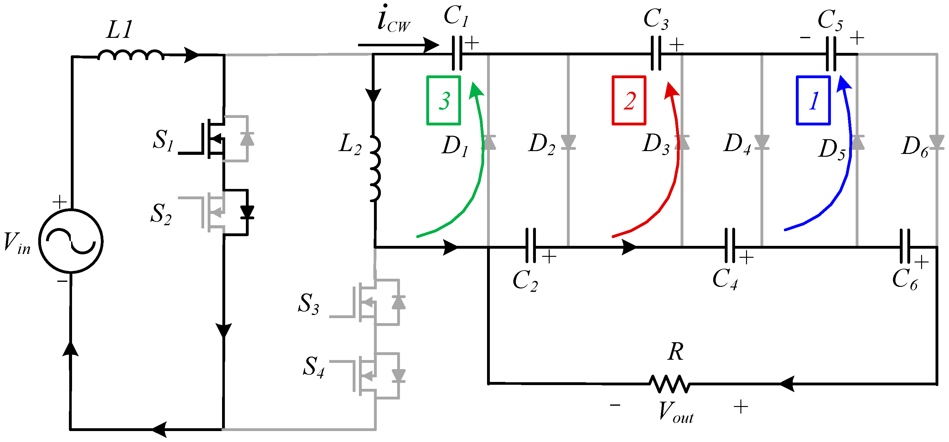
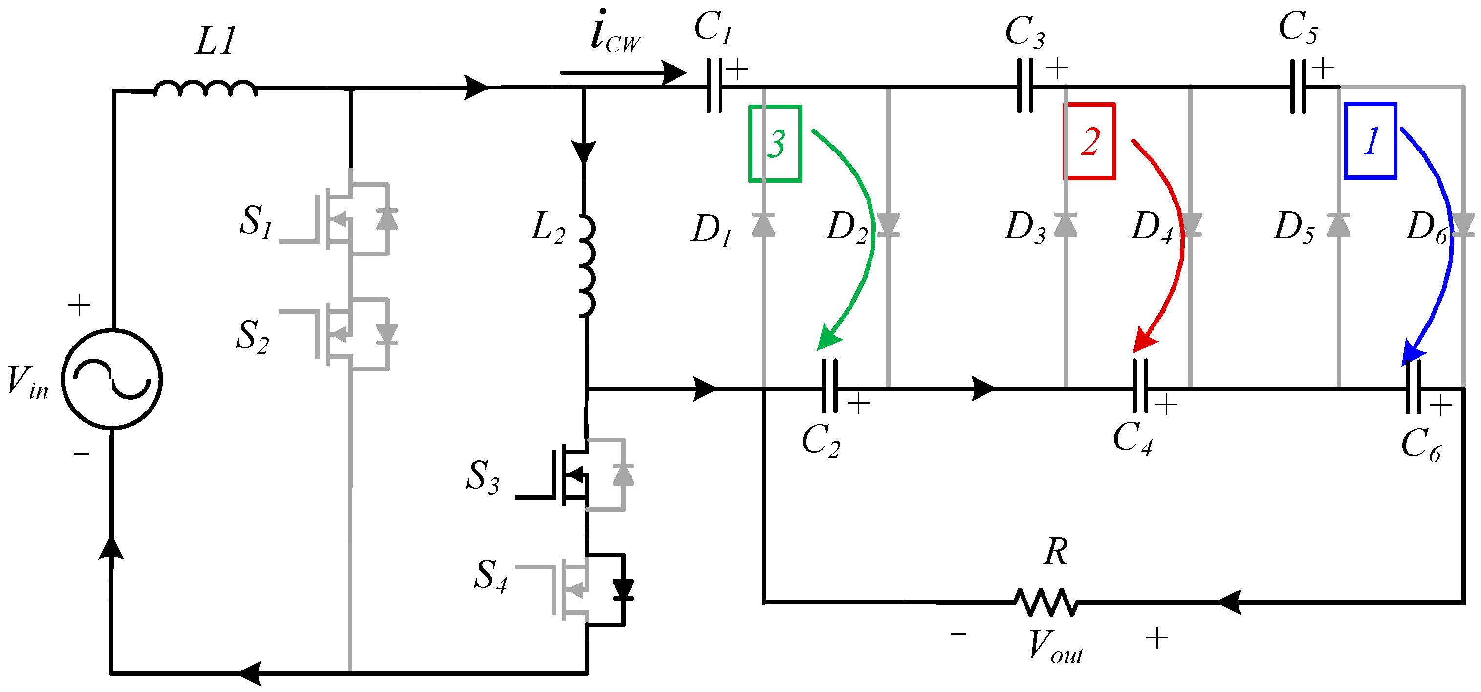
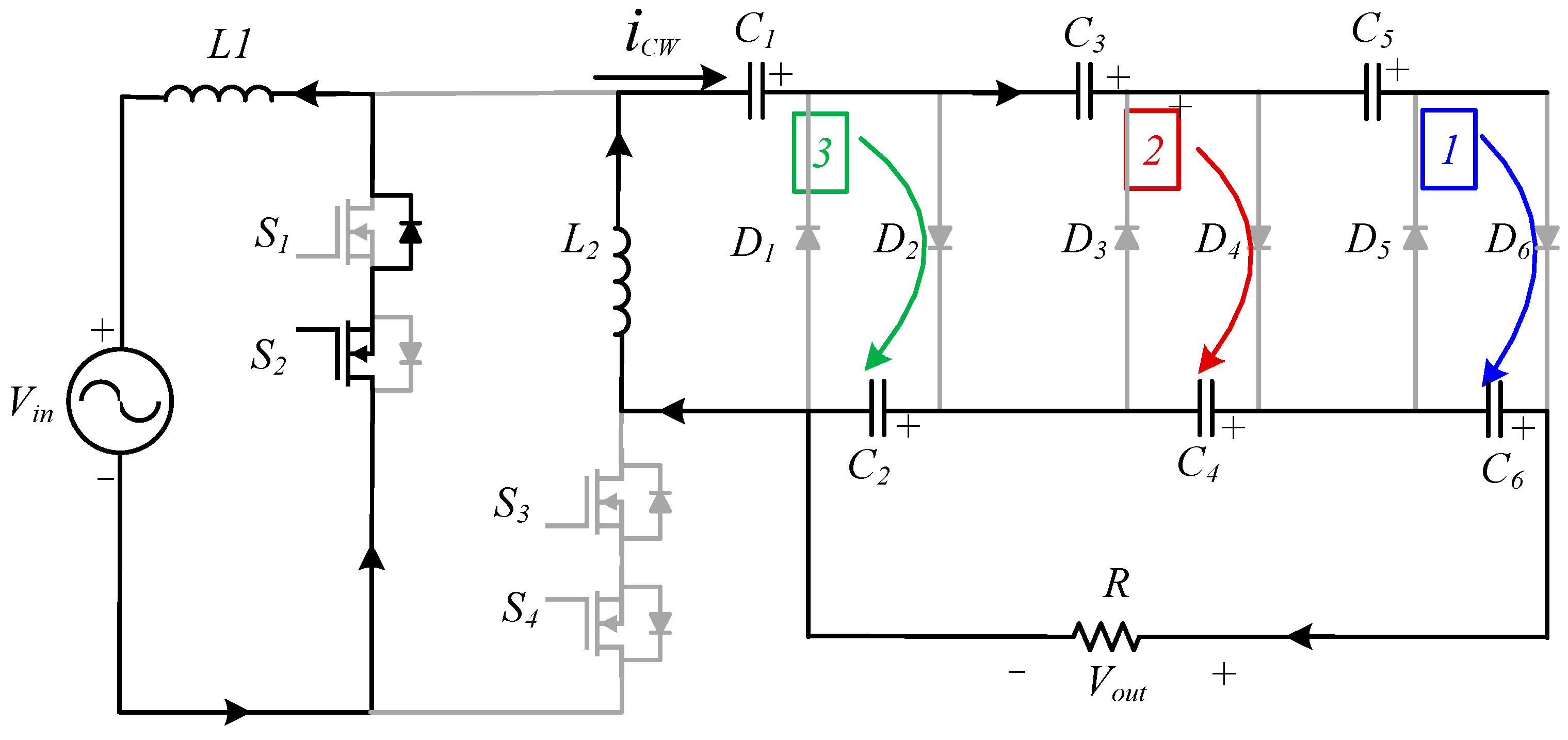
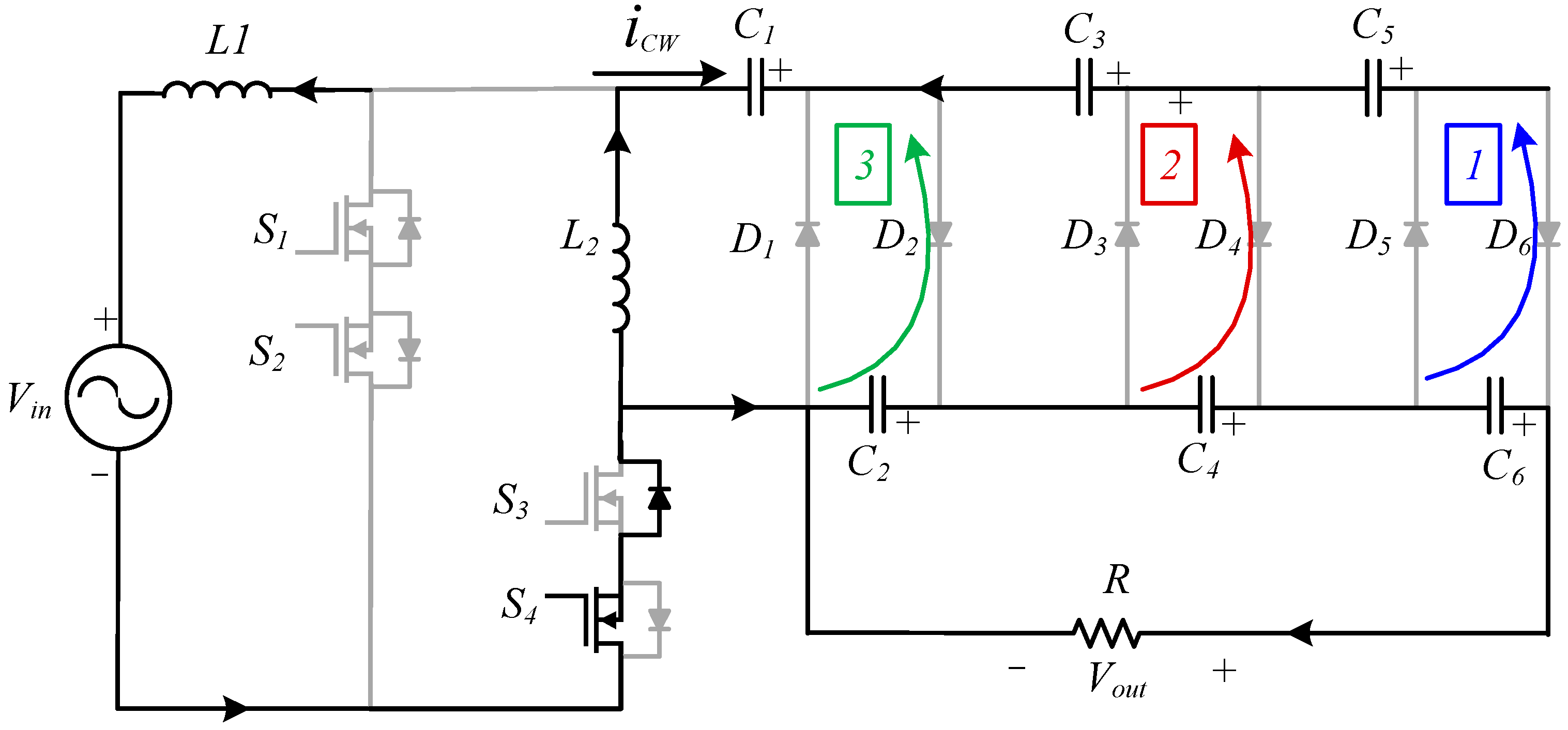
2. Steady-State Analysis

The suggested topology chiefly consists of a cascaded one-phase converter along with a conventional three-stage Cockcroft-Walton voltage multiplier, as seen in Figure 1. The single-phase converter is built with four bidirectional switches, separated into four denoted sets as S1, S2, S3, and S4. The proposed converter is invigorated to boost operation using the line-frequency AC source with a series inductor.
The following hypotheses are assumed for the study of the suggested converter’s steady-state behaviour:
  • The whole capacitors in the Cockcroft-Walton voltage multiplier are big, and every capacitor’s voltage drop and ripple could be ignored under a suitable load condition;
  • The whole circuit elements are ideal, and the system is without power loss;
  • The suggested converter operates in continuous conduction mode (CCM), and also in the condition of a steady-state;
  • Ignoring safe commutation states (overlap time);
  • All values of capacitors are equal.
According to [7,20,21], the voltage ratios of capacitors are equal to:
V C k = { V o / N f o r k = 1 N = 2 n 2 V o / N f o r k = 2 , 3 , , N .
In relation (1), N is the number of circuit layers that multiplies the CW voltage and Vo is the circuit’s output voltage. Also, VCk is the kth capacitor voltage. In the CW multiplier circuit, the output voltage is similar to the sum of the voltages of the series capacitor connected to the multiplier and is equal to:
V o = V C 2 + V C 4 + V C 6 + + V C k .
As voltages of all capacitors are the same except for the first capacitor, the output voltage of CW multiplier circuit is equal to:
V o = n V C k = N V C 1 = N V γ ,
where V γ is the input voltage of the CW circuit.
The performance of the CW multiplier circuit will be investigated in two modes: negative and positive half-cycle of input voltage. In the positive half-cycle, S2 and S4 switches are off and the S1 and S3 switches are in switching mode. The circuit in the positive half-cycle is analysed in two modes.
In the first state, when the S1 switch is on, the S2, S3, and S4 switches are off; also, L1 inductor current passes through the S1 and S2 switches, then the L1 inductor is charged, and its current increases. During this period, the L2 inductor supplies and discharges the CW multiplier current, in the CW current flow in Figure 2, respectively, and is at the positive half-cycle. In this case, the voltage across the inverter L1 is equal to:
V L 1 = v i n ,
where vin and VL1 are the input voltage and the voltage across L1 inductor, respectively, and the inductor voltage L2 is equal to:
V L 2 = V C 1 = V o N ,
and capacitor current C1 is in the opposite direction of IL2 current.
i C 1 = i L 2 .
The second state also occurs in the positive half-cycle, while S1 is turned off and the S3 switch is turned on; S2 and S4 switches are still off. In this case, the L1 inductor current is injected into the Cockcroft-Walton multiplier circuit as well as the L2 inductor. Therefore, the L1 inductor is discharged and the L2 inductor is charged, which is shown in Figure 3, respectively, in the positive half-cycle.
In this switching interval, VL1 is equal to:
V L 1 = v i n V C 2 + V C 1 = v i n V o N ,
and the voltage of the inductor L2 (VL2) is equal to:
V L 2 = V C 1 + V C 2 = V o N ,
also, the current of capacitor C1 (iC1) is achieved as follows:
i C 1 = i L 1 i L 2 .
the same analysis can be done for the negative half-cycle in two cases.
The third state occurs when the S2 switch is on, the S1, S3, and S4 switches are off, the current of inductor L1 passes through the S1 and S2 switches, and then the inductor L1 is charged in the negative half-cycle, increasing its current. During this period, the L2 inductor supplies and discharges the current of the CW multiplier, which is demonstrated in Figure 4, respectively, in the negative half-cycle.
The fourth state occurs in the negative half-cycle while the S2 switch is off and the S4 switch is on, and the S1 and S3 switches are still off. In this case, the L1 inductor’s current is injected into the Cockcroft-Walton multiplier circuit and is discharged. Then, the L2 inductor is charged, which is shown in Figure 5, respectively, in the positive half cycle.
The converter analysis is carried out for the negative and positive half cycles similar to each other. Applying the rules of the average capacitor’s current in a period, and using Equations (6) and (9), we have:
< V C 1 > = 0 ,
i L 2 D T S W + ( i L 1 i L 2 ) ( 1 D ) T S W = 0 ,
i L 2 = ( 1 D ) i L 1 .
The current ripple for L1 inductor’s current during 0 < t < D T s w is calculated as:
Δ i L 1 = v i n L 1 D T S W .
The TSW is defined as the switching period and the D is defined as the duty cycle.
The current ripple during this interval ((1 − D) TSW) is equal to:
Δ i L 1 = v i n V o N L 1 ( 1 D ) T s w .
Regarding the switching frequency, that of 1/TSW is very high (about 150 kHz), and it can be assumed that the amount of charge and discharge of L1 inductor is equal in the switching period as well as that the average current during a TSW period must be zero, and therefore, we have:
v i n ( t ) L 1 D T s w + v i n ( t ) V o N L 1 ( 1 D ) T s w = 0 ,
v i n ( t ) = V o N ( 1 D ) ,
V o v i n ( t ) = N 1 D ,
where Equation (17) shows the relationship between output and input voltage. Assuming that output power is equal to the input power of the CW circuit, then:
V o I o = V i n R M S I i n R M S ,
where VinRMS and IinRMS are the RMS values of input voltage and current, respectively. It should be noticed that the converter can be controlled in such a way that input current and voltage are in the same phase (converter conditions of power factor correction). Assuming resistance load, the value of output current is equal to:
i L 1 , max = 2 P o V i n R M S = 2 V o 2 V i n R M S R o ,
where Po, Ro, and Vo are defined as output power load resistance and output voltage, respectively. Also, the relationship between duty cycle D and instantaneous angle ( ω t ) is determined by Equation (20) and plotted in Figure 6.
D ( t ) = 1 V i n N V o sin ( ω   t 3 ) .
Regarding Figure 6, the value of the duty cycle in this converter is not constant and changes with time, and where the input voltage obtains its peak value, the duty cycle obtains its minimum value; also, while input voltage reaches the maximum value, the converter’s switching frequency increases and the duty cycle changes in each half-cycle, and it is symmetric with respect to tw = 90. Furthermore, the number of CW converter stages increases and the duty cycle changes in one-half cycle. This also shows the changes in the duty cycle of the boost converter, and the traditional boost converter in the duty cycle provides a higher duty than the output voltage converter provided. Figure 7 illustrates the voltage and current of switches the state of the converter in different scenarios.

3. Design Considerations

3.1. Components Determination

In general, it is vital to specify the minimum values of capacitors and inductors based on current and voltage ripples, as well as current and voltage stresses of semiconductors to construct a power electronic converter. In this section, the parameters listed in Table 1 will be used to design the converter.
First, we try to calculate the L1 inductor’s value. The maximum input current value of the circuit is equal to:
i L , max = 2 P o η v i n , r m s = 2 × 1000 0.9 × 220 = 7.142 A ,
where ɳ is the converter efficiency. The relationship between voltage and current of the inductor can be described as follows:
V L 1 = L 1 Δ i L 1 Δ t ,
L 1 = V L 1 Δ t Δ i L 1 ,
L 1 = v i n ( t ) D ( t ) T S W K i I L , max = V i n , R M S 2 sin ( w t ) × [ 1 ( V m 2 N V o sin ( w t ) ) ] T S W K i I L , max .
The Ki value is the peak–peak change coefficient of the inductor’s current, which is 0.05 times the input current, and then:
d L 1 d t = ( v i n ( t ) D ( t ) T S W K i I L , max )         = ( V i n , R M S 2 sin ( ω t ) × [ 1 ( V i n , R M S 2 N V o sin ( ω t ) ) ] T S W K i I L , max ) = 0 , sin ( ω t ) = 1 2 V i n , R M S 2 N V o ω t = sin 1 ( 1 2 V i n , R M S 2 N V o ) = 74.63 o .
According to the relations (21) and (22), the value of L1 = 2.8 mH is achieved.
Then, for calculating the L2 inductor value, we have:
i L 2 = ( 1 D ) i L 1 ( 10 ) i L 2 = ( V i n N V o sin ( ω t ) ) ( I L 1 , max sin ( ω t ) ) i L 2 = V i n N I L 1 , max V o sin 2 ( ω t ) .
The maximum value of IL2 occurs at ωt = 90 with respect to the relation (26); therefore, the maximum value of IL2 is equal to:
i L 2 , max = V i n N I L 1 , max V o = 2.61 A .
Therefore, the value of L2 is equal to:
L 2 = V L 2 Δ t Δ i L 2 ,
L 2 = V o N D max T s w 0.1 i L 2 , max = 9.7 m H .
The capacitor value in the Cockcroft-Walton converter is achieved by the ripple of the suitable output voltage. The voltage ripple and drop related to each capacitor could be achieved under the steady-state using the charging–discharge behaviours of capacitors. The KRF is output voltage ripple coefficient, and if it is considered as Δ V 0 V o < 0.1 , then the value of capacitor C2 is calculated as follows:
C 2 > | T s w I o 2 V o K R F [ 4 N I o ω ( T s w 4 4 N V m 3 s V o ) 1 ] | C 2 > 374.3   μ F .
In addition, it is clear that if the capacitor value in the multiplier circuit is higher, then the output ripple of the circuit is lower; therefore, the 470 µF capacitors are used for the converter and other capacitors are chosen with the same value.

3.2. Voltage and Current Stress of Components

-
S1, S2, S3, S4 switch
The highest current passing through these switches is equal to the highest input current. According to (21), the maximum current passing through these switches is 7.142 A, and regarding the operation of the circuit when these switches are off, the input voltage of the CW multiplier circuit falls on these switches. The amount of voltage stress on these switches depends on the number of stages of the CW circuit. For a converter with one stage, the highest voltage stress on these switches is equal to 600 V.
-
Diodes
All the diodes in the steady-state operation convey similar charge over the period, i.e., similar average current. Consequently, since IL1 is equal to the average half-wave input current of the CW converter, the average current flowing in all diodes can be calculated during period T [38]:
I D = i L n .
-
Capacitors
In an n-stage Cockcroft-Walton circuit, given that the capacitors are large enough, all capacitors ideally maintain similar voltage except the first one, which has half the others. Consequently, the voltage stress on each capacitor is Vo/n, except for C1, where the voltage stress is achieved as (1 − D) Vo/n.
Voltage stress on capacitor C2 is achieved as 1260 V, and the voltage stress on capacitor C1 will be equal to 660 V for KRF = 0.1 based on (1).
-
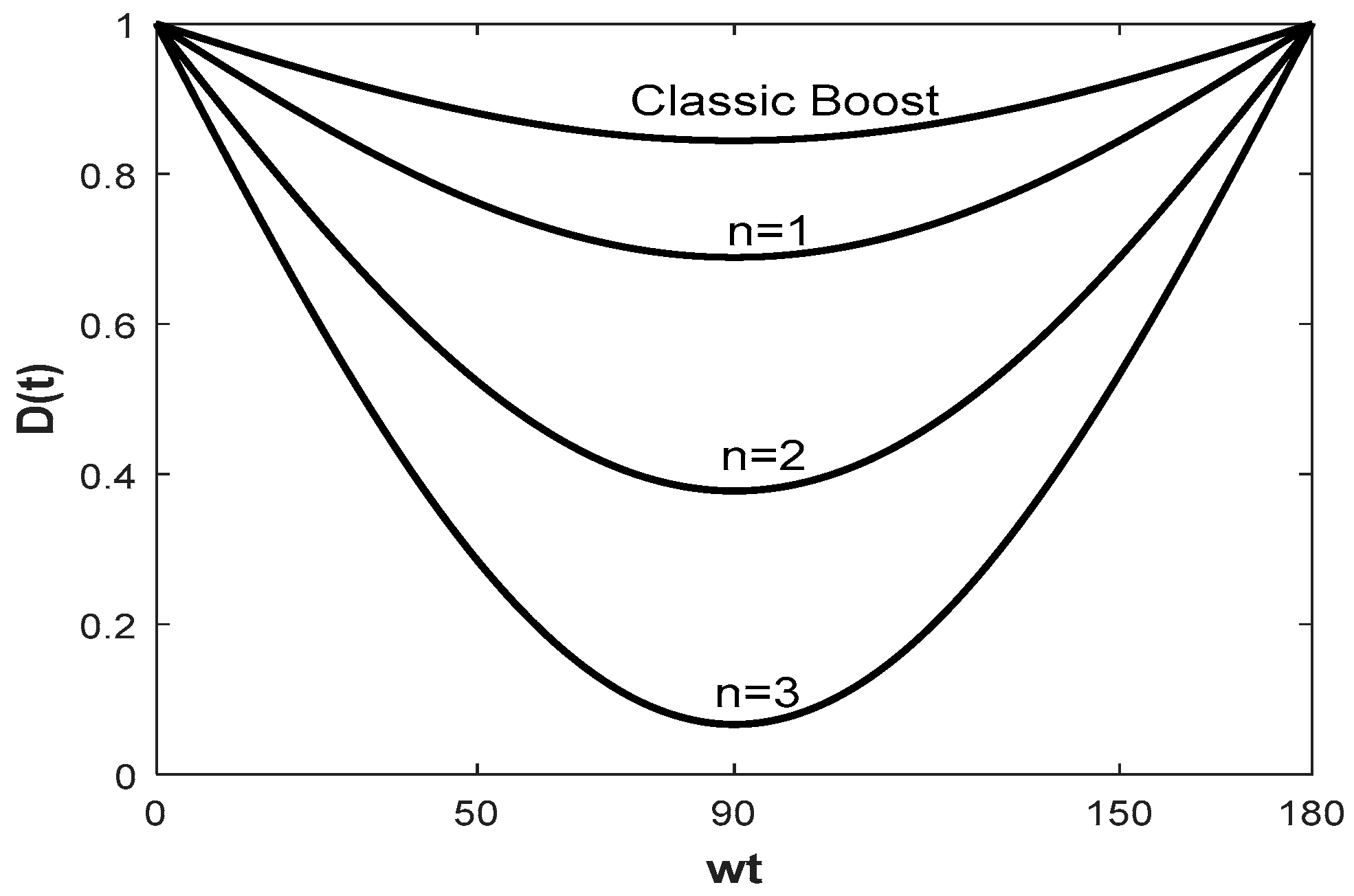
The number of n-stage
It is necessary to consider, in using Cockcroft-Walton, that the number of diodes enlarges to grow the DC gain by increasing n, and, thus, conduction loss of diodes will increase. This could lead to a reduction in overall performance. However, it is necessary to know that a lower number of n would result in higher voltage stress on the MOSFETs (need MOSFET with higher voltage rating) and, also, would result in increased power loss (conduction and switching) of MOSFETs. Hence, the trade-off between power loss of MOSFET and diodes must be performed in order to retrieve a suitable number of n. In practice, the converter is not ideal and has parasitic elements that cause the converter to have losses and decreases the converter voltage compared to the ideal condition.

3.3. Effect of Non-Idealities Components

The results of parasite elements on the suggested converter are investigated to achieve suitable comparability and practical insight. The parasitic elements that are discussed can be defined as: on-state resistance of switches Ron, forward voltage of the diodes VD, and winding resistance RL1 and RL2. According to these elements, the converter main losses are as follows:
  • • Losses due to switches;
  • • Losses due to inductor resistance;
  • • Losses due to diodes.
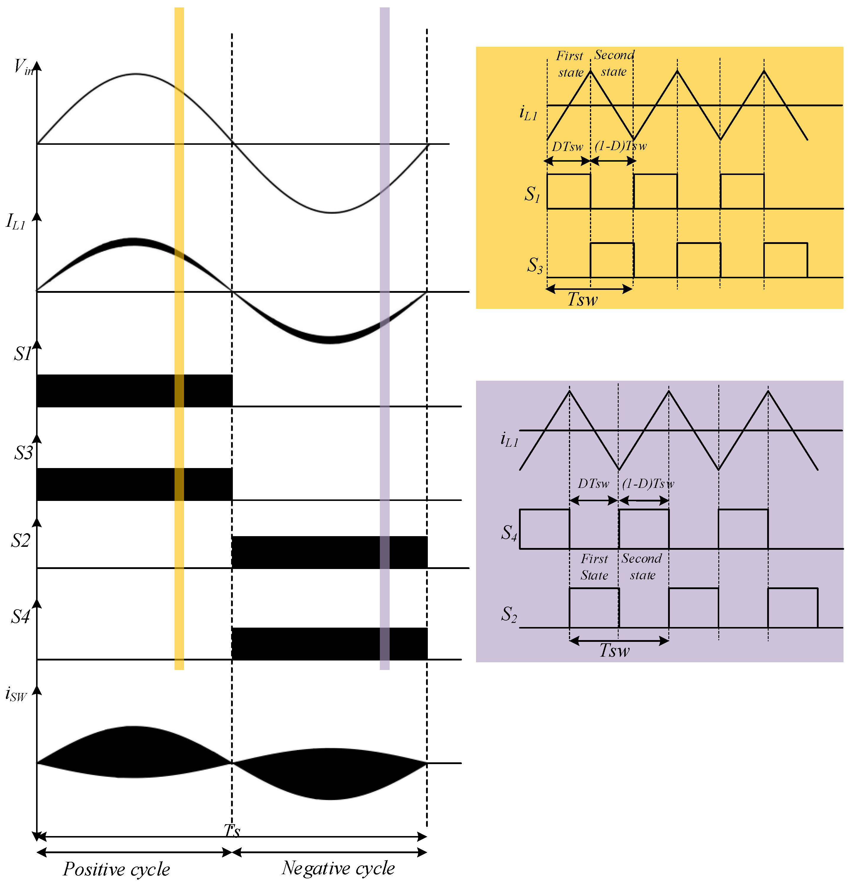
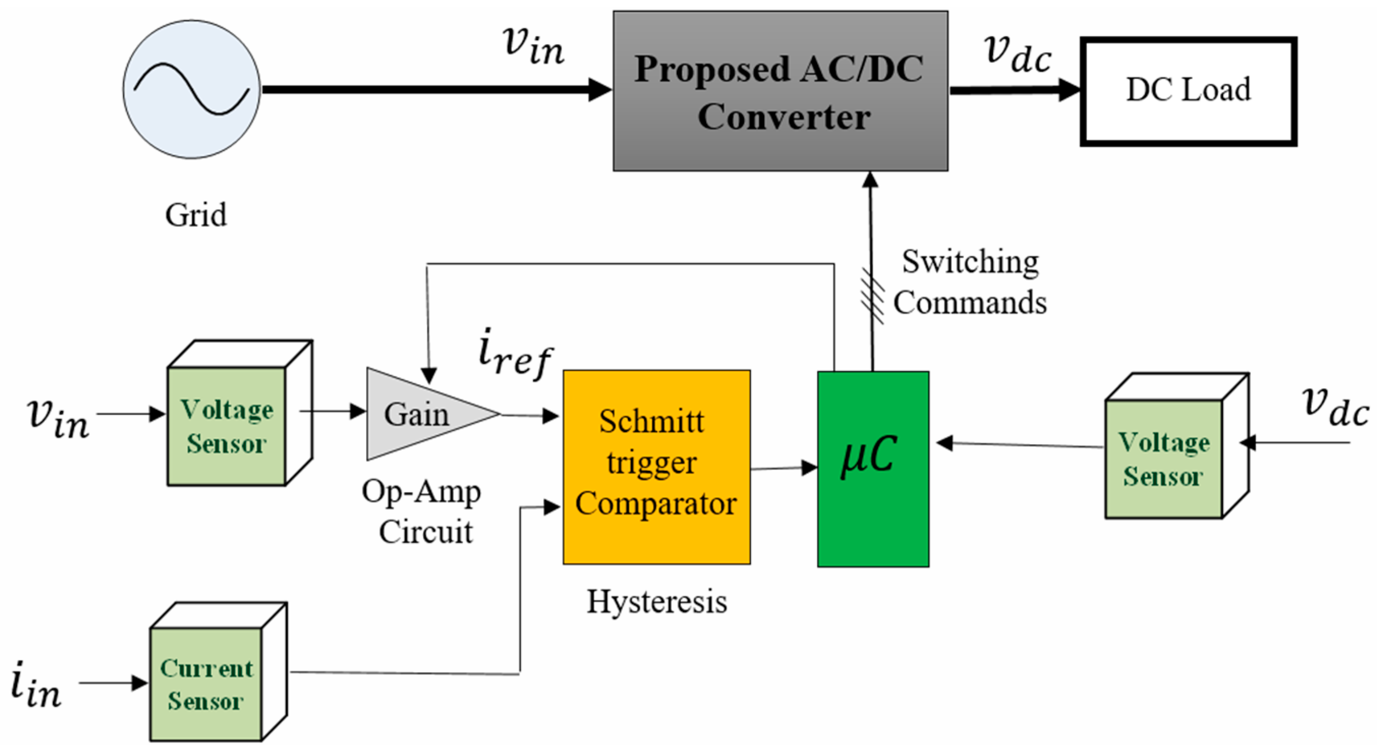
Power switch losses are divided into two types of switching losses and conduction losses. The conduction losses for the switches are equal to:
P l o s s , f = R o n I s w , R M S 2 = P c o n d ( s 1 , s 2 ) = R o n ( i L 1 , max 1 2 + 3 N 2 V 2 i n 8 V o 2 ) 2 , P c o n d ( s 3 , s 4 ) = R o n i 2 L 1 , max ( N V i n 6 4 V o ) 2 .
and the switching loss is equal to:
P l o s s , s w = 1 2 f s w V S W I S W [ t o n + t o f f ] ,
t o n = t r i + t f v ,
t o f f = t r v + t f i ,  
tri is the time interval of the switch transition from zero voltage to the nominal value and tfv is the time interval of the switch transition from the nominal value to zero. tfi is equal to the time duration that it takes for the switch to flow from the nominal value to zero and trv is for the time duration that it takes for the switch voltage to go from zero to the nominal value.
The loss of the inductors depends on their resistance as well as the current that passes through them:
P c o n d , L 1 = R L 1 I 2 L 1 , R M S = R L 1 I 2 i n , R M S , P c o n d , L 2 = R L 2 [ V i n N 6 4 V o i L 1 , max ] 2 .
Moreover, diodes have two types of loss. Diode conduction losses and loss of diode relate to the on and off.
The conductive losses of the diodes in the half-cycle are equal to:
P l o s s , D = 2 T s [ 0 T s / 2 D ( t ) i L 2 ( t ) V D d t + 0 T s / 2 ( 1 D ( t ) ) ( i L 1 ( t ) i L 2 ( t ) ) V D d t ]             = 2 T s 0 T s / 2 ( 2 D ( t ) ) i L 2 ( t ) V D d t = N V i n V D V o i L 1 , max [ T s 2 4 V i n N 3 ω ] ,
and the losses due to switching on and off the diodes are equal to:
p r r = 2 n f s Q r r V o n = 2 f s Q r r V o ,
where Qrr is the recovery charge of each diode that is determined by the diode datasheet.

4. Control Strategy

In the proposed converter, the hysteresis method is used for controlling the circuit. Hysteresis current control is a suitable switching method used in all types of structures for managing the current of power converters due to its simplicity, high stability, fast dynamic behaviour, and high accuracy. According to the performance of the circuit, when the S1 switch is on in positive half-cycle (S2 switch is on at negative half cycle) and the S3 switch is off (S4 switch is off) in Figure 3, the L1 inductor is charged and its current increases, and when the S3 switch on the positive half-cycle is on (S4 switch on the negative half cycle is on) and the S1 switch is off (S2 switch is off) in Figure 4, the L1 inductor is discharged and its current decreases. The principle of the hysteresis method in this converter is that a single-phase sinusoidal reference wave is compared with the input voltage (reference current) with the inverted L1 current. A hysteresis bandwidth is considered to be limited between the upper and lower band. The performance of the converter in negative and positive half-cycles is as follows.
First mode in the positive half-cycle: reference current is evaluated with inductor current L1. If the L1 inductor current reaches the upper hysteresis band, the S3 switch turns on and the S1 switch turns off, and the L1 inductor current decreases, and if the input current L1 reaches the lower hysteresis band, the S1 switch turns on and the S3 switch turns on. It turns off and this process continues until it enters the negative half cycle.
The second mode in the negative half-cycle: this mode is similar to the previous mode and the reference current is compared with the input current of L1. If the L1 inductor current reaches the upper band, the S2 switch will turn on and the S4 switch will turn off. Also, if the input current reaches the lower band of the L1 current, the S3 switch will turn on and the S2 switch will turn off.
If the hysteresis bandwidth is high, the switching frequency will decrease and the THD of the current source will increase. If the hysteresis bandwidth is low, the switching frequency will increase and, as the switching speed increases, the accuracy of the reference current will increase, and the THD of the current source will decrease; however, the problems caused by the increase in the switching frequency will increase.
The disadvantage of the hysteresis method is that the switching frequency varies, which causes noise and increases the switching loss, and injects high-frequency current components into the current source.

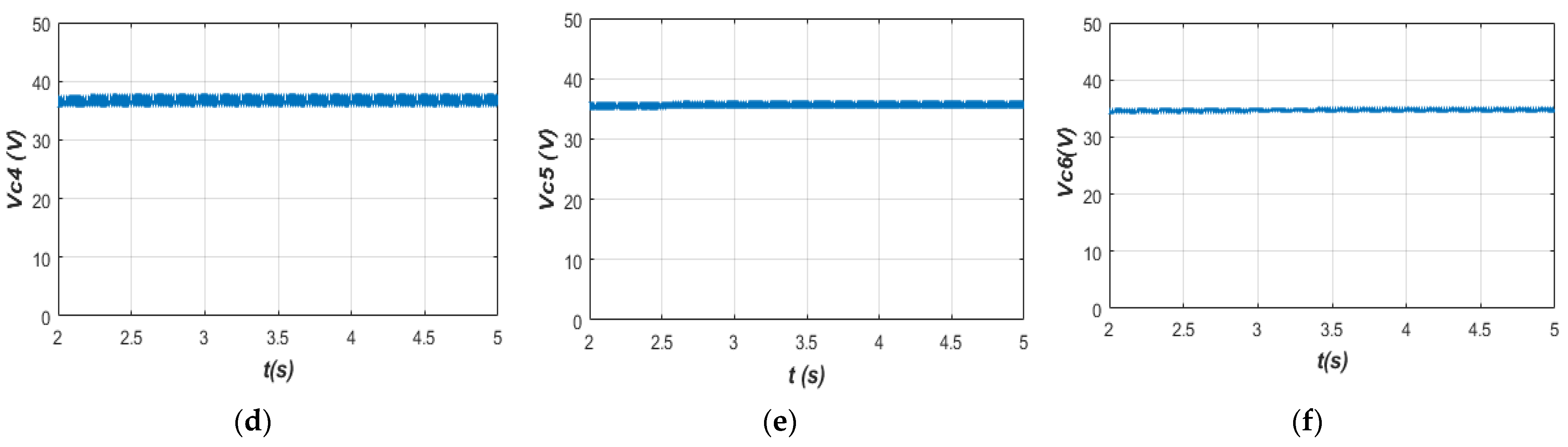
5. Converter Validation

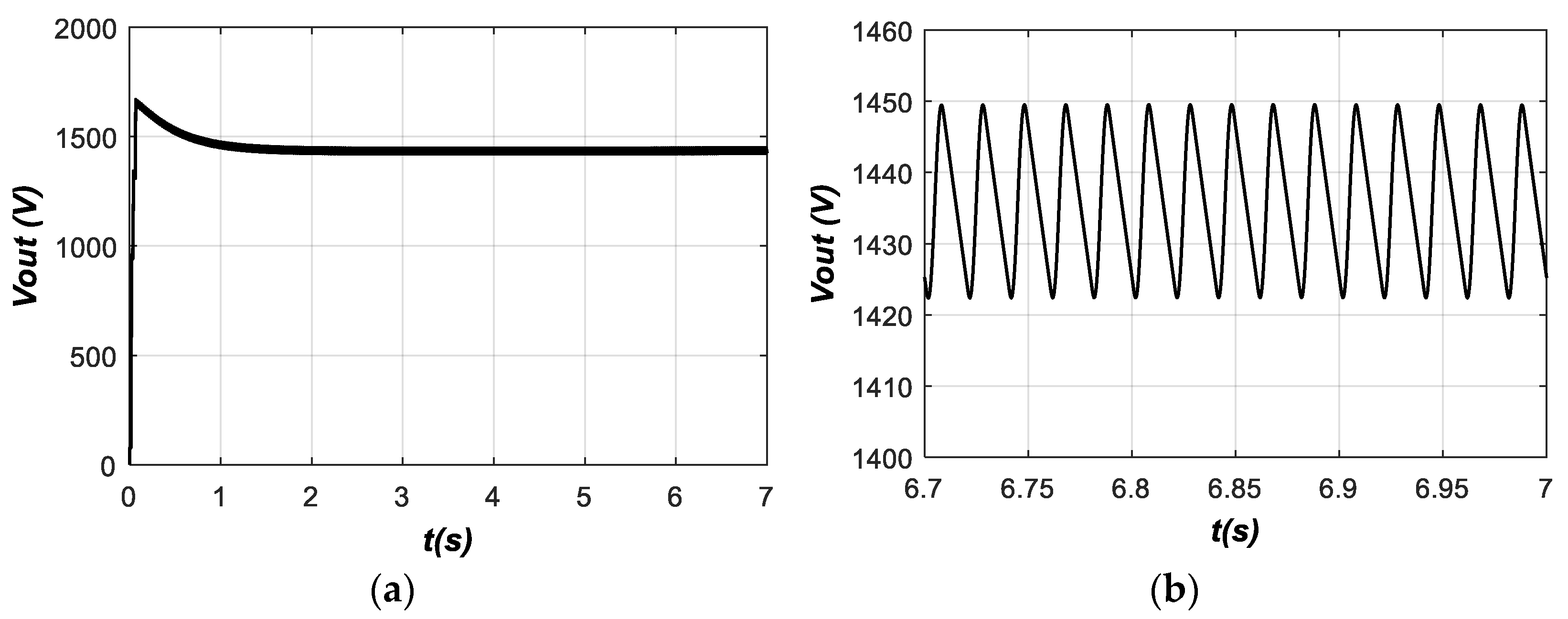
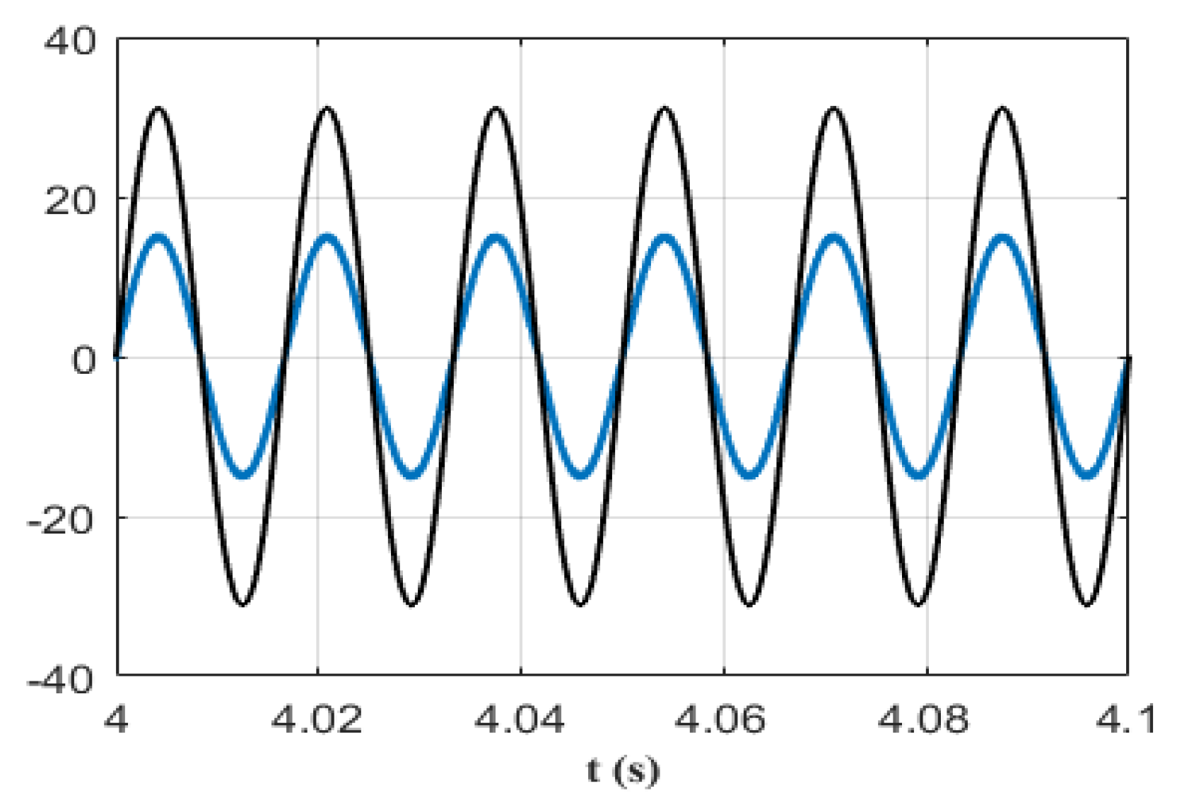
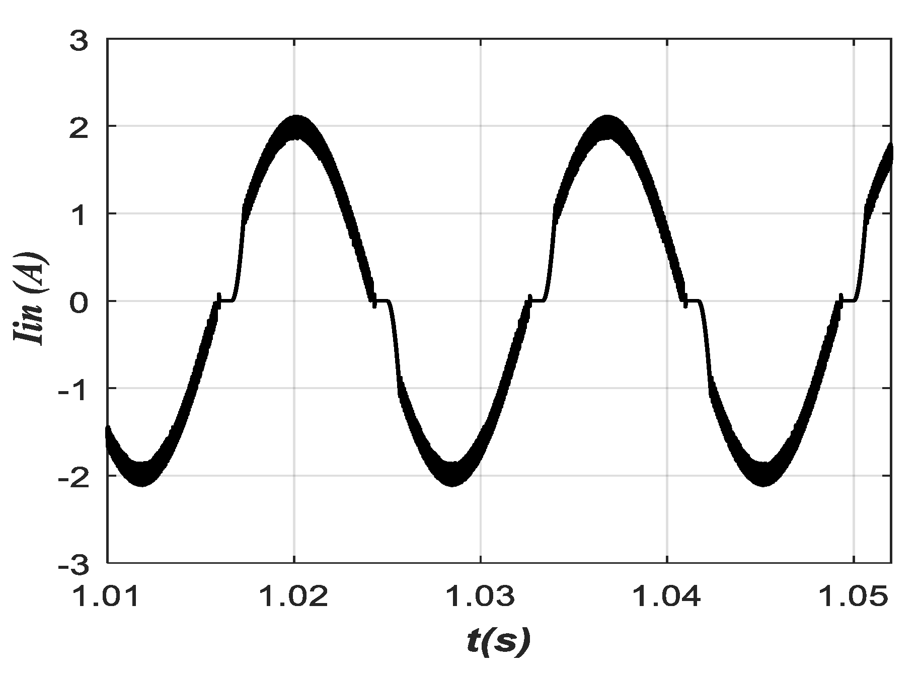
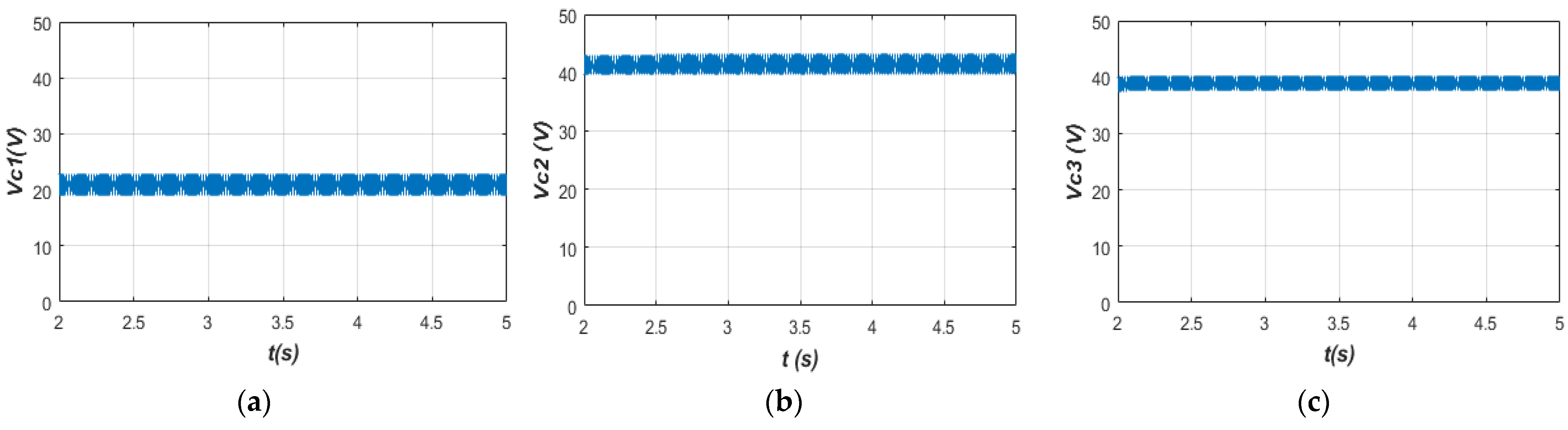
5.1. Simulation Results

A converter with a three-stage CW multiplier has been designed and simulated to assess the performance of the proposed converter. The size of the circuit elements is considered in Table 2 according to the values obtained from the theoretical results.
The simulation results of the converter are provided with the CW multiplier of one level; the value of the reference current is given to the converter with the desired line frequency and amplitude. Converter switching is aimed at tracking the input current of the converter. In this simulation, the multiplier of one level and the values of the convertor elements are simulated according to the values calculated in the previous section.
Figure 8 represents the implemented control scheme for the proposed converter in simulation and experimental results. We sample the input voltage and use it to determine the phase of reference current as of the input voltage and the input current should be in phase for PFC operation. The microcontroller determines the magnitude of the reference current waveform according to the required output voltage. The switching commands for S1 to S4 are generated by the microcontroller. Since the switching commands are generated by a current hysteresis algorithm, the switching frequency is not constant. Selecting a narrow hysteresis bandwidth reduces the THD value but increases the switching losses. Therefore, there is a tradeoff between output power quality and converter efficiency. The instantaneous value of the reference current is obtained by sampling the input voltage (to provide a power factor correction operating condition). In order to change the input current value, the reference current must be changed through the microcontroller. The hysteresis band for the experimental setup is adjusted to 0.2 Volts. The switching frequency is not constant but has an average value of 150 kHz. Figure 9 compares input current THD for two different current controls: (1) close-loop simple current control and (2) hysteresis current control. The input current THD was calculated to be 4.93% and 1.22% for the closed-loop control and hysteresis current control, respectively.
Figure 10a shows the amount of reference current with an amplitude of 15 A and Figure 10b shows the converter input current that the reference current follows, and as can be seen, the input current is sinusoidal. In Figure 11, the waveform of the converter output voltage is shown, and the output voltage of the converter is shown in Figure 9b. In Figure 12, the shape of the input voltage and input currents is shown simultaneously. As can be seen, the input voltage and input current are all-phase. The current of the L2 inductor is shown in Figure 13. As can be seen, due to the use of the hysteresis control method, the L2 inductor current is almost sinusoidal. The THD of the input current in this method is 1.22%, as shown in Figure 14.
In Figure 15a, the amplitude of the reference current changes from 10 A to 15 A after 5 s. As can be seen from Figure 15b, the value of the converter input current has also changed from 10 A to 15 A after 5 s.
The output voltage waveform is shown in Figure 16a, and the output current waveform is shown in Figure 16b; as expected, the value of current and voltage changes after 5 s and converge to new values.
Figure 10 and Figure 12 demonstrate that the converter is able to provide power factor correction in the AC side and track the reference current waveform with a neglected error. THD is also accepted as shown by Figure 14. For the output voltage, the ripple has good consistency with theoretical predictions (Figure 11).

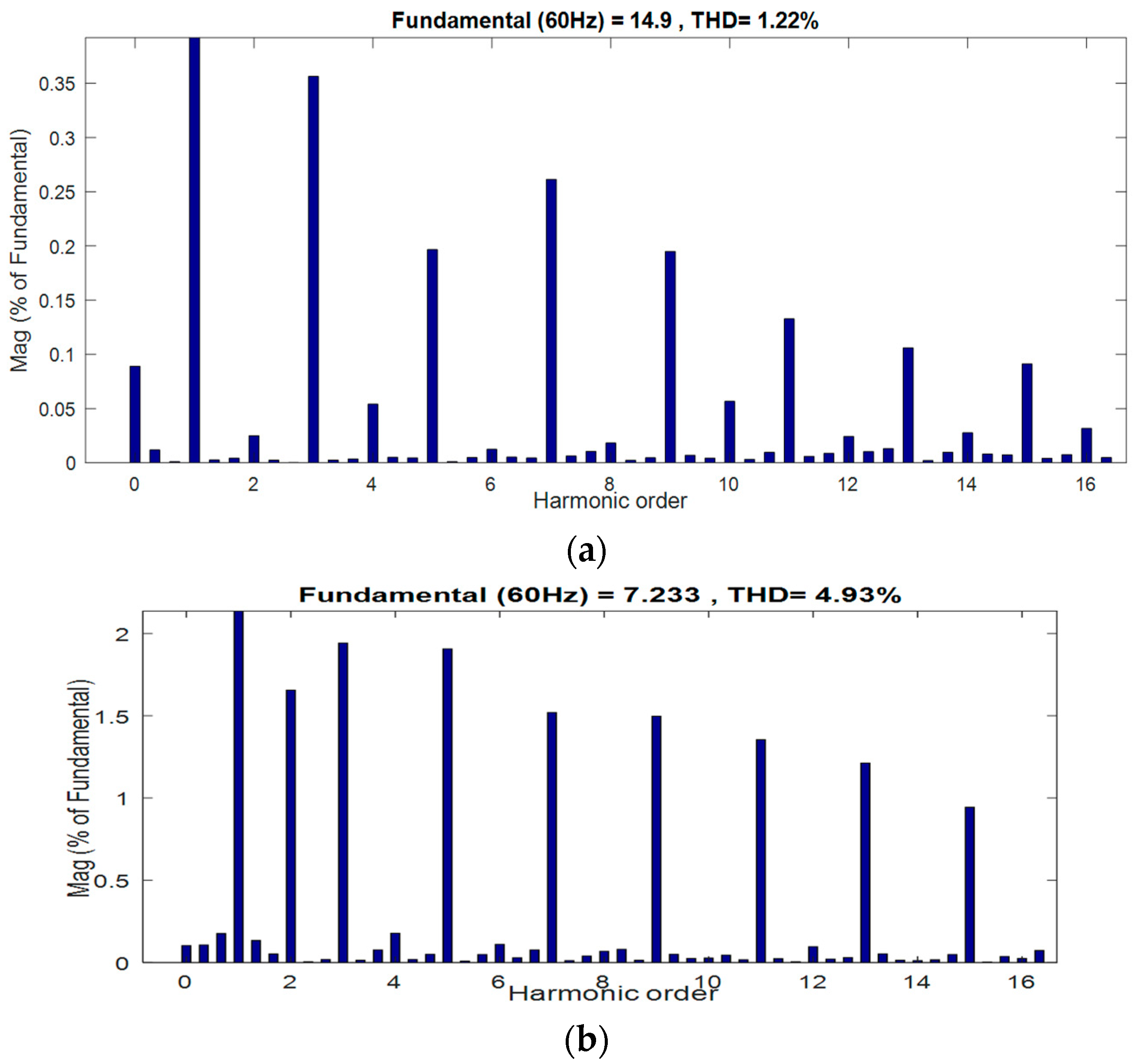
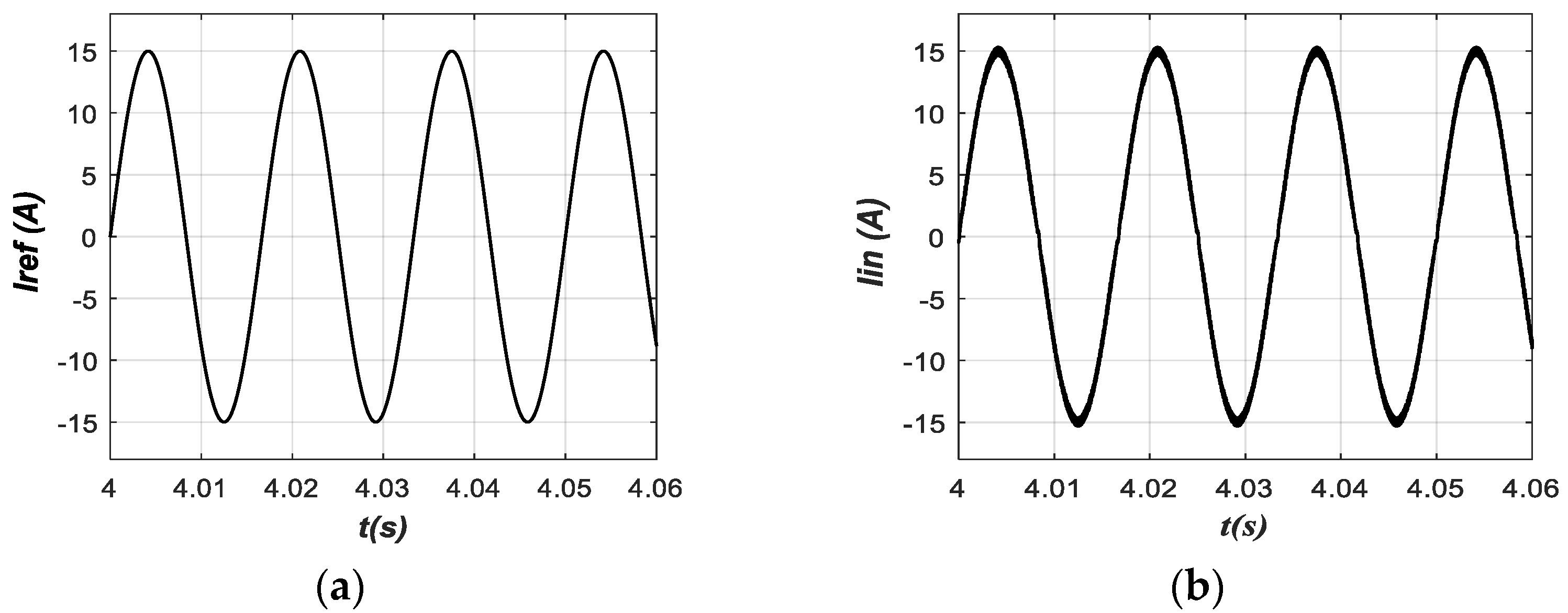
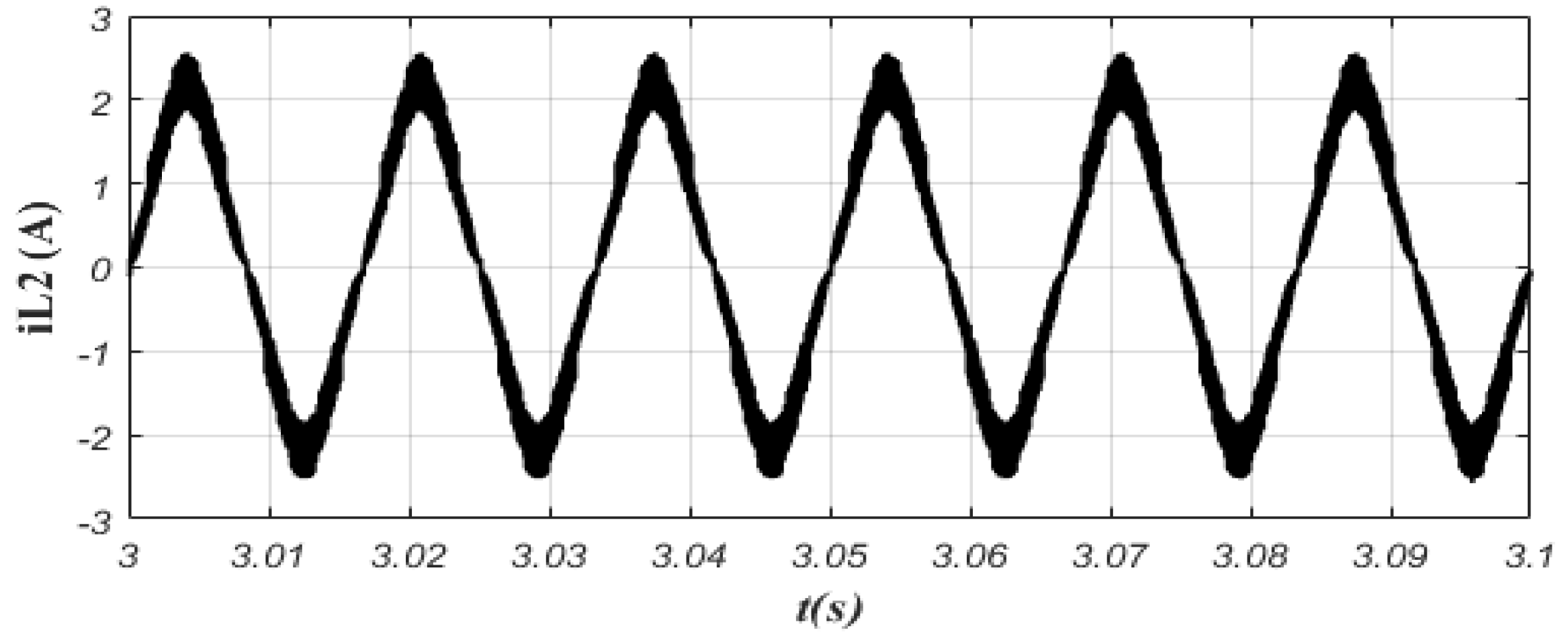
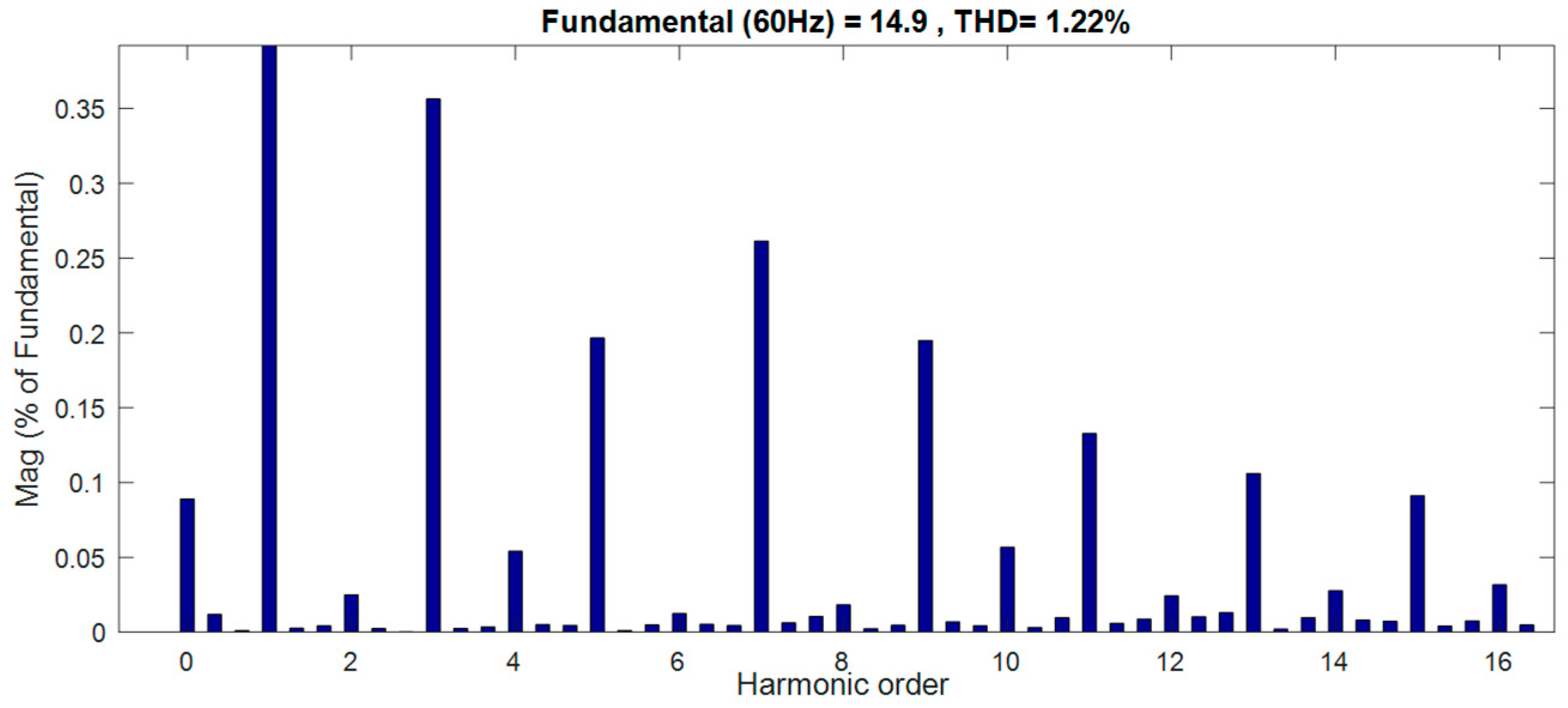
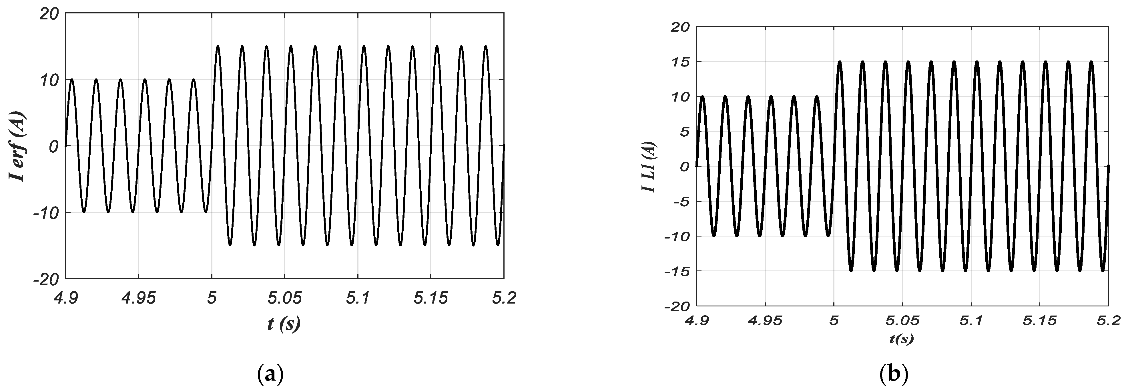
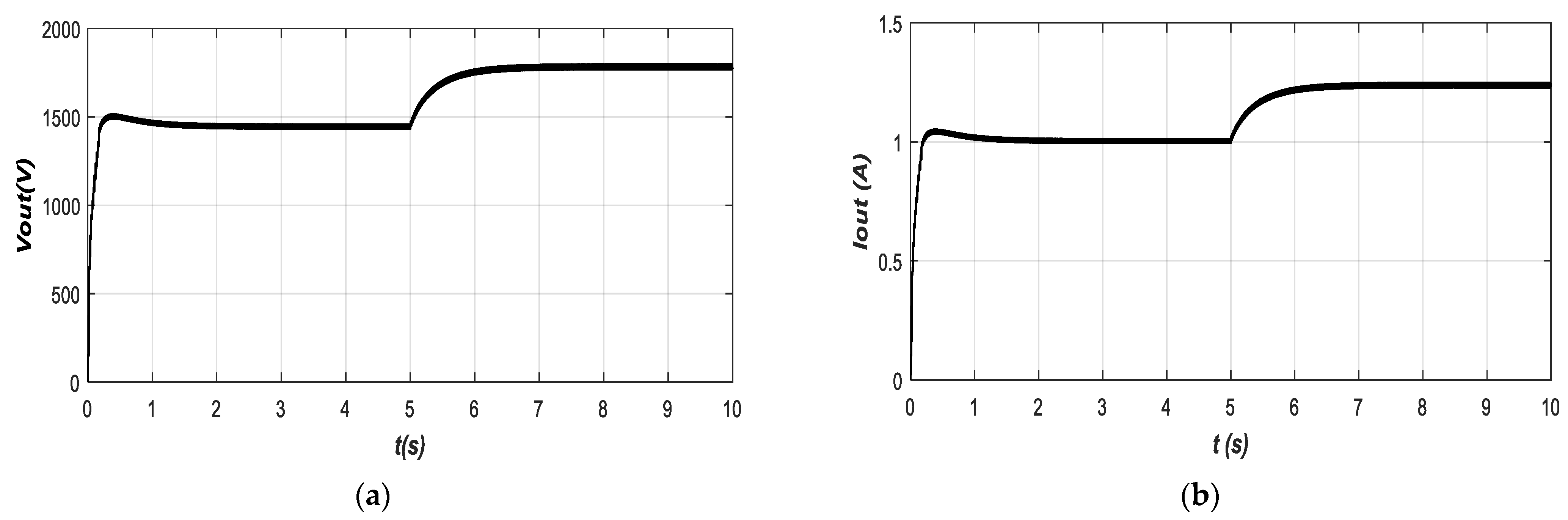
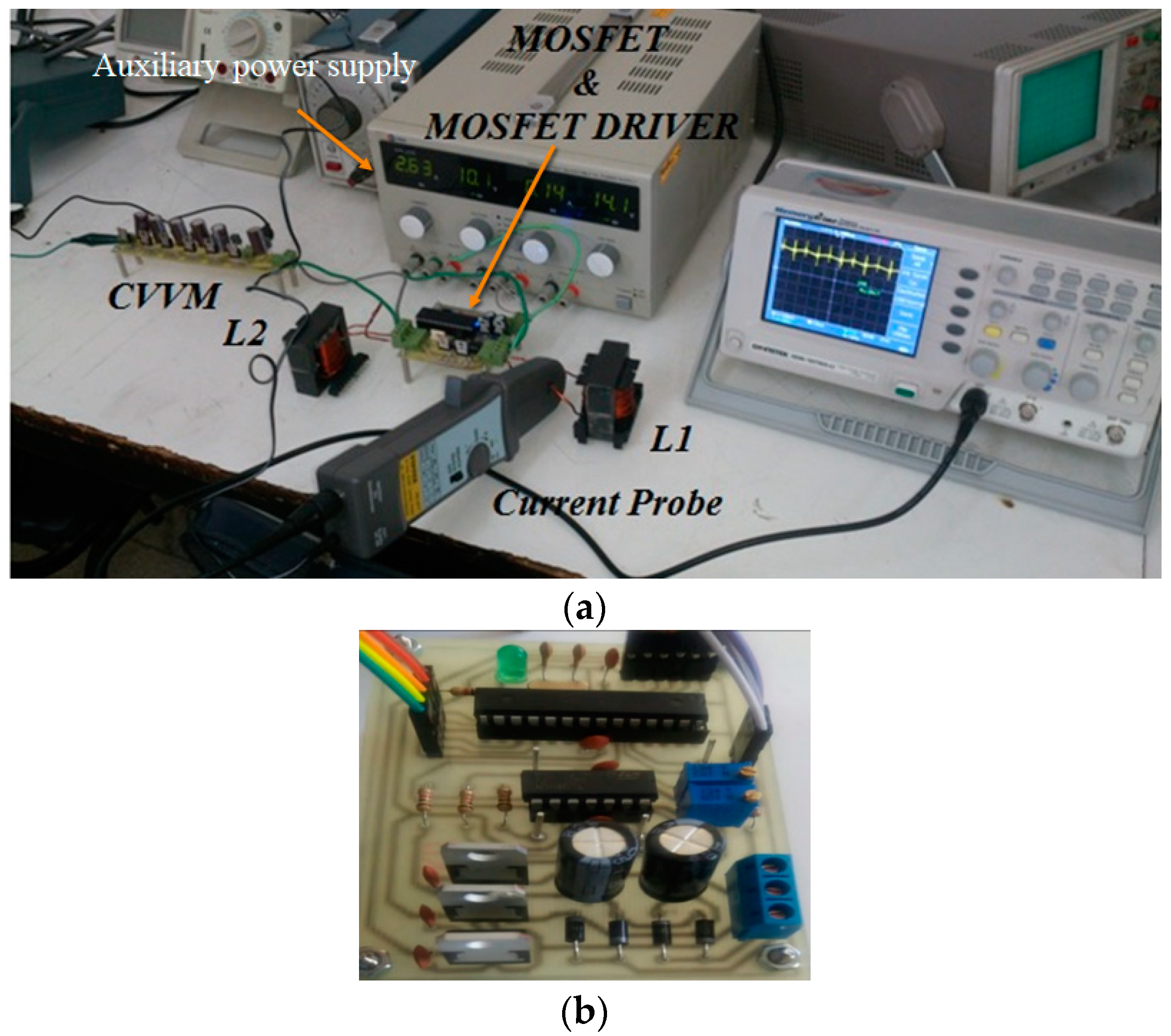
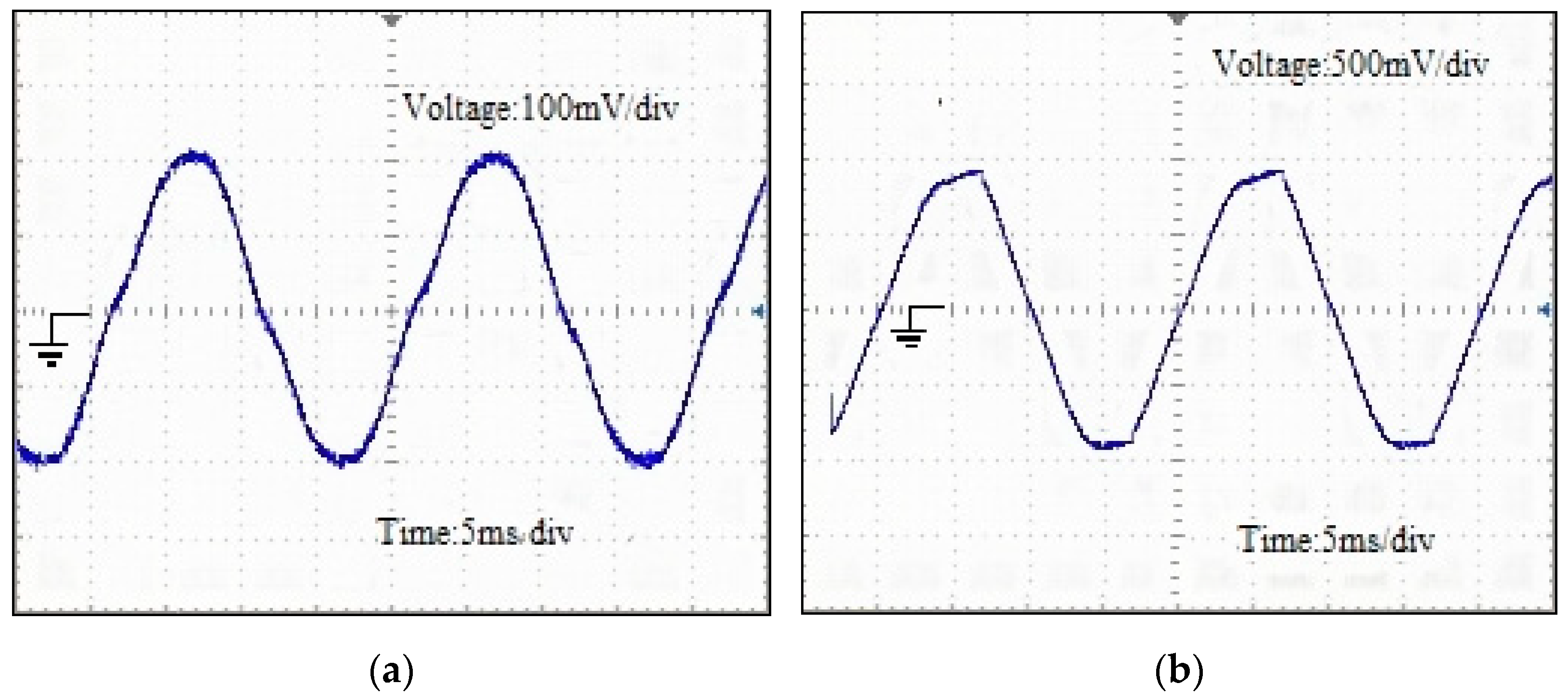
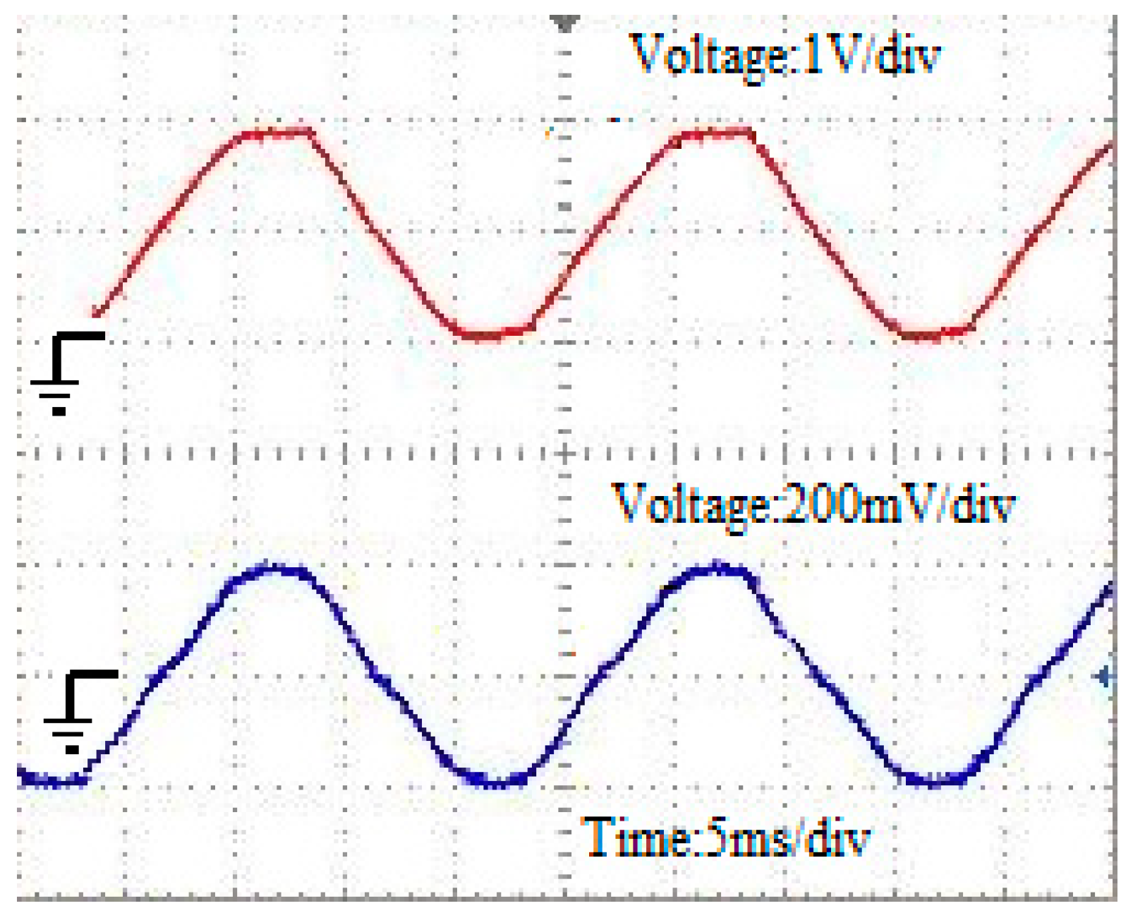
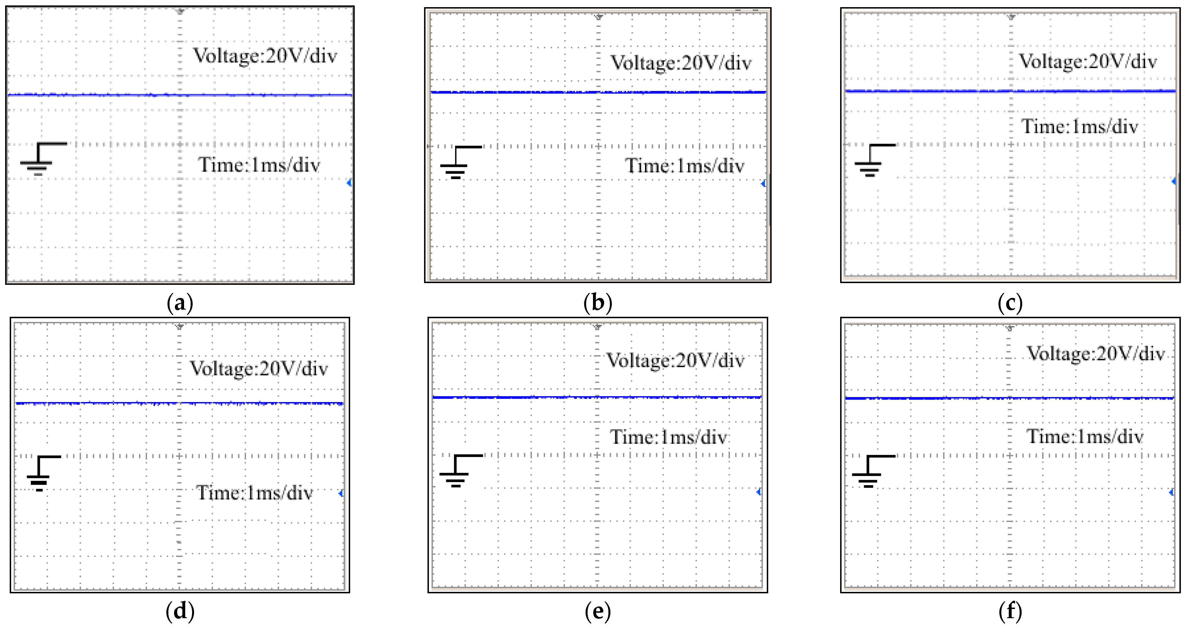
5.2. Experimental Results

A converter with specifications listed in Table 3 is provided for experimental validation of the theoretical part. This converter uses the hysteresis controller and the three-level multiplier. The prototype is shown in Figure 17.
The built-in converter has three parts. The first part is related to the CW voltage multiplier circuit and converter and load inductors, and the second part is related to the converter control section. The input voltage is applied to the microcontroller using a step-down transformer 220/9 V, resistive division, and op-amp circuits to the appropriate voltage level in order to generate the reference current and then the reference is entered into the microcontroller. The third part is related to converter switches with gate drives, which have separate sources due to the isolation of voltages related to gate drives. A heat sink has been used to increase the temperature of the switches.
The waveform of the reference current is shown in Figure 18a. The microcontroller determined the required current magnitude according to the feedback from the output voltage. As shown, in order to provide a 115 V in the output, it is required to inject a peak value of 4 A into the converter. This waveform is compared to the input current through the current sensor, and the appropriate switching commands are generated for the switches. The input current of the converter is shown in Figure 18b.
The reference current has the same phase as the input voltage because it is obtained by using a resistive division and only 2 V and above are given turns. The waveform of the input current and the reference current is shown in Figure 19. As can be seen, both are homogeneous. The upper waveform of Figure 19 is related to the reference current, and the lower waveform is related to the input current measured by the flow sensor.
Considering all the practical limitations, the input current of the converter is shown in Figure 19 (experimental result) and Figure 20 (simulation result). The voltage waveforms of the capacitors of the voltage multiplier circuit are shown in Figure 21. The capacitor voltage C1 is half the voltage of the other capacitors, as expected. The voltages of capacitors C2, C4, and C6 are reduced compared to capacitors C3 and C5 due to the fact that they provide output current which is shown in Figure 22.
The waveform of the transient and steady-state of the output voltage is shown in Figure 23a and the simulation state is shown in Figure 23b.
The input voltage of the converter is shown in Figure 24, which can be seen as the effective value of which is 5 V.
Finally, in order to obtain a better assessment for the power loss of the converter, converter power loss versus the output power, and also efficiency diagram based on the variation of output power, the overall losses based on the variation in output power are compared in Figure 25.

5.3. Comparison between the Proposed Converter and State-of-the-Art Rectifiers

Comparison between the proposed converter and state-of-the-art rectifiers in terms of voltage gain, voltage stress of components, and number of switches are presented in Table 4. The proposed converter voltage gain is higher than [45]. Also, ref. [46] shows a marginally higher voltage gain but the number of elements is higher, particularly in a higher number of stages. The number of elements for the proposed converter is lower than [47] while the other characteristics are the same.

6. Conclusions

In this paper, a new topology of AC/DC converter using a high-voltage CW multiplier structure is presented. The main benefit of the converter is providing high voltage gain and the ability to work in PFC conditions. Moreover, the CCM circuit operation, design considerations, operating range, and loss calculations were investigated. Experimental results are consistent with the theoretical analyses carried out throughout this paper. Also, a comparison between this converter and several other converters was demonstrated in order to evaluate the proposed topology with other methods. This converter has relatively few elements as well as a high output voltage and low stresses compared to other works. The output voltage of the converter was adjusted to 115 V and the voltage ripple was lower than 2%. The input current THD were calculated as 4.93% and 1.22% for the closed-loop control and hysteresis current control, respectively. Due to the increasing DC loads on the power system, it can be concluded that this converter can be used on a large scale in the power grid as well as for sustainable renewable energy which employs AC generators such as wind energy systems. Therefore, improving the performance of the converter and reducing losses as well as its implementation and construction must be considered.

Author Contributions

Investigation, A.Z. and A.R.; methodology, A.Z., M.S. and A.R.; supervision, A.R.; software, A.Z. and A.R.; validation, A.Z. and A.R.; writing—original draft preparation, A.Z. and H.M.-M.; writing—review and editing, A.R. and M.S. All authors have read and agreed to the published version of the manuscript.

Funding

This research received no external funding.

Institutional Review Board Statement

Not applicable.

Informed Consent Statement

Not applicable.

Data Availability Statement

Not applicable.

Conflicts of Interest

The authors declare no conflict of interest.

References

  1. Meinagh, F.A.A.; Yuan, J.; Yang, Y. Analysis and design of a high voltage-gain quasi-Z-source DC–DC converter. IET Power Electron. 2020, 13, 1837–1847. [Google Scholar] [CrossRef]
  2. Damle, T.; Varenberg, M.; Graber, L. Electric Contact Material Selection for Medium and High Voltage DC Circuit Breakers. Trans. Electr. Electron. Mater. 2020, 21, 329–338. [Google Scholar] [CrossRef]
  3. Kobougias, I.C.; Tatakis, E.C. Optimal Design of a Half-Wave Cockcroft-Walton Voltage Multiplier with Minimum Total Capacitance. IEEE Trans. Power Electron. 2010, 25, 2460–2468. [Google Scholar] [CrossRef]
  4. Zhang, Z.; Aranganadin, K.; Hsu, H.; Chang, P.; Lin, M. Integrated System of a Mini-Marx Generator Charged by a Cockcroft-Walton Voltage Multiplier. In Proceedings of the 2020 IEEE 21st International Conference on Vacuum Electronics (IVEC), Monterey, CA, USA, 19–22 October 2020; pp. 13–14. [Google Scholar]
  5. Barath, J.; Soundarrajan, A.; Stepenko, S.; Husev, O.; Vinnikov, D.; Nguyen, M.-K. Topological Review of Quasi-Switched Boost Inverters. Electronics 2021, 10, 1485. [Google Scholar] [CrossRef]
  6. Kasper, M.; Bortis, D.; Kolar, J.W. Classification and Comparative Evaluation of PV Panel-Integrated DC–DC Converter Concepts. IEEE Trans. Power Electron. 2014, 29, 2511–2526. [Google Scholar] [CrossRef]
  7. Pan, X.; Li, H.; Liu, Y.; Zhao, T.; Ju, C.; Rathore, A.K. An overview and comprehensive comparative evaluation of cur-rent-fed-isolated-bidirectional DC/DC converter. IEEE Trans. Power Electron. 2019, 35, 2737–2763. [Google Scholar] [CrossRef]
  8. Fekri, M.; Molavi, N.; Adib, E.; Farzanehfard, H. High voltage gain interleaved DC–DC converter with minimum current ripple. IET Power Electron. 2017, 10, 1924–1931. [Google Scholar] [CrossRef]
  9. Evran, F.; Aydemir, M.T. Isolated High Step-Up DC–DC Converter with Low Voltage Stress. IEEE Trans. Power Electron. 2013, 29, 3591–3603. [Google Scholar] [CrossRef]
  10. Talooki, M.F.; Rezanejad, M.; Khosravi, R.; Samadaei, E. A Novel High Step-Up Switched-Capacitor Multilevel Inverter with Self-Voltage Balancing. IEEE Trans. Power Electron. 2021, 36, 4352–4359. [Google Scholar] [CrossRef]
  11. Zhao, S.; Blaabjerg, F.; Wang, H. An Overview of Artificial Intelligence Applications for Power Electronics. IEEE Trans. Power Electron. 2021, 36, 4633–4658. [Google Scholar] [CrossRef]
  12. Das, T.; Prasad, S.; Dam, S.; Mandal, P. A Pseudo Cross-Coupled Switch-Capacitor Based DC-DC Boost Converter for High Efficiency and High Power Density. IEEE Trans. Power Electron. 2014, 29, 5961–5974. [Google Scholar] [CrossRef]
  13. Khodaparast, A.; Hassani, M.J.; Azimi, E.; Adabi, M.E.; Adabi, J.; Pouresmaeil, E. Circuit Configuration and Modulation of a Seven-Level Switched-Capacitor Inverter. IEEE Trans. Power Electron. 2021, 36, 7087–7096. [Google Scholar] [CrossRef]
  14. Qian, W.; Cao, D.; Cintron-Rivera, J.G.; Gebben, M.; Wey, D.; Peng, F.Z. A Switched-Capacitor DC–DC Converter with High Voltage Gain and Reduced Component Rating and Count. IEEE Trans. Ind. Appl. 2012, 48, 1397–1406. [Google Scholar] [CrossRef]
  15. Sanders, S.R.; Alon, E.; Le, H.-P.; Seeman, M.D.; John, M.; Ng, V.W. The Road to Fully Integrated DC–DC Conversion via the Switched-Capacitor Approach. IEEE Trans. Power Electron. 2013, 28, 4146–4155. [Google Scholar] [CrossRef]
  16. Gonçalves, J.; Valtchev, S.; Melicio, R.; Gonçalves, A.; Blaabjerg, F. Hybrid Three-Phase Rectifiers with Active Power Factor Correction: A Systematic Review. Electronics 2021, 10, 1520. [Google Scholar] [CrossRef]
  17. Rodrigues, E.M.G.; Godina, R.; Pouresmaeil, E. Industrial Applications of Power Electronics. Electronics 2020, 9, 1534. [Google Scholar] [CrossRef]
  18. Xia, J.; Guo, Y.; Zhang, X.; Jatskevich, J.; Amiri, N. Robust control strategy design for single-phase grid-connected converters under system perturbations. IEEE Trans. Ind. Electron. 2019, 66, 8892–8901. [Google Scholar] [CrossRef]
  19. Janda, Z.; Pejovic, P. A High Power Factor Three-Phase Rectifier based on Adaptive Current Injection Applying Buck Converter. In Proceedings of the IEEE International Conference on Power Electronics and Motion Control, Beijing, China, 15–18 August 2000; pp. 140–144. [Google Scholar]
  20. Prasad, A.; Ziogas, P.; Manias, S. An active power factor correction technique for three-phase diode rectifiers. IEEE Trans. Power Electron. 1991, 6, 83–92. [Google Scholar] [CrossRef]
  21. Toumi, A.; Ghariani, M.; Salah, I.B.; Neji, R. Three-phase PFC rectifier using a switching current injection device for vehicle power train application. In Proceedings of the International Renewable Energy Congress (IREC), Sousse, Tunisia, 5 November 2010; pp. 417–420. [Google Scholar]
  22. Athab, H.; Bashi, S.; Mariun, N.; Noor, S.B.M. Three-phase Single Switch Power Factor Correction Circuit. J. Appl. Sci. 2005, 5, 80–84. [Google Scholar]
  23. Lin, C.W.; Peng, C.Y.; Chiu, H.J. A novel three-phase six-switch PFC rectifier with zero-voltage-switching and zero-current-switching features. Energies 2019, 12, 1119. [Google Scholar] [CrossRef] [Green Version]
  24. Friedli, T.; Hartmann, M.; Kolar, J.W. The essence of three-phase PFC rectifier systems—Part II. IEEE Trans. Power Electron. 2013, 29, 543–560. [Google Scholar] [CrossRef]
  25. Pathak, A.D.; Locher, R.E.; Mazumdar, H.S. 3-Phase Power Factor Correction using Vienna rectifier approach and modular construction for improved overall performance, efficiency and reliability. In Proceedings of the IEEE Power Electronics Conference, Long Beach, CA, USA, 9–13 February 2003; pp. 1–13. [Google Scholar]
  26. Qiao, C.; Smedley, K.M. Three-phase unity-power-factor VIENNA rectifier with unified constant-frequency integration control. In Proceedings of the 7th IEEE International Power Electronics Congress, Technical Proceedings, CIEP, Acapulco, Mexico, 15–19 October 2000; pp. 125–130. [Google Scholar]
  27. Reddy, A.B.; Das, G.R. High quality rectifiers with reduced THD for enhance mains power quality-Vienna with synchronous logic. J. Eng. Appl. Sci. 2011, 6, 97. [Google Scholar]
  28. Jiang, X.; Yang, J.; Han, J.; Tang, T. A survey of cascaded multi-level PWM rectifier with VIENNA modules for HVDC system. In Proceedings of the IEEE International Power Electronics and Application Conference and Exposition, Shanghai, China, 5–8 November 2014; pp. 72–77. [Google Scholar]
  29. Radomski, C. Analysis of Vienna rectifier. Electr. Power Qual. Util. J. 2005, 11, 49–56. [Google Scholar]
  30. Siebert, A.; Troedson, A.; Ebner, S. AC to DC power conversion now and in the future. IEEE Trans. Ind. Appl. 2002, 38, 934–940. [Google Scholar] [CrossRef]
  31. Kolar, J.; Ertl, H. Status of the techniques of three-phase rectifier systems with low effects on the mains. In Proceedings of the 21st IEEE International Telecommunications Energy Conference, Copenhagen, Denmark, 9 June 1999; Volume 279. [Google Scholar] [CrossRef]
  32. Salmon, J. Operating a three-phase diode rectifier with a low-input current distortion using a series-connected dual boost converter. IEEE Trans. Power Electron. 1996, 11, 592–603. [Google Scholar] [CrossRef]
  33. Villablanca, M.E.; Nadal, J.I.; Bravo, M.A. A 12-Pulse AC–DC Rectifier with High-Quality Input/Output Waveforms. IEEE Trans. Power Electron. 2007, 22, 1875–1881. [Google Scholar] [CrossRef]
  34. Singh, B.; Gairola, S.; Singh, B.N.; Chandra, A.; Al-Haddad, K. Multipulse AC–DC Converters for Improving Power Quality: A Review. IEEE Trans. Power Electron. 2008, 23, 260–281. [Google Scholar] [CrossRef]
  35. Sbenaty, S.M.; Ventrice, C.A. High voltage DC shifted RF switch-mode power supply system design for gas lasers excitation. In Proceedings of the Sixth Annual Applied Power Electronics Conference and Exhibition, Dallas, TX, USA, 10–15 March 1991; pp. 173–177. [Google Scholar] [CrossRef]
  36. Maranesi, P.; Raina, F.; Riva, M.; Volpi, G.F. Accurate and nimble forecast of the HV source dynamics. In Proceedings of the 2000 IEEE 31st Annual Power Electronics Specialists Conference. Conference Proceedings (Cat. No. 00CH37018), IEEE, Galway, Ireland, 23 June 2000; pp. 539–543. [Google Scholar]
  37. Belloni, F.; Maranesi, P.; Riva, M. Parameters optimization for improved dynamics of voltage multipliers for space. In Proceedings of the 2004 IEEE 35th Annual Power Electronics Specialists Conference (IEEE Cat. No. 04CH37551); IEEE, Aachen, Germany, 20–25 June 2004; pp. 439–443. [Google Scholar]
  38. Malesani, L.; Piovan, R. Theoretical performance of the capacitor-diode voltage multiplier fed by a current source. IEEE Trans. Power Electron. 1993, 8, 147–155. [Google Scholar] [CrossRef]
  39. Rajaei, A.; Khazan, R.; Mahmoudian, M.; Mardaneh, M.; Gitizadeh, M. A Dual Inductor High Step-Up DC/DC Converter Based on the Cockcroft-Walton Multiplier. IEEE Trans. Power Electron. 2018, 33, 9699–9709. [Google Scholar] [CrossRef]
  40. Palumbo, G.; Pappalardo, D. Charge Pump Circuits: An Overview on Design Strategies and Topologies. IEEE Circuits Syst. Mag. 2010, 10, 31–45. [Google Scholar] [CrossRef]
  41. Axelrod, B.; Golan, G.; Berkovich, Y.; Shenkman, A. Diode–capacitor voltage multipliers combined with boost-converters: Topologies and characteristics. IET Power Electron. 2012, 5, 873–884. [Google Scholar] [CrossRef]
  42. Ali, E.; Yahaya, N.; Saraereh, O.; Assaf, A.; Alqasem, B.; Iqbal, S.; Ibrahim, O.; Patel, A. Power Conversion Using Analytical Model of Cockcroft-Walton Voltage Multiplier Rectenna. Electronics 2021, 10, 881. [Google Scholar] [CrossRef]
  43. Rajaei, A.; Dehghanian, I.; Shahparasti, M.; Pouresmaeil, E. Behavioral switching model for current-fed Cockcroft-Walton voltage multiplier. J. Power Electron. 2020, 20, 365–375. [Google Scholar] [CrossRef]
  44. Jaiwanglok, A.; Eguchi, K.; Smerpitak, K.; Julsereewong, A. Modification of Cockcroft-Walton-Based High-Voltage Multipliers with 220 V and 50 Hz Input for Non-Thermal Food Processing Apparatus. Sustainability 2020, 12, 6330. [Google Scholar] [CrossRef]
  45. Mohan, N. TM undeland, and WP Robbins. In Power Electronics, Converters, Applications, and Design, 2nd ed.; John Wiley & Sons Inc.: New York, NY, USA, 1995; pp. 431–437. [Google Scholar]
  46. Dias, J.C.; Lazzarin, T.B. A Family of Voltage-Multiplier Unidirectional Single-Phase Hybrid Boost PFC Rectifiers. IEEE Trans. Ind. Electron. 2017, 65, 232–241. [Google Scholar] [CrossRef]
  47. Young, C.-M.; Chen, M.-H.; Yeh, S.-H.; Yuo, K.-H. A Single-Phase Single-Stage High Step-Up AC–DC Matrix Converter Based on Cockcroft-Walton Voltage Multiplier with PFC. IEEE Trans. Power Electron. 2012, 27, 4894–4905. [Google Scholar] [CrossRef]
Figure 1. Circuit diagram of the proposed AC-DC rectifier.
Sustainability 13 12317 g001
Figure 2. The conducting path of the converter current provided in the positive half cycle in the first state (The conduction mode begins with D5 and propagates in an orderly manner to D3 and D1).
Sustainability 13 12317 g002
Figure 3. The conducting path of the converter current provided in the positive half-cycle in the second state (the conduction mode begins with D6 and propagates in an orderly manner to D4 and D2).
Sustainability 13 12317 g003
Figure 4. The conducting path of the converter’s current provided in the negative half-cycle in the third state (the conduction mode begins with D6 and propagates in an orderly manner to D4 and D2).
Sustainability 13 12317 g004
Figure 5. The conducting path of the converter current provided in the positive half cycle in the second state (the conduction begins with D6 and propagates in an orderly manner to D4 and D2).
Sustainability 13 12317 g005
Figure 6. Relationship between D and ωt.
Sustainability 13 12317 g006
Figure 7. The waveforms of voltage, current, and switching cycle.
Sustainability 13 12317 g007
Figure 8. The implemented control scheme for the proposed converter.
Sustainability 13 12317 g008
Figure 9. THD value for the input current of the converter: (a) closed loop simple current control, (b) hysteresis current control.
Sustainability 13 12317 g009
Figure 10. Waveforms of the converter provided by the hysteresis control method: (a) reference current, (b) input current.
Sustainability 13 12317 g010
Figure 11. (a) output voltage waveform with (b) extended output voltage.
Sustainability 13 12317 g011
Figure 12. Voltage waveform and input current provided by the converter.
Sustainability 13 12317 g012
Figure 13. L2 inductor current in hysteresis method.
Sustainability 13 12317 g013
Figure 14. THD diagram of the input current in the hysteresis method.
Sustainability 13 12317 g014
Figure 15. The waveform of the input current in the hysteresis method: (a) reference current, (b) converter input current.
Sustainability 13 12317 g015
Figure 16. (a) The output voltage waveform and (b) the output current waveform for the converter.
Sustainability 13 12317 g016
Figure 17. Prototype of the proposed converter: (a) experimental setup, (b) control and sampling circuit of the converter.
Sustainability 13 12317 g017
Figure 18. (a) Input current measured by sensor (1A/div), (b) input reference current (1000 mV/div).
Sustainability 13 12317 g018
Figure 19. Input voltage waveform and the reference current (2V/div, 2A/div).
Sustainability 13 12317 g019
Figure 20. Simulation result for input current waveform of L1 inductor.
Sustainability 13 12317 g020
Figure 21. CW voltage multiplier waveforms in experimental mode (20 V/div): (a) Capacitor C1, (b) Capacitor C2, (c) Capacitor C3, (d) Capacitor C4, (e) Capacitor C5, and (f) Capacitor C6.
Sustainability 13 12317 g021
Figure 22. CW voltage multiplier waveforms in simulation mode: (a) Capacitor C1, (b) Capacitor C2, (c) Capacitor C3, (d) Capacitor C4, (e) Capacitor C5, and (f) Capacitor C6.
Sustainability 13 12317 g022aSustainability 13 12317 g022b
Figure 23. (a)The output waveform of the converter voltage in experimental mode (20 V/div); (b) in simulation mode.
Sustainability 13 12317 g023
Figure 24. The input voltage of the converter (5 V/div).
Sustainability 13 12317 g024
Figure 25. Power loss analysis of the proposed converter, (a) different parts of the converter power loss, (b) the converter loss, (c) efficiency.
Sustainability 13 12317 g025
Table 1. Required parameters for converter design.
SymbolsDefinitionsValues
Vin(rms)Input voltage220 V
Vout(DC)Output voltage1200 V
PoutOutput power1000 W
ROutput resistance1440 Ω
fsMaximum switching frequency150 kHz
fnLine frequency50 Hz
Table 2. Main parameters of converter prototype.
SymbolsDefinitionsValues
Vin(rms)Input voltage220 V
Vout(DC)Output voltage1200 V
PoutOutput power1000 W
L1Inductance2.8 mH
L2Inductance9.7 mH
CCW capacitance470 µH
ROutput resistance1440 Ω
fsMaximum switching frequency150 kHz
fnLine frequency60 Hz
VDDiode forward voltage0.95 V
DDuty cycle-
Table 3. Converter prototype parameters.
ComponentsType
L1 inductor0.5 mH
L1 resistance0.3 Ω
L2 inductor9.7 mH
L2 resistance0.25 Ω
Three-level multiplier capacitors470 µF Electrolytic
Three-level parallel multiplier capacitors100 nF MKT
Three-level multiplier diodesFast Diode UF5408
Diode forward voltage0.6 V
Power switchesMOSFET IRF840
Switch conduction resistance0.07 Ω
Switch gate driverTLP250
Current sensorACS712ELCTR-20A-T
Input current referenceIPK = 2 A
Converter input voltageVin = 5 VRMS
Input voltage (RMS)220 Volts
Input voltage frequency50 Hz
Output rated power1 kW
Output load3 kΩ
Table 4. Comparison between the proposed converter and state-of-the-art rectifiers.
Proposed Converter[47][46][45]
Gain 2 n 1 D 2 n 1 D 2 n + 1 1 D 1 1 D
Capacitors voltage stress { V o n k = 1 V o 2 n k 1 { V o n k = 1 V o 2 n k 1 V o 2 n V o
Number of elements6 + 4 n9 + 4 n5 + 6 n8
Switches voltage stress V o 2 n V o 2 n V o 2 n V o
Diodes voltage stress V o 2 n V o 2 n V o 2 n V o
Number of switches4841
Publisher’s Note: MDPI stays neutral with regard to jurisdictional claims in published maps and institutional affiliations.

