
The Development of Frequency Multipliers for Terahertz Remote Sensing System
by
 ,
,
Yong Zhang
1,* ,
,
Chengkai Wu
1,
Xiaoyu Liu
1,
Li Wang
1,
Chunyue Dai
1,
Jianhang Cui
1,
Yukun Li
1 and
Nicholas Kinar
2 1
School of Electronic Science and Engineering, University of Electronic Science and Technology of China, Chengdu 611731, China
2
Smart Water Systems Laboratory, University of Saskatchewan, Saskatoon, SK S7N 3H5, Canada
*
Author to whom correspondence should be addressed.
Remote Sens. 2022, 14(10), 2486; https://0-doi-org.brum.beds.ac.uk/10.3390/rs14102486
Submission received: 7 March 2022
/
Revised: 23 April 2022
/
Accepted: 1 May 2022
/
Published: 23 May 2022
(This article belongs to the Special Issue Electronics for Environmental Remote Sensing: Bridging the Gap between Remote Sensing Science and Engineering)
Abstract
:This paper summarizes the development of novel Schottky-diode-based terahertz frequency multipliers. The basic structure and manufacturing process of planar Schottky barrier diodes (SBDs) are reviewed, along with other diode structures that have been proposed in the literature. A numerical modeling method for the novel diodes in the context of terahertz frequency multipliers is presented, which includes 3D electromagnetic (EM) modeling, electro-thermal modeling and modeling of physical non-ideal effects. Furthermore, a general design methodology for developing terahertz frequency multipliers is introduced, involving a sub-division design method (SDM), a global design method (GDM) and a half-sub-division and half-global design method (HS-HGDM). These methods are summarized and compared for 110 GHz and 220 GHz frequency multipliers in the context of communication and imaging applications. Laboratory measurements of these multipliers show good agreement with numerical simulations. Finally, several classic terahertz remote sensing systems are reviewed, and a 220 GHz remote sensing system established using novel frequency multipliers for security inspection purposes is presented along with associated imaging results.
1. Introduction
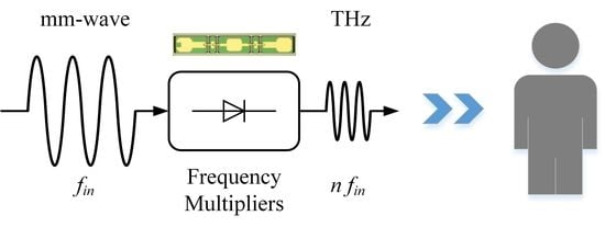
Terahertz (THz) electromagnetic waves have frequencies in the range of 0.1 THz to 10 THz, with corresponding wavelengths of 3 mm to 30 μm. This frequency range is adjacent to millimeter-wave electromagnetic frequencies and infrared light wavelengths, and is thereby associated with the engineering domain of both electromagnetics and photonics. Due to insufficient development and utilization, this frequency is often referred to as a “terahertz gap”. Terahertz-wave technologies have unique properties that include a large-magnitude skin depth, good directivity, wide bandwidth and high imaging resolution [1,2]. Therefore, terahertz-wave technologies possess an unparalleled advantage for remote sensing applications [3,4,5]. Terahertz waves span a wide electromagnetic spectrum and have unprecedented capability for the extraction of information [6,7]. In addition, the THz frequency band covers the vibration and rotation energy spectra of many gas molecules, and the atmospheric trace components of specific chemical species and phase states can be detected from characteristic absorption lines. Terahertz waves are non-ionized and have better penetration ability than infrared light. Therefore, terahertz waves utilized for active remote sensing applications are less attenuated by particles such as dust and smoke, allowing for detection applications related to fire and particulate matter [8]. Compared with microwave remote sensing systems, terahertz imaging devices allow for higher resolution in the context of radar imaging, which is due to the use of shorter wavelengths convenient for the collection of imaging data [9,10,11,12]. Additionally, terahertz waves have good system integration potential for satellite, missile, small UAV (unmanned aerial vehicle) and other robotic platforms due to the use of compact antennas and associated circuits. Terahertz remote sensing technology, therefore, provides an effective means to detect target object information for military and civilian applications. However, stable and energy-efficient terahertz sources have been relatively challenging to develop and terahertz remote sensing technology has taken a long time to engineer and commercialize. Moreover, associated application circuits and systems have not been widely promoted for commercialization. The development of reliable terahertz frequency multipliers with a low cost and small volume at frequencies < 500 GHz has allowed for the more rapid development of innovative and novel remote sensing technologies.
Terahertz remote sensing systems can obtain information related to long-distance targets specified as objects or areal regions, which is accomplished by actively transmitting a terahertz signal or passively detecting terahertz radiation [13,14]. Terahertz remote sensing processing pipelines involve: (1) receiving electromagnetic waves; (2) processing a digitized version of the waveform to obtain remote sensing target entity information; (3) utilizing inverse and forward models to obtain information related to the target. In general, the process of remote sensing is associated with forward and inverse modeling. Forward modeling involves the production of outputs similar to the received waveforms by utilizing a set of parameters as inputs, whereas inverse models utilize the received waveforms to reconstruct a set of parameters that have some physical basis.
Terahertz sensing technology involves active and passive sensors [15,16,17]. Active methods transmit terahertz waves to the target area via an antenna; the reflected terahertz signal is subsequently received to obtain information related to the measured area. Active remote sensing is predominantly used for terahertz radar imaging systems. Radar imaging systems using terahertz-wave technologies have excellent spatial and angular resolution and are resilient to interference and intentional jamming. Passive terahertz remote sensing involves receiving a signal radiated or scattered by an object to obtain target area information. Compared with active remote sensing, passive remote sensing signals contain more information. This is due to blackbody radiation and the Stefan–Boltzmann law, whereby all objects at a temperature above 0 K will produce thermal radiation. Thermal radiation emitted by objects with lower temperatures > 2 K is mostly concentrated in the terahertz band. Therefore, compared with active remote sensing technologies, passive remote sensing signals used for terahertz sensing contain more information.
Active remote sensing is less affected by the radiation of thermal energy from the surrounding environment. Active remote sensing has advantages of high resolutions and longer electromagnetic signal ranges, particularly for imaging systems. However, the design of active remote sensing systems is more complex; active remote sensing systems require a stable and efficient terahertz source; correspondingly, the cost is higher than for passive remote sensing systems. Passive remote sensing systems have simpler designs, do not require terahertz sources, and the costs are correspondingly lower than for active remote sensing systems. For remote sensing and imaging applications, terahertz radiation imaging is conceptually similar to optical imaging, involving the identification of objects. Object identification systems are often designed for outdoor use and strong target object penetration and backscatter, but such systems are affected by the surrounding environment. Due to the low energy magnitude of reflected or emitted terahertz signals received from the target object, terahertz detector circuits are required to have high sensitivity and require careful design to maximize the signal-to-noise ratio (SNR).
Both active and passive terahertz sensors require circuits with design parameters related to conditions of stability and high efficiency. Terahertz remote sensing technology is, therefore, limited by the operation of the terahertz circuitry; this especially involves terahertz frequency multipliers. With the use of Schottky diode-based frequency multiplier sources, terahertz radiation can currently be produced in a stable and low-power fashion. Terahertz sources are often designed using a microwave oscillator circuit coupled with amplification and frequency multiplication circuits utilizing Schottky diodes [18,19]. Therefore, the use of a Schottky diode-based frequency multiplier is an important enabling technology for terahertz remote sensing.
2. Diode Component
2.1. Diode Structure
Before the end of 1980s, whisker Schottky diodes were widely used for the design of terahertz frequency multipliers and mixers owing to their extremely low parasitic parameters (capacitance, resistance and inductance not specified by the design) and simple processing technology associated with the manufacturing process [18]. The small number of parasitic elements is due to the completely vertical structure: this produces the minimum parasitic capacitance between the whisker and the cathode. However, this structure also has major disadvantages. First, the whisker structure is fragile and can be easily damaged. Second, the whisker diode can be difficult to form in a planar fashion. Moreover, the whisker structure cannot be easily mass produced and is associated with a lower yield in mass production.
Since the 1990s, semiconductor manufacturing technology has progressed, and the terahertz Schottky diode is nominally made using a planar structure in lieu of the more traditional whisker structure. In 1987, William L. Bishop proposed a whiskerless Schottky diode with a multilayer planar structure (Figure 1). Although the parasitic capacitance, inductance and dielectric loss of the planar structure deteriorate the high-frequency performance, the planar Schottky diode has the advantages of a stable structure, easy planar integration and good manufacturing consistency. In particular, the adoption of air bridge technology reduces the parasitic parameters. Consequently, planar Schottky diodes quickly replaced whisker diodes in semiconductor manufacturing. The planar Schottky diode has a hierarchical layer structure, as shown in Figure 1; this structure includes a GaAs (Gallium arsenide) substrate, a highly doped GaAs buffer layer, a lightly doped GaAs epitaxial layer, an SiO2 (Silicon dioxide) layer and a metallization pattern layer from bottom to top. The epitaxial layer is lightly doped with a concentration level of ~1017 cm−3 (ranging from 0.5 × 1017 cm−3 to 5 × 1017 cm−3) to form a Schottky contact with the anode, while the buffer layer is heavily doped with a doping level of ~1018 cm−3 (generally 5 × 1018 cm−3) to form a low-resistance transmission channel and good ohmic contact with the metal pad leading out from the cathode of the Schottky diode contacts.
With the development of planar Schottky diodes, some new diode structures have been developed for different applications. The heterojunction barrier diode (HBV) was first invented by Chalmers University of Technology during the early 1990s [20]. The HBV diodes were invented based on harmonic generation in resonant tunneling diodes (RTDs), and were developed from the semiconductor superlattice theory proposed by L. Esaki and R. Tsu [21,22]. The first planar HBV with airbridges was presented by the University of Virginia in 1997 [23]. This design involves even symmetric C-V (capacitance-voltage) characteristics and odd symmetric I-V (current-voltage) characteristics. Therefore, the structure will produce odd harmonics rather than even harmonics, making it suitable for higher-order frequency multipliers [24] (3× [25,26,27], 5× [28] and 7× [29] as three-times, five-times and seven-times).
In order to easily integrate the diode into millimeter and sub-millimeter circuits, a quasi-vertical diode [30] was proposed by researchers at the University of Virginia, with the ohmic contact formed directly below the anode. A comparable or lower series resistance is obtained by the quasi-vertical diode relative to the traditional coplanar diode structure with a similar anode diameter. Through an epitaxial transfer process, the quasi-vertical diode was integrated on a high-resistivity silicon substrate.
In order to enhance the power capacity and resulting output power of the frequency multiplier, different technical design decisions have been adopted to achieve better single-anode power capacity. One of the important technical directions is the use of new semiconductor materials, such as GaN (gallium nitride). The Hebei Semiconductor Research Institute reported on the manufacturing of a series of GaN diodes and measured results from frequency multipliers. GaN is a wide forbidden-band semiconductor material (for example, 3.4 eV), with higher-magnitude electron volts than the traditional GaAs material (for example, 1.42 eV). A diode constructed from GaN material will have a higher reverse breakdown voltage, which means that the diode can withstand greater input power levels. However, one disadvantage of GaN materials is the relatively low electron mobility, which leads to a large series resistance associated with the semiconductor structure. Earlier GaN diodes had series resistance of the order tens of ohms. Through process optimization, the series resistance of GaN diodes has reached an order of 10 ohms, which has greatly improved the cut-off frequency and working frequency band of GaN diodes. For example, a 100 mW output power at a frequency near 300 GHz was attained in pulse-mode operation [31]. The GaN-based Schottky diodes have a similar layer structure to GaAs (gallium arsenide) Schottky diodes. The difference is that the GaN epitaxy is produced on a SiC (silicon carbide) substrate for better lattice matching. Besides changing the semiconductor material, we also presented a novel and patented dual-finger structure that improved the power-handling capability [32].
2.2. Diode Manufacturing
A Schottky diode is a two-terminal device composed of a metal semiconductor junction that forms a barrier to the flow of electrons. The non-linear characteristics of the Schottky diode provided by its junction barrier make the diode an important device for frequency conversion, particularly in the terahertz band. Schottky diodes are reliable non-linear components with good performance and frequency characteristics over the entire terahertz frequency range. The high structural reliability and low (flicker, thermal and shot) noise of Schottky diodes make them suitable for applications that require compact, rugged, low-power and low-noise systems. Moreover, Schottky diodes have good temperature stability and can work well at low temperatures as compared to other diodes (such as silicon switching signal diodes).
The core of the Schottky diode is the metal semiconductor contact (the “Schottky contact”) produced at the anode metal and semiconductor contact surface. Compared with traditional whisker diodes, the high-dielectric materials and planar geometry of planar diodes increase the parasitic effects, which deteriorates the high-frequency performance of these diodes. However, planar Schottky diodes have the advantages of a stable structure, easy planar integration and good consistency. In particular, the adoption of air bridge technology has greatly reduced the parasitic parameters [33]. Figure 2 shows a scanning electron micrograph of a planar Schottky diode with an air bridge structure that consists of the mesa area, ohmic cathode, Schottky anode and interconnected metal formation.
The photolithography process can adequately produce modern planar Schottky diodes; planar diodes have good processing accuracy and process repeatability. For diode structure fabrication, multiple photolithography processes are required. Some photolithography layers have larger pattern sizes, while other layers have smaller pattern sizes. The process level of these smaller pattern photolithography layers usually determines the device performance and yield of the planar diodes; correspondingly, there is a critical layer that affects the device operation. When developing a photolithography process for a new technology node, the non-critical layer can be used with an older technology, while the critical layer can be associated with a new process. As the core process in diode manufacturing, the quality of the photolithography directly affects the performance. Especially in the terahertz band, sub-micron or smaller-sized features are affected by the quality of the lithography process.
The basic process of photolithography can be divided into the following four steps, as shown in Figure 3 and listed below.
- (1)
- In the first step, a photoresistance layer is spin-coated onto the surface of the wafer and dried. Before spin coating, surface hydrophobization is used to improve the adhesion of the wafer surface to the photoresistance layer, which involves vaporized hexamethyldisilazane (HMDS, (CH3)3SiNHSi(CH3)3). HMDS replaces the hydrophilic hydroxide radicals (OH−) on the wafer surface with hydrophobic OSi(CH3)3− for pre-treatment;
- (2)
- In the second step, the dried wafer is exposed in a photolithography machine to stimulate a photochemical reaction. With the development of photolithography technology, the exposure method gradually progresses from a full-silicon exposure to a step-and-repeat exposure and a step-and-scan exposure. The all-silicon 1:1 exposure method is a simpler process and does not require a highly monochromatic light source. However, due to its precision, the step exposure mode has become the de facto method of fabrication due to its reduced magnification exposure mode.
- (3)
- In the third step, the exposed wafer is baked for the second time in a post-exposure baking (PEB) process. The photosensitive elements generated during the exposure process are diffused during baking. The photoresist forms a latent image consistent with the photoresist mask.
- (4)
- Finally, the exposure pattern is developed via spraying or soaking in a developer solution. The developer solution is generally a strong alkaline solution, such as tetra methyl ammonium hydroxide (TMAH, (CH3)4NHO). The latent image is washed away by the developer and the mask pattern is displayed on the photoresistance layer. Another baking cycle can be performed after development to remove the moisture in the photoresistance layer.
During the design and fabrication of the diode, the material system and epitaxial structure of the wafer are the primary considerations that determine performance. GaN-based Schottky diodes can achieve a reverse breakdown voltage of 15 V, and this is useful for high-power frequency multiplier circuits at frequencies of 100 GHz to 300 GHz. InP (indium phosphide) Schottky diodes have a barrier height of 0.2 eV, which makes these devices useful for high-sensitivity detectors. The performance of GaAs-based Schottky diodes falls between the performance of GaN and InP diodes, while GaAs-based designs are the most widely tested terahertz diodes. The diode fabrication technologies used for the different substrate materials are slightly different based on the metal system, annealing temperature and etching method. GaAs-based Schottky diode manufacturing steps are described as an example to illustrate the diode manufacturing process. The diode manufacturing process is mainly carried out in the following five steps.
- (1)
- In the first step, the diode mesa is formed using etching technology (Figure 4b). According to the diode design, the extra epitaxial part outside the mesa can be removed by chemical etching or plasma etching. The chemical corrosion process has the advantages of simplicity and low cost. However, isotropic etching using solution can cause additional lateral corrosion. Plasma etching with anisotropic etching characteristics is a good manufacturing technology for small-sized structures. Chemical etching can directly use the photoresistance layer as a mask. Plasma etching requires the deposition of a layer of oxide film with a high etching selectivity ratio to serve as a mask; the mask is removed after the etching is completed.
- (2)
- The etching method of the diode mesa can be selected according to the design requirements. A thin dielectric film is deposited to achieve passivation of the semiconductor material, as shown in Figure 4c. Depositing a dielectric film on the surface of the epitaxial layer can effectively protect the surface structure of the semiconductor material. Meanwhile, the dielectric film around the anode can reduce the diode leakage effects during circuit operation. Silicon oxide films and silicon nitride films are widely used dielectric films for the diode manufacturing process. The thickness of the dielectric is generally 1000 Å to 2000 Å, while the dielectric film is deposited by thermal oxidation, chemical vapor deposition (CVD) and atomic layer deposition (ALD). Silicon oxide films and silicon nitride films are widely used electrolyte films in the diode manufacturing process.
- (3)
- The diode cathode ohmic contact is formed by etching and metal deposition, as shown in Figure 4d. The ideal ohmic contact is an essential part of the diode. The specific contact ohmic contact resistance Rc is expressed as:where is the barrier height, is the normalized doping concentration, k is the Coulomb constant, T is the absolute temperature, q is the electron charge magnitude, A is the cross-sectional area, is the reduced Planck’s constant, N is the impurity concentration and is the effective mass of the electrons and holes (assumed to be approximately constant near the temperature T). The pi constant is π. Since kT << E00, the field emission (FE) near the Fermi level plays a dominant role during current transport and is associated with a pure tunneling process. A high doping concentration and low barrier height are measures to achieve low ohmic resistance. Using photolithography, the photoresistance layer on the surface of the epitaxial layer appears in a sequence of grooves with the same morphology as the cathode metal. The epitaxial layer at the grooves is removed using etching technology and a highly doped (1 × 10¹⁸–1 × 1019 cm−3) buffer layer is deposited. The ohmic metal layer is using atomic layer deposition (ALD) or radio frequency physical vapor deposition (RFPVD) methods. Annealing can effectively reduce the work required to construct system elements. The Ni/Ge/Au system is used to obtain ohmic contact resistance under annealing conditions. The anode Schottky contact is achieved via metal deposition, as shown in Figure 4e. There is a difference between the work function of the anode metal of the Schottky diode and the Fermi energy of the epitaxial layer. This difference forms a Schottky barrier at the contact surface, and this means the anode current of the Schottky diode is mostly based on thermionic emission (TE). A low metal work function and high epitaxial layer Fermi levels can reduce the height of the Schottky barrier. The thickness of the metal forming the Schottky contact is generally selected to be between 50 Å to 100 Å to obtain a relatively stable work function. Similar to the production of ohmic metal, the photoresistance layer on the surface of the epitaxial layer has grooves with the same morphology as the anode metal. The Ai/Pt/Au metal system can form a Schottky barrier of 0.6 eV to 0.7 eV for the GaAs Schottky diode. Note that the Schottky metal elements are made after the dielectric and ohmic metal elements to avoid barrier reduction of the Schottky metal at high temperatures associated with the process. This is a key breakthrough in ensuring the barrier height of the Schottky junction.
- (4)
- Finally, metal interconnection and pad production are achieved via electroplating, as shown in Figure 4f. The electroplating process generally utilizes a double-layer photoresistance stak. Both layers of photoresistance material have grooves with the same topography as the electroplated metal. A plating seed layer such as Ti/Au (titanium/gold) is deposited using the RFPVD method between two layers of photoresistance material, and this provides an adequate current path for electroplating. An accelerator, suppressor and leveler chemicals are often added to the electroplating solution to improve the leveling of the electroplated metal. After the electroplating, the photoresistance material and the seed layer are etched and removed, and the desired pattern is obtained.
3. Diode Model
The core device that allows the frequency multiplication function of the frequency multiplier circuit is the planar Schottky diode. Therefore, when designing the frequency multiplier circuit, the diode must be accurately modeled. The accuracy of the model will directly affect the performance of the frequency multiplier circuit. The core role of the planar Schottky diode is associated with the intrinsic non-linearity of this circuit element. The parasitic parameters from the structure, packaging and assembly also have an effect on the performance of the diode. Therefore, the modeling of Schottky diodes consists of two parts: one part is the parasitic effect of Schottky diodes in the terahertz frequency band, while the other part is associated with the intrinsic physics-based operation of the Schottky diode.
3.1. Parasitic Models
For the modeling of the parasitic part, an equivalent circuit model is often used in the microwave or lower-frequency bands. The equivalent circuit model establishes a lumped parameter equivalent circuit by combining parasitic parameters with some intrinsic parameters [34]. The parasitic capacitance between the anode pad and the cathode pad is Cpp, and the parasitic capacitance between the mesa and the air bridge is Cfp. The total parasitic capacitance is the sum of the parasitic capacitance of each part as Cptotal = Cpp + Cfp. Lf and Rf are the parasitic capacitance and parasitic inductance introduced by the air bridge. Rj is the Schottky junction resistance, Cj is the Schottky junction capacitance and Rs is the series resistance. These three parameters represent the intrinsic parasitic contributions. In addition, the parasitic inductances Lpad1 and Lpad2 and parasitic capacitances Cpad1 and Cpad2 are also added as associated with the pads.
Although the equivalent circuit model considers the parasitic effects of the diode, this method is limited by the measured frequency range of the diode in an actual functioning remote sensing system. The operating frequency of diodes used in the terahertz frequency band is often higher than the manufacturer’s test frequency range. Therefore, S-parameter test data are often not available for reference. Moreover, the diode is always assembled in a corresponding cavity structure, meaning the equivalent circuit does not take into consideration the parasitic effects of the circuit assembly and cavity structure. Therefore, in the terahertz frequency band, the equivalent circuit model is not completely accurate. Quantifying the influence of the parasitic contributions to the circuit is necessary to explore a more accurate, universal and reliable diode modeling method.
In 1996, Hesler and colleagues proposed a three-dimensional electromagnetic (3D-EM) model of a diode when developing a terahertz harmonic mixer design [35]; the operating physics are applicable to the design of a terahertz frequency multiplier. This modeling method can be used to establish a three-dimensional (3D) electromagnetic model and associated packaging structure related to parasitic contributions to the diode by using 3D-EM simulation software, which involves appropriate characterization of internal and external wave ports, the S-parameter response and characterization of the parasitic contributions to the diode structure and associated circuits. The 3D-EM modeling method has high accuracy, good universality for extension to other related circuit designs and is not limited by theoretical frequency constraints. Therefore, the 3D-EM method is the most commonly used method to characterize parasitic contributions during the design process.
The 3D structure of a planar Schottky diode is shown in Figure 5a. A 3D-EM model can be used to establish an accurate three-dimensional model of the diode with respect to the operating physics and can also be used to set reasonable internal ports at the Schottky junction in the model. Taking the GaAs Schottky diode as an example, the composition dictates the operating response. Since most of commercial 3D-EM field simulation software cannot realistically simulate the doping of semiconductors, an approximate treatment must be made for the buffer layer and epitaxial layer, whereby the heavily doped buffer layer is set as an ideal conductor due to its higher conductivity, and the lightly doped epitaxial layer is set as GaAs due to its lower conductivity.
The Ansys High-Frequency Structure Simulator (HFSS) software that is often used for high-speed designs does not support an internal wave port, so approximate assumptions need to be considered to develop an equivalent model suitable for modeling. The anode probe must be extended to the buffer layer and a coaxial-like wave port must be made slightly larger than the anode column at the interface. The schematic diagram of an internal wave port setting in 3D-EM modeling is shown in Figure 5b [35].
The coaxial probe port (Figure 6) not only simulates the linear part of the diode and the parasitic effects, this port can also provide an interface to connect the linear parasitic part and the non-linear inherent part. However, since only one port is set in the Schottky junction, only the inherent model of the diode at one end can be embedded in the 3D-EM model and the other end is connected to the ground. This model conflicts with the small-signal model shown in Figure 1b, where the intrinsic model of the diode is connected in series between the anode and cathode instead of being connected parallel to the ground.
In order to solve this problem, our team proposed a new type of dual lumped port technology (DLPT) adapted from an existing three-dimensional electromagnetic model [36]. This technology does not require the anode to penetrate the epitaxial layer; only two adjacent rectangular sheets are set in the gap (epitaxial layer) between the anode and buffer layer and the sheets are distributed as lumped ports. As shown in Figure 7a, the two red rectangular regions represent dual lumped ports; the lumped port near the anode represents the anode port and the lumped port near the buffer layer represents the cathode port. Therefore, a relationship between the internal ports of the 3D-EM model and the corresponding internal model ports (Figure 7b) is established. The inherent model of the diode can be naturally embedded into the 3D-EM model, and the micro-coaxial path shown in Figure 6 is no longer needed. The non-physical ground path is required by the MCPT probe technology.
Using the proposed DLPT, a 110 GHz broadband tripler was designed, and the measurement results were compared with the simulation results. This verified the accuracy of the technology.
3.2. Intrinsic Model
The intrinsic part of the Schottky diode is modeled in a traditional fashion by using an equivalent SPICE (Simulation Program with Integrated Circuit Emphasis) model in ADS (Advanced Design System) software. Although this method can adequately model the non-linear region of Schottky diodes as the operating frequency increases, it is challenging to consider effects associated with the diode structure at high frequencies; this includes current saturation, electrothermal, edge and tunneling effects. Therefore, the accuracy of this method is not adequate at higher frequencies and there is a need to also use other modeling techniques.
As early as the 1990s, Kolberg et al. discovered a current saturation effect of Schottky diodes [37]. When the input power to the diode structure increases in the terahertz band, the series resistance of the structure will significantly increase. To verify these findings, they designed a 160 GHz doubler circuit. The verification results showed that when the input power is greater than 20 mW, the series resistance is three times the series resistance of the structure measured at DC conditions; moreover, the simulation and measured results were in good agreement.
In 2016, Diego Moro Melgar et al. applied one-dimensional (1D) drift diffusion and two-dimensional (2D) Monte Carlo models in conjunction with the Harmonic Balance Simulation Tool in ADS to accurately describe the electron transport process of diodes [38]. The researchers used a Monte Carlo method to simulate and analyze the sources of fringe capacitance and determine the static capacitance of Schottky diodes, thereby establishing a capacitance-voltage (C-V) model based on fringe effects and surface states. This method, therefore, provides beneficial theoretical guidance for the design of terahertz frequency multipliers [5].
In 2017, a previous report from our research group proposed a model of a Schottky barrier diode that focuses on the non-linear junction capacitance at terahertz frequencies [39]. An equation that accurately describes the diode characteristics and simulates harmonic balance was derived. The equation was embedded into the SDD (Symbolic Defined Device) control in Atlas simulation software (Silvaco) (Figure 8). In the modeling process, according to the actual physical structure and parameters of the diode, the materials, doping concentrations (such as epitaxial doping 2 × 1017 cm−3) and doping methods are first defined for different regions in the structure established in Atlas. Then, appropriate physical models should be chosen to simulate the carrier transport process, including mobility models (CONMOB and FLDMOB), carrier recombination models (Shockley-Read-Hall), a carrier statistical model (Boltzmann) and a collision ionization model (SELB). Finally, the model was verified for a terahertz high-efficiency frequency 140 GHz doubler. The error between the simulation results and the measured results was reduced by 60% compared to traditional modeling methods.
When the diode is operated at high power levels, it will inevitably generate heat, and heat dissipation and transport in the presence of circuit elements will cause a difference between the measured and modeled diode operation. Conducting research on the thermal effect of diodes in 2011, Kiuru et al. proposed a method to extract the series resistance and thermal resistance of Schottky diodes from S-parameters and I-V characterization measurements. This method avoids the inaccuracy of parameter measurements caused by the temperature rise of the anode junction. This model can more accurately extract the thermal resistance and series resistance of the device under testing (DUT). In the same year, Tang et al. published a study that researched transient and steady-state thermal analyses of planar Schottky diodes at high power [40]. With respect to the method proposed by Tang and colleagues, the thermal model equation is solved using three-dimensional finite element (FE) methods, the temperature-related material characteristics are obtained from the model, and the steady-state and transient thermal characteristics of the frequency multiplier circuit are analyzed. This provides useful information suitable for circuit reliability applications and high-power circuit design and optimization.
In 2014, Carlos et al. [41] conducted a study on the electric heating effect of diode elements. An electrothermal model was linked with a circuit simulator involving harmonic balance technology, thereby providing a tool for designing and analyzing planar Schottky diodes. The authors used a 200 GHz doubler as an example, and by comparing the previous simulation results with actual measurement results, they found an increase in accuracy after thermal effects were considered.
In 2020, Orfao and colleagues analyzed the surface charge effect and fringe capacitance of a planar Schottky diode using a Monte Carlo simulator. The fringe effect parameter β was influenced by the existence of the surface charge on the semiconductor–dielectric interface σ. Subsequent analysis of Schottky diodes within the context of the study found that the edge capacitance effect can be minimized by reducing the value of the lateral extension length of the epitaxial layer. This discovery provided a foundation for improving the performance and power capability of the frequency multiplier [42].
A large amount of research has been performed on the modeling of the Schottky diode. With an increase in operating frequency, the required size of the Schottky diode decreases, and the influence of high-frequency effects on the charge carrier transport process becomes more significant in the design. Physical-based models using drift diffusion or Monte Carlo simulation can accurately describe the behavior of charge carriers at terahertz band frequencies. As the input power increases, an accurate diode model is only achieved when thermal effects are taken into consideration.
In 2021, our group conducted research on an electro-thermal model of the Schottky barrier diode [43]. Using electromagnetic heating multi-physics and coupling heat and electrical current transfer models, we examined the temperature and electrical current distributions of the Schottky diode with respect to different electrical power inputs. The overall temperature distribution of a six-anode Schottky diode is shown by Figure 9. Changes in temperature over the entire structure area are concentrated near the Schottky barrier, which is the region with the most obvious non-linear effects. The current density mode and surface current distribution of the diode anode (excluding the insulating layer and the epitaxial layer) are shown in Figure 10. Most of the electrical current in the diode structure is mainly distributed near the Schottky barrier, where the current flows from the buffer layer to the adjacent ohmic contact. For electrical current heat transfer, the electrical potential and material conductivity in the epitaxial layer of the diode were only used to calculate the power dissipated by the diode structure to determine the effect of dissipated power on diode self-heating. This indicates that the modeled electrical current density of the diode is not equal to the actual current passing through the diode.
Considering the synergistic influence of the temperature, saturation current and series resistance of the diode, here a diode SDD model with self-heating effects is constructed by defining the current and voltage at the input and output ports. The SDD self-heating model includes a temperature-dependent saturation current, the thermal resistance related to the dissipation power, the junction temperature related to the dissipation power and thermal resistance, the dissipation power related to the port current and port voltages. Compared with the diode SPICE model consisting of constant parameters, the current saturation phenomenon is demonstrated by the diode SDD model, and this validates the physical–electro-thermal diode model. Utilizing an electro-thermal model of a Schottky diode based on self-heating effects provides the means for the design and optimization of the Schottky barrier diode and terahertz frequency doubler.
4. Design Methodology of Frequency Multipliers
The adequate design of terahertz frequency multipliers relies on 3D field simulation software and circuit simulation software for electrical field and circuit optimization. Associated with the exploration of the design parameter space, there are three main design methods for terahertz frequency multipliers: the sub-division design method (SDM) based on optimizing the unit circuit design the global design method (GDM) based on optimizing the overall circuit performance and the half-sub-division and half-global design method (HS-HGDM), which provides design trade-offs and eliminates redundant parameters.
The SDM is a more traditional design method. The basic idea is to decompose the circuit structure into models of several sub-circuits with specific functions, which include input and output probe transition structures, an RF filter structure, a bias filter structure and a diode model structure. Then, 3D electrical field simulation software (such as HFSS) is used to design each sub-circuit, and the S parameters of each sub-circuit associated with the optimal design are exported to the circuit simulation software (such as ADS) in the form of a design file (SNP file). Combined with the diode intrinsic SPICE parameters, an overall harmonic balance simulation circuit for frequency multipliers can be designed. The input and output matching design are executed using an ideal transmission line model in ADS. After attaining the overall performance goals, the matching structure is substituted to HFSS, and associated S-parameters are derived in ADS for design verification. Finally, all sub-circuits, matching structures and diode structures are combined to form the frequency multiplier, and the associated S-parameters are derived and verified in ADS. During the SDM process, it is necessary to switch repeatedly between the ADS and HFSS software to achieve optimized frequency performance in the design.
The GDM is a more flexible design method that is suitable for frequency mixers and multipliers [44]. Differing from the SDM described above, the GDM does not design the sub-circuit structures separately, but further decomposes the sub-circuit structures into smaller transmission line units, which include the waveguide, microstrip, step, short-circuit and surface features. After utilizing a field simulation software such as HFSS to extract parameters, the model is rebuilt in the ADS software and the overall harmonic balance simulation and optimization of the frequency multiplication circuit design are performed. Finally, the overall model is obtained from the combination of the sub-circuits and is verified as a whole. The flow of the GDM design method is shown in Figure 11.
The steps and end goal of the SDM are easy to understand and implement, but this method considers the simulation time in the design process; moreover, the optimization space is limited so the final design is not optimal. In contrast, the GDM is not limited to the optimization of sub-circuits; frequency multipliers are associated with simpler transmission line units, and this greatly expands the number of variables and the optimization space. However, although the GDM expands the optimization space, the GDM design process also contributes other issues to the overall design, including variable redundancy. Moreover, some less-important structures are decomposed, and this can result in many redundant variables and a concomitant increase in the calculation and computer processing time required to achieve a viable and efficient design.
To mitigate this design issue, a comprehensive design method (HS-HGDM) combining SDM and GDM was proposed in our previous work [45,46]. The guiding ideology of HS-HGDM is to adopt the GDM for certain circuit structures and the SDM for other circuit structures (Figure 11). For example, the SDM is used for the design of biased filter parts associated with the frequency multipliers, while the GDM is used for the design of circuit transitions between elements and impedance matching. For practical uses, the HS-HGDM has been demonstrated successfully in the design of various frequency multipliers and mixers; the method demonstrates a good balance between controlling the number of variables and expanding the optimization space [47,48].
5. The Development of Terahertz Frequency Multipliers
Research associated with terahertz frequency multipliers closely follows the progress of semiconductor technology. Research on whisker-type Schottky diodes was performed in the 1970s; by the 1990s, planar Schottky diodes appeared and were widely utilized due to their high reliability, easy integration and good consistency with respect to the manufacturing process. These advantages meant wthe whisker-type as gradually replaced diode with the planar-type diode. Combined with hybrid integrated circuit technology, the planar Schottky diode became the mainstream terahertz frequency multiplier technology. After the year 2000, with the development and improvement of new materials and new processes, monolithic microwave integration technology (MMIC) became an important research direction.
The research institutions working on terahertz frequency multipliers include JPL (Jet Propulsion Laboratory) and VDI (Virginia Diodes) in the United States; Teratech in the United Kingdom; Chalmers University of Technology in Sweden; ACST (GmbH) in Germany; the Paris Observatory of France; and some scientific research institutes in China, including Southeast University, University of Electronic Science and Technology of China (UESTC), China Academy of Engineering Physics and the Hebei Semiconductor Research Institute, among others.
For the development of terahertz multipliers, different technologies and approaches have been proposed for achieving higher frequencies and more powerful output responses. Porterfield, Erickson and colleagues at JPL proposed a balanced doubler structure [49], whereby the diodes in an anti-series configuration are placed at a junction between a waveguide and suspended microstrip to provide mode isolation. This structure has been frequently used to design frequency doublers operating at frequencies spanning millimeter waves to 1.5 THz [50,51,52,53]. For greater output power, a series of power-combined doublers have been proposed and demonstrated [30,54,55,56,57,58,59]. In 2018, Siles et al. designed and manufactured a 510 to 560 GHz GaAs Schottky diode power-combined frequency multiplier [59], with an output peak power of 30 mW. Compared with the previously reported frequency doubling technology in the same frequency band, this novel design increases the output source signal by nearly 10 times and the conversion efficiency is 8–9%. The tripler exhibits power synthesis technology and an improved epitaxial structure, and consequently the power processing capacity is significantly improved. The power synthesis technology is significantly different from the previous methods of power synthesis using discrete chip (IC, integrated circuit) technologies, since the power synthesis is achieved by directly combining two output signals on a single chip; this allows better control of the amplitude, phase consistency and symmetry of the synthesis circuit. Such broadband high-power terahertz sources can operate at room temperatures and can also be used as the receiver and local oscillator for terahertz imaging and communication systems.
When operating at a high input power, circuit self-heating effects should be considered, and different modeling methods have been proposed to characterize the temperature rise in the diode structure. These methods include transient current measurements [60], a thermal resistance matrix approach [40] and a physical electro-thermal model [41]. These approaches allow for efficient and stable modeling and prediction of frequency multipliers at high operating temperatures using a harmonic balance simulator. For efficient substrate heat conduction, some substrates with good thermal conductivity have been adopted to increase the heat dissipation capacity of frequency multiplier designs; these substates include AlN (aluminum nitride) [61,62] and a diamond heat spreader [63,64]. The Rutherford Appleton Laboratory (RAL) used substrate transfer technology to transfer a GaAs Schottky varactor to an AlN substrate, and this improved the heat dissipation capacity of the circuit [65]. A 320 GHz frequency multiplier designed by researchers at the RAL. The beam lead technology in the circuit provides the grounding for the diode and also serves as the support for the chip. The output power of the frequency multiplier is ~2 mW between 305 GHz to 340 GHz, while the maximum efficiency at 320 GHz is 13.6%.
Traditionally, many frequency multipliers have been designed using GaAs technology. However, GaN material has a wider forbidden width, and this is associated with the higher breakdown voltage and higher power-handling capability. Therefore, various research studies have been associated with the design and production of GaN-based frequency multipliers [31,66,67,68]. In 2016, Viegas and colleagues designed and manufactured a 160 GHz two-octave device based on a Schottky diode with four anode anti-series structures [69]. The frequency doubler has three ports: an input, output and DC bias port. The reverse short circuit structure at the input is used to suppress the dominant waveguide mode TE10 and the height-reducing waveguide structure is used at the input to suppress waveguide mode TM11. This doubler is used an AlN substrate to provide better heat conduction within the structure. A peak output power of 35 mW has been achieved by the AlN substrate doubler with a 150 mW input power and 23% conversion efficiency.
The design of frequency multipliers requires Schottky diodes and associated passive circuit elements, including waveguide-to-microstrip transitions, impedance matching circuits and filters. If each sub-circuit is designed separately, the whole circuit may be larger than required and less efficient. Therefore, designing a frequency multiplier as one cohesive structure is a good way to alleviate certain challenges during design parameter optimization. In 2013, Guo and colleagues designed a 135 GHz to 150 GHz frequency tripler [70] based on Schottky diodes designed as waveguide resonant filters. In the overall frequency tripler structure, the input signal and output signal of the diode part pass through the input and output probes with waveguide resonant filter structures. Therefore, the corresponding impedance matching is achieved within the filter part, and the conversion from higher-loss planar transmission to a lower-loss high-Q waveguide is achieved. In this design, the resonant waveguide provides filtering, impedance matching and a microstrip-to-waveguide transition. Moreover, the frequency tripler has an unbiased circuit structure, which is more popular for practical use.
The HBV is an important device used to generate terahertz waves. The device has odd harmonics due to having a symmetric C-V curve and anti-symmetric I-V curve [24]. A monolithic HBV-based tripler [26] was demonstrated with a 31 mW peak output power at 282 GHz, and a corresponding minimum conversion loss of 11.6 dB was achieved. The thermal resistance and electrical impedance of the HBV diode were assessed using 3-D FEM simulations (COMSOL Multiphysics) and experimental extraction through DC and S-parameter measurements.
From the perspective of circuit implementation, terahertz monolithic integrated circuits (TMICs) have good process manufacturing consistency compared with hybrid integrated circuits (HIC), thereby avoiding errors associated with manual assembly. At present, the TMIC is nominally utilized for the design of terahertz devices due to the high manufacturing accuracy. Table 1 gives a performance summary and comparison between the state-of-the-art frequency multipliers developed with Schottky diodes and HBVs.
Using the proposed power-combined technology, the frequency multiplier devised by JPL achieves an output power up to ten times the output power of associated counterparts designed by other institutes [71]. Ref. [71] has summarized the power outputs of frequency multiplication sources at the time of publication (2018).
The trend summarized in [71] shows that as the output frequency increases, the output power decreases, although there is a research trend to increase the conversion efficiency and output power at higher frequencies. At present, frequency multiplication sources at lower frequency bands can be sufficient for many designs; indeed, frequency multiplication sources are readily available at frequencies above 1 THz. However, the output power of a terahertz source has a low magnitude, so this is still an active area of research. Compared with a frequency multiplier containing a hybrid integrated structure, the use of a monolithic integrated frequency multiplier in a design can reduce the circuit error and improve the output efficiency. A corresponding thin film process and substrate-free process can also help to reduce transmission loss and improve the conversion efficiency. This is the preferred process technology for the design and fabrication of terahertz frequency multipliers. Moreover, accurate modeling of the design can improve the consistency between simulation and actual circuit tests, providing an effective way to improve the output power of the system.
6. Terahertz Remote Sensing System
This section introduces several classic remote sensing systems involving in concealed weapons detection, space debris warning systems and atmospheric or planetary sensing. Following this, a novel 220 GHz remote sensing system for stand-off imaging applications developed by our group based on the use of frequency multipliers is reported, whereby a 110 GHz LO (local oscillator) driven chain and 220 GHz frequency triplers for a transmitting chain are introduced to the design methodology.
6.1. Remote Sensing Applications
The first terahertz remote sensing system to be introduced was the imaging system developed by the Jet Propulsion Laboratory (JPL) of NASA (USA) with radar ranging capability in the terahertz wave band [72]. Frequency modulation is performed using a K-band synthesizer of a single-phase prime 630 GHz scanning vector imager associated with distortion compensation technology. In the heterodyne receiver associated with the system, the terahertz transmitting source and terahertz local oscillator source are provided by a frequency-doubling chain composed of W-band MMIC (monolithic microwave integrated circuit) power amplifier modules and frequency multipliers. The signal source of the vector measurement system uses a ×36 octave chain and second harmonic down-conversion mixer. Both the signal source and local oscillator generate a signal with a tuning range of 14 GHz to 18 GHz with a pair of microwave synthesizer modules; the signal is then amplified through an MMIC amplifier after passing through a ×6 frequency multiplier. The acquisition of a 600 GHz terahertz source is achieved through a 6-octave chain. Finally, the 630 GHz single-pixel scanned imaging system achieves a range resolution of ~2 cm at a 4 m distance.
In 2010, the Northwest Pacific Laboratory developed a 350 GHz radar system with active, broadband and three-dimensional imaging; they also proposed a high-performance heterodyne receiver coupled with near-diffraction quasi-optical focusing and scanning [73]. The experimental radar system consisted of a transceiver, scanner, quasi-optical focusing system and data acquisition system. The transceiver involved frequency conversion technology composed of a frequency multiplier based on Schottky diode technology and a mixer. When transmitting a terahertz RF signal, the signal is generated by the oscillator and converted into a 14.38 GHz to 14.78 GHz microwave sweep signal via up-conversion; the resulting signal is then amplified 24 times through a frequency-doubling transmission chain and converted into a 345.2 GHz to 354.8 GHz terahertz signal for transmission. When receiving the signal, the mixer at the front end of the receiver is a second harmonic mixer. The frequency doubling chain is required to provide the local oscillator signal for the mixer at the front end of the receiver. This down-converts the received terahertz RF signal into an IF (intermediate frequency) signal, and this is convenient for subsequent subsystems, since the signal can then be digitized and processed at a lower sampling rate.
Terahertz technology also has important applications in space and atmospheric sensing [74]. In 2004, NASA (United States) launched the Aura satellite for earth observation, and two polarized 2.5 THz radiometers were used for detection instruments. In 2007, the European Space Agency (ESA) produced a heterodyne spectrometer and edge detection was used to detect gas components. In 2017, NASA launched IceCube (Earth-1 spacecraft), an experimental 3U cube satellite used to observe fine particles forming ice clouds. At the same time, in China additional research was conducted related to terahertz radiometers, including a satellite-borne terahertz radiometer deployed on the FY-3 polar orbiting meteorological satellite and a microwave radiometer deployed on the FY-4 geostationary orbit satellite.
6.2. Development of a 220 GHz Imaging System
This section focuses on the development of a 220 GHz imaging system by our group. Based on previous work [75], a new 110 GHz frequency tripler with a waveguide-to-microstrip inline transition based on a wedge waveguide iris is introduced here. The overall circuit structure is shown in Figure 12. The fundamental wave is input from a 2.92 mm K-connector and passes through input matching, low-pass filter, diode output matching and output probe phases. The standard rectangular waveguide (WR8) is selected as the output waveguide.
The diode selected for 110 GHz frequency doubling is the double flip-chip Schottky diode DBES105a (UMS, United Monolithic Semiconductors), forming a balanced frequency doubling circuit. The frequency doubling circuit only produces odd harmonics and inhibits even harmonics. Therefore, in the overall circuit, the design of the filter can be omitted to simplify the circuit structure. To prevent the third harmonic signal from leaking to the input port, a low-pass filter for suppressing the third harmonic was designed. The greatest difference between the traditional 110 GHz frequency multiplier and our work [75] is the probe structure. The selected probe structure is a new waveguide-to-microstrip inline transition structure. An ultra-compact U-shaped curved waveguide is formed using a wedge-shaped waveguide iris. The wedge-shaped waveguide iris not only serves as the wide wall of the heightening waveguide of the E-plane probe, but also plays a role in impedance matching and parasitic resonance suppression. At the same time, the microstrip circuit and output waveguide of the frequency multiplier based on the new probe structure are in a straight line; this makes the circuit structure more compact, and the final tripler is thereby more convenient for test installation and connection.
After the passive structure design was completed, a frequency tripler circuit structure was designed using ADS software. The SNP design file from the HFSS software was imported into the corresponding circuit structure and a SPICE model was devised for the simulation. By inputting the parameters of the dual flip chip Schottky diode DBES105a into the SPICE model, the input and output matching structures were simulated and optimized. The optimization objectives were the frequency conversion loss, return loss and output power.
When the 110 GHz triple frequency simulation reached the level of performance required for the engineering design, the circuit was physically assembled. The final test result indicated that when a signal with a power of 100 mW was used to drive the 110 GHz frequency tripler, the average output power in the 90 GHz to 120 GHz frequency band was 3.2 mW, the peak output power was 3.67 mW, and the corresponding conversion efficiency was 2.5–3.6%. Figure 13 shows the physical processing block and measured results of the output power.
The 220 GHz frequency multiplier was designed using an unbalanced circuit topology (Figure 14). The frequency multiplier consists of E-face opening input and output standard copper waveguides, suspended microstrip lines, GaAS Schottky varactor chips and DC bias filters connected by bonding wires. The die is a flip chip placed on a 50-μm-thick quartz substrate. Four anodes of the die are arranged in anti-series for higher power output capacity.
When designing the entire frequency multiplier circuit, the SDM method introduced in Section 4 was adopted. First, the HFSS software was used to simulate the linear part of the frequency tripler. Passive circuits in the design include input probe transition elements, an input low-pass filter, a DC-bias low-pass filter and an output probe transition. When designing the transition structure of the input probe, the input waveguide was appropriately widened to facilitate input matching and to shorten the length of the quartz substrate. To suppress the output of the second harmonic, the output waveguide was reduced in width. The input low-pass filter was used to suppress the propagation of the second and third harmonics generated by the diode and to allow the propagation of the fundamental input wave signal to successive stages. After the HFSS software was used to simulate different parts of the model, simulation results were exported as SNP files. The SNP files were imported into the ADS circuit simulation software, where the transmission line impedance was modified around the diode model to provide for input and output matching. Additionally, the bias voltage of the diode was adjusted. Since there is no physically accurate model of the suspended microstrip line in ADS software, the impedance and phase characteristics of the suspended microstrip line were replaced by an ideal circuit transmission line as an approximation. The impedance step change associated with the suspended microstrip line was represented by a physically accurate model and solved using 3D-EM simulation software (Figure 15).
After completing the design, the tripler was fabricated and measured. The final assembled 220 GHz tripler is shown in Figure 16, with dimensions of 28 mm × 24 mm × 22 mm. The tripler was measured using a W-band power module as an input and an Erickson PM4 mm wave/sub-mm wave power meter. The maximum output power in the output frequency range of 200 GHz to 240 GHz was measured to be 3.5 mW, while the minimum frequency multiplication loss was ~15.0 dB from a 120 mW signal input (Figure 17).
Using the novel terahertz frequency multipliers working at 110 GHz and 220 GHz and a sub-harmonic mixer at 220 GHz with planar Schottky diode technology, a remote sensing front end was developed (Figure 18). For the transmitter channel, the final output power should be reached at around 4 dBm in the 200–240 GHz band for a 5 m detection range according to the radar principle. If the gain of the amplifier is assumed to be 15 dB and the insertion loss of the filter is 1 dB, then the output power of the 220 GHz tripler needs to reach −12 dBm. The transmitter front end is composed of a × 2 × 3 × 3 multiplication chain, whereas the low-frequency amplification and frequency multiplier segments were constructed using commercially available ICs. The last frequency tripler is the 220 GHz tripler developed with four-anode Schottky diodes that converts the 73.3 GHz signal provided by the low-frequency multiplication chain to a 220 GHz signal with a conversion loss of ~14 dB. The PA (power amplifier) was developed with an InP HBT (indium phosphide heterojunction bipolar transistor) 0.25 μm processor, and this amplifier exhibits a gain of 18 dB and a saturation output power of 5 dBm in a flip-substrate technique package [76]. Finally, the generated FMCW (frequency-modulated continuous wave) 200 GHz to 240 GHz terahertz signal is radiated into the air by a horn antenna.
The receiver front end is composed of a LO (local oscillator) × 3 × 3 frequency multiplication chain generating a 110 GHz signal with an output power of 3 mW; this includes the 110 GHz tripler developed using Schottky diodes (Section 5). The 110 GHz tripler was used to drive the 220 GHz sub-harmonic mixer. The reflected terahertz signal was received through a horn antenna followed by a low-noise amplifier (LNA) to amplify the signal amplitude, with an average gain of 16 dB. After filtering with a bandpass filter (insertion loss of 1 dB), the signal is injected into a sub-harmonic mixer and down-converted to an IF (intermediate frequency, 1–3 GHz) signal with a SSB (single sideband) of 9–10 dB. Finally, the IF signal is processed by a baseband platform that includes digitization.
The final established 200 GHz to 240 GHz FMCW terahertz transceiver imaging front end is shown in Figure 19. Figure 19a shows the 220 GHz frequency multiplier transmitter chain, delivering a 200 GHz to 240 GHz FMCW signal through an 18-times frequency multiplication and amplification chain. Figure 19b shows the 220 GHz receiver composed of a 110 GHz LO chain, 220 GHz sub-harmonic mixer, filters and 220 GHz LNA (low-noise amplifier).
The 220 GHz transmitter and receiver were characterized and tested separately before combining the transmitter and receiver into an imaging sensor system. The transmitter delivers an output power of 5.2 dBm across a 200 GHz to 236 GHz range, with a peak output power of 6.5 dBm at 223 GHz (Figure 20). The mixer and LNA were characterized using the Y-factor method and found to exhibit noise temperatures of 2958 K for the mixer and 924 K for the LNA. When the IF of the mixer was fixed to 1 GHz with a sweep source and LO frequencies, an average 7.1 dB double-sideband (DSB) conversion gain was measured for the receiver between 200 GHz and 240 GHz, while the maximum conversion gain was 9.7 dB (Figure 21).
To evaluate the effectiveness of the 220 GHz FMCW remote sensing system, a preliminary test platform was built, and a block diagram of the platform is provided in Figure 22. The transmitted initial signal (11.4 GHz to 12.1 GHz) was generated by a direct digital synthesizer (DDS) chip, then the generated signal was multiplied 18 times to the 205.2 GHz to 217.8 GHz range and radiated into the air using a horn antenna. A secondary reflection mirror was used to focus the THz beam to obtain an image. A person held a 40 cm by 25 cm metal plate in front of their chest and stood 5 m away from the horn antenna (Figure 23). The reflected signal detected by the received antenna was converted into an IF signal and digitized using a custom-designed digital signal process (DSP) subsystem. As shown in Figure 23, the image of the 220 GHz remote sensing system in the spatial vicinity of the metal plate shows a significant brightness difference between the metal plate, the surrounding clothing and human body tissue.
7. Conclusions
This paper reviews the development of Schottky-based terahertz frequency multipliers for a terahertz remote sensing system. The review includes diode manufacturing, circuit modeling, design methodology and circuit integration in a remote sensing system. Different technologies and approaches related to material and circuit topology were proposed and verified to obtain a high output power and high-frequency operation for an application circuit and associated remote sensing system. Models associated with 3-D EM, electro-thermal and electrical drift–diffusion processes helped to improve the accuracy when characterizing the parasitic and intrinsic aspects of Schottky diodes in the terahertz band. Several classic terahertz remote sensing systems were reviewed. A 220 GHz remote sensing system established using our novel frequency multipliers was also introduced as well. These technologies and innovations can support the engineering development of terahertz multipliers and promote the practical application of terahertz technology in remote sensing, high-speed communication and radio astronomy.
Author Contributions
Y.Z. and C.W. wrote the manuscript with support from all authors. X.L., L.W., C.D., J.C., Y.L. and N.K. have read and agreed to the published version of the manuscript. All authors have read and agreed to the published version of the manuscript.
Funding
The authors would glad to thank National Natural Science Foundation of China (Grant No. 61871072) for its support of this project.
Data Availability Statement
The data presented in this study are available on request from the corresponding author.
Conflicts of Interest
The authors declare no conflict of interest.
References
- Siegel, P.H. Terahertz technology. IEEE Trans. Microw. Theory Tech. 2002, 50, 910–928. [Google Scholar] [CrossRef]
- Song, H.; Nagatsuma, T. Present and Future of Terahertz Communications. IEEE Trans. Terahertz Sci. Technol. 2011, 1, 256–263. [Google Scholar] [CrossRef]
- Woolard, D.L.; Brown, R.; Pepper, M.; Kemp, M. Terahertz Frequency Sensing and Imaging: A Time of Reckoning Future Applications? IEEE 2005, 93, 1722–1743. [Google Scholar] [CrossRef]
- Dong, P.; Liu, L.; Li, S.; Hu, S.; Bu, L. Application of M5 Model Tree in Passive Remote Sensing of Thin Ice Cloud Microphysical Properties in Terahertz Region. Remote Sens. 2021, 13, 2569. [Google Scholar] [CrossRef]
- Hosako, I.; Sekine, N.; Patrashin, M.; Saito, S.; Fukunaga, K.; Kasai, Y.; Baron, P.; Seta, T.; Mendrok, J.; Ochiai, S.; et al. At the Dawn of a New Era in Terahertz Technology. IEEE 2007, 95, 1611–1623. [Google Scholar] [CrossRef]
- Wells, J. Faster than fiber: The future of multi-G/s wireless. IEEE Microw. Mag. 2009, 10, 104–112. [Google Scholar] [CrossRef]
- Han, R.; Zhang, Y.; Kim, Y.; Zhang, Y.M.; Kim, Y.; Kim, D.Y.; Shichijo, H.; Afshari, E.; Kenneth, K.O. Active terahertz imaging using Schottky diodes in CMOS: Array and 860-GHz pixel. IEEE J. Solid-State Circuits 2013, 48, 2296–2308. [Google Scholar] [CrossRef]
- Zhan, H.; Li, Q.; Zhao, K.; Zhang, L.W.; Zhang, Z.W.; Zhang, C.L.; Xiao, L.Z. Evaluating PM2.5 at a Construction Site Using Terahertz Radiation. IEEE Trans. Terahertz Sci. Technol. 2015, 5, 1028–1034. [Google Scholar] [CrossRef]
- Liu, H.B.; Zhong, H.; Karpowicz, N.; Chen, Y.; Zhang, X.C. Terahertz Spectroscopy and Imaging for Defense and Security Applications. IEEE 2007, 95, 1514–1527. [Google Scholar] [CrossRef]
- Fan, L.; Zeng, Y.; Yang, Q.; Wang, H.Q.; Deng, B. Fast and High-Quality 3-D Terahertz Super-Resolution Imaging Using Lightweight SR-CNN. Remote Sens. 2021, 13, 3800. [Google Scholar] [CrossRef]
- Li, H.; Li, C.; Wu, S.; Zheng, S.; Fang, G.Y. Adaptive 3D Imaging for Moving Targets Based on a SIMO InISAR Imaging System in 0.2 THz Band. Remote Sens. 2021, 13, 782. [Google Scholar] [CrossRef]
- Federici, J.F.; Schulkin, B.; Huang, F.; Gary, D.; Barat, R.; Oliveira, F.; Zimdars, D. THz imaging and sensing for security applications—Explosives, weapons and drugs. Semicond. Sci. Technol. 2005, 20, S266. [Google Scholar] [CrossRef]
- Goossens, S.; Navickaite, G.; Monasterio, C.; Gupta, S.; Piqueras, J.J.; Perez, R.; Burwell, G.; Nikitskiy, I.; Lasanta, T. Broadband image sensor array based on graphene–CMOS integration. Nat. Photon. 2017, 11, 366–371. [Google Scholar] [CrossRef]
- Liu, J.; Dai, J.; Chin, S.L.; Zhang, X.C. Broadband terahertz wave remote sensing using coherent manipulation of fluorescence from asymmetrically ionized gases. Nat. Photon. 2010, 4, 627–631. [Google Scholar] [CrossRef]
- Saeedkia, D. Handbook of Terahertz Technology for Imaging, Sensing and Communications; Elsevier: Aalborg, Denmark, 2013. [Google Scholar]
- Cooper, K.B.; Dengler, R.J.; Chattopadhyay, G.; Schlecht, E.; Gill, J.; Skalare, A.; Mehdi, I.; Siegel, P.H. A High-Resolution Imaging Radar at 580 GHz. IEEE Microw. Wirel. Compon. Lett. 2008, 18, 64–66. [Google Scholar] [CrossRef]
- Chan, W.L.; Charan, K.; Takhar, D.; Kelly, K.F.; Baraniuk, R.G.; Mittleman, D.M. A single-pixel terahertz imaging system based on compressed sensing. Appl. Phys. Lett. 2008, 93, 121105. [Google Scholar] [CrossRef] [Green Version]
- Crowe, T.W.; Bishop, W.L.; Porterfield, D.W.; Hesler, J.L.; Weikle, R.M. Opening the terahertz window with integrated diode circuits. IEEE J. Solid-State Circuits 2005, 40, 2104–2110. [Google Scholar] [CrossRef]
- Chattopadhyay, G. Technology, Capabilities, and Performance of Low Power Terahertz Sources. IEEE Trans. Terahertz Sci. Technol. 2011, 1, 33–53. [Google Scholar] [CrossRef]
- Gronqvist, H.R.; Kollberg, E. Millimeter- and submillimeter-wave multipliers using quantum-barrier-varactor (QBV) diodes. IEEE Electron Device Lett. 1990, 11, 373–375. [Google Scholar] [CrossRef]
- Esaki, L.; Tsu, R. Superlattice and Negative Differential Conductivity in Semiconductors. IBM J. Res. Dev. 1970, 14, 61–65. [Google Scholar] [CrossRef]
- Esaki, L. Discovery of the tunnel diode. IEEE Trans. Electron Devices 1976, 23, 644–647. [Google Scholar] [CrossRef]
- Jones, J.R.; Bishop, W.L.; Jones, S.H.; Tait, G.B. Planar multibarrier 80/240-GHz heterostructure barrier varactor triplers. IEEE Trans. Microw. Theory Tech. 1997, 45, 512–518. [Google Scholar] [CrossRef]
- Stake, J.; Malko, A.; Bryllert, T.; Vukusic, J. Status and Prospects of High-Power Heterostructure Barrier Varactor Frequency Multipliers. IEEE 2017, 105, 1008–1019. [Google Scholar] [CrossRef] [Green Version]
- Vukusic, J.; Bryllert, T.; Emadi, T.A.; Sadeghi, M.; Stake, J. A 0.2-W Heterostructure Barrier Varactor Frequency Tripler at 113 GHz. IEEE Electron Device Lett. 2007, 28, 340–342. [Google Scholar] [CrossRef] [Green Version]
- Vukusic, J.; Bryllert, T.; Olsen, Ø.; Hanning, J.; Stake, J. Monolithic HBV-Based 282-GHz Tripler with 31-mW Output Power. IEEE Electron Device Lett. 2012, 33, 800–802. [Google Scholar] [CrossRef]
- Dahlbäck, R.; Vukusic, J.; Weikle, R.M.; Stake, J. A Tunable 240–290 GHz Waveguide Enclosed 2-D Grid HBV Frequency Tripler. IEEE Trans. Terahertz Sci. Technol. 2016, 6, 503–509. [Google Scholar] [CrossRef]
- Olsen, A.; Ingvarson, M.; Alderman, B.; Stake, J. A 100-GHz HBV frequency quintupler using microstrip elements. IEEE Microw. Wirel. Compon. Lett. 2004, 14, 493–495. [Google Scholar] [CrossRef]
- Qun Xiao, J.L.; Hesler, D.Y.; Crowe, T.W.; Weikle, R.M. A 300-GHz heterostructure barrier varactor (HBV) frequency septupler. In Proceedings of the 2005 Joint 30th International Conference on Infrared and Millimeter Waves and 13th International Conference on Terahertz Electronics, Williamsburg, VA, USA, 19–23 September 2005; pp. 80–81. [Google Scholar] [CrossRef]
- Alijabbari, N.; Bauwens, M.F.; Weikle, R.M. Design and Characterization of Integrated Submillimeter-Wave Quasi-Vertical Schottky Diodes. IEEE Trans. Terahertz Sci. Technol. 2015, 5, 73–80. [Google Scholar] [CrossRef]
- Zhang, L.; Liang, S.X.; Lv, Y.J.; Yang, D.B.; Fu, X.C.; Song, X.B.; Gu, G.D.; Xu, P.; Guo, Y.M.; Bu, A.M.; et al. High-Power 300 GHz Solid-State Source Chain Based on GaN Doublers. IEEE Electron Device Lett. 2021, 42, 1588–1591. [Google Scholar] [CrossRef]
- Yong, Z.; Chengkai, W.; Wei, J.; Bo, Y.; Ruimin, X. A planar Schottky diode with multi finger structure. China ZL 2019, 1133, 4949. [Google Scholar]
- Jelenski, A.; Grub, A.; Krozer, V.; Hartnagel, H.L. New approach to the design and the fabrication of THz Schottky barrier diodes. IEEE Trans. Microw. Theory Technol. 1993, 41, 549–557. [Google Scholar] [CrossRef]
- Tang, A.Y.; Drakinskiy, V.; Yhland, K.; Stenarson, J.; Bryllert, T.; Stake, J. Analytical Extraction of a Schottky Diode Model from Broadband S-Parameters. IEEE Trans. Microw. Theory Tech. 2013, 61, 1870–1878. [Google Scholar] [CrossRef]
- Hesler, J. Planar Schonly Diodes in Submillimeter Wavelength Waveguide Receivers. Ph.D. Thesis, University of Virginia, Virginia, VA, USA, January 1996. [Google Scholar]
- Wu, C.; Zhang, Y.; Xu, Y.; Bo, Y.; Xu, R. Dual Lumped Ports Technique and Its Applications in Modeling of Planar Schottky Diode in THz Band. IEEE Access 2020, 8, 38001–38009. [Google Scholar] [CrossRef]
- Kolberg, E.L.; Tolmunen, T.J.; Frerking, M.A.; East, J.R. Current saturation in submillimeter-wave varactors. IEEE Trans. Microw. Theory Tech. 1992, 40, 831–838. [Google Scholar] [CrossRef]
- Moro-Melgar, D.; Maestrini, A.; Treuttel, J.; Gatilova, L.; Gonzalez, T.; Vasallo, B.G.; Mateos, J. Monte Carlo Study of 2-D Capacitance Fringing Effects in GaAs Planar Schottky Diodes. IEEE Trans. Electron Devices 2016, 63, 3900–3907. [Google Scholar] [CrossRef]
- Renl, T.; Zhang, Y. A study of the terahertz C-V characteristic of the Schottky barrier diode. In Proceedings of the 2017 IEEE MTT-S International Microwave Symposium (IMS), Honololu, HI, USA, 4–9 June 2017. [Google Scholar] [CrossRef]
- Tang, A.Y.; Schlecht, E.; Lin, R.; Chattopadhyay, G.; Lee, C.; Gill, J.; Mehdi, I.; Stake, J. Electro-Thermal Model for Multi-Anode Schottky Diode Multipliers. IEEE Trans. Terahertz Sci. Technol. 2012, 2, 290–298. [Google Scholar] [CrossRef] [Green Version]
- Pérez-Moreno, C.G.; Grajal, J. Physical Electro-Thermal Model for the Design of Schottky Diode-Based Circuits. IEEE Trans. Terahertz Sci. Technol. 2014, 4, 597–604. [Google Scholar] [CrossRef]
- Orfao, B.; Vasallo, B.G.; Moro-Melgar, D.; Pérez, S.; Mateos, J.; González, T. Analysis of Surface Charge Effects and Edge Fringing Capacitance in Planar GaAs and GaN Schottky Barrier Diodes. IEEE Trans. Electron Devices 2020, 67, 3530–3535. [Google Scholar] [CrossRef]
- Cui, J.; Zhang, Y.; Wei, H.; Wu, Q.; Mao, S.; Xu, Y.; Yan, B.; Xu, R. Electro-Thermal Model for Schottky Barrier Diode Based on Self-Heating Effect. In Proceedings of the IEEE the 4th International Conference on Electronics and Communication Engineering (ICECE), Xi’an, China, 17–19 December 2021. [Google Scholar]
- Cui, J.; Zhang, Y.; Xia, D.J.; Xu, Y.H.; Xiao, F.; Yan, B.; Xu, R.M. A 220 GHz Broadband Sub-Harmonic Mixer Based on Global Design Method. IEEE Access 2019, 7, 30067–30078. [Google Scholar] [CrossRef]
- Chengkai, W. Research on Terahertz Frequency Multiplication Technology Based on Schottky Diode; University of Electronic Science and Technology: Sichuan, China, 2018. [Google Scholar]
- Cui, J.; Wei, H.; Huang, S.; Xie, J.; Li, Y.; Yu, C.; Wang, L.; Zhang, Y. Design of a 270–290 GHz frequency tripler based on the Half-Subdivision and Half-Global Design Method. In Proceedings of the International Conference on Microwave and Millimeter Wave Technology (ICMMT), Nanjing, China, 23–26 May 2021; pp. 1–3. [Google Scholar] [CrossRef]
- Cui, J.; Zhang, Y.; Xu, Y.; Ye, L.; Xiao, F.; Yan, B.; Cui, R. A 200–240 GHz Sub-Harmonic Mixer Based on Half-Subdivision and Half-Global Design Method. IEEE Access 2020, 8, 33461–33470. [Google Scholar] [CrossRef]
- Wu, C.; Zhang, Y.; Long, M.; Xu, Y.; Xu, R. Design of a 110 GHz broadband frequency tripler using planar varistor Schottky diodes. In Proceedings of the IEEE MTT-S International Wireless Symposium (IWS), Guangzhou, China, 19–22 May 2019; pp. 1–3. [Google Scholar] [CrossRef]
- Porterfield, D.W.; Crowe, T.W.; Bradley, R.F.; Erickson, N.R. A high-power fixed-tuned millimeter-wave balanced frequency doubler. IEEE Trans. Microw. Theory Tech. 1999, 47, 419–425. [Google Scholar] [CrossRef]
- Wu, C.; Zhang, Y.; Cui, J.; Li, Y.K.; Xu, Y.H.; Xu, R.M. A 135–190 GHz Broadband Self-Biased Frequency Doubler using Four-Anode Schottky Diodes. Micromachines 2019, 10, 277. [Google Scholar] [CrossRef] [PubMed] [Green Version]
- Viegas, C.; Powell, J.; Liu, H.R.; Sanghera, H.; Donoghue, L.; Huggard, P.G.; Alderman, B. On-Chip Integrated Backshort for Relaxation of Machining Accuracy Requirements in Frequency Multipliers. IEEE Microw. Wirel. Compon. Lett. 2021, 31, 188–191. [Google Scholar] [CrossRef]
- Yang, F. Discrete Schottky diodes based terahertz frequency doubler for planetary science and remote sensing. Microw. Opt. Technol. Lett. 2017, 59, 966–970. [Google Scholar] [CrossRef]
- Chattopadhyay, G.; Schlecht, E.; Ward, J.S.; Gill, J.J.; Javadi, H.H.S.; Maiwald, F.; Medhi, I. An all-solid-state broad-band frequency multiplier chain at 1500 GHz. IEEE Trans. Microw. Theory Tech. 2004, 52, 1538–1547. [Google Scholar] [CrossRef]
- Viegas, C.; Liu, H.R.; Powell, J.; Sanghera, H.; Whimster, A.; Donoghue, L.; Huggard, P.G.; Alderman, B. A 180-GHz Schottky Diode Frequency Doubler with Counter-Rotated E-Fields to Provide In-Phase Power-Combining. IEEE Microw. Wirel. Compon. Lett. 2018, 28, 518–520. [Google Scholar] [CrossRef]
- Dou, J.; Jiang, S.; Xu, J.; Wang, W.B. Design of D-band frequency doubler with compact power combiner. Electron. Lett. 2017, 53, 478–480. [Google Scholar] [CrossRef]
- Siles, J.V.; Maestrini, A.; Alderman, B.; Davies, S.; Wang, H.; Treuttel, J.; Leclerc, E.; Narhi, T.; Goldstein, C. A Single-Waveguide In-Phase Power-Combined Frequency Doubler at 190 GHz. IEEE Microw. Wirel. Compon. Lett. 2011, 21, 332–334. [Google Scholar] [CrossRef]
- Maestrini, A.; Ward, J.S.; Tripon-Canseliet, C.; Gill, J.J.; Lee, C.; Javadi, H.; Attopadhyay, G.C.; Mehdi, I. In-Phase Power-Combined Frequency Triplers at 300 GHz. IEEE Microw. Wirel. Compon. Lett. 2008, 18, 218–220. [Google Scholar] [CrossRef]
- Ding, J.Q.; Maestrini, A.; Gatilova, L.; Shi, S.C. High Efficiency and Powerful 260–340 GHz Frequency Doublers based on Schottky Diodes. In Proceedings of the XXXIIIrd General Assembly and Scientific Symposium of the International Union of Radio Science, Rome, Italy, 29 August–5 September 2020; pp. 1–4. [Google Scholar] [CrossRef]
- Siles, J.V.; Cooper, K.; Lee, C.; Lin, R.; Chattopadhyay, G.; Mehdi, I. A Compact Room-Temperature 510–560 GHz Frequency Tripler with 30-mW Output Power. In Proceedings of the 15th European Radar Conference (EuRAD), Madrid, Spain, 26–28 September 2018; pp. 333–336. [Google Scholar] [CrossRef]
- Khanal, S.; Kiuru, T.; Tang, A.Y.; Saber, M.A.; Mallat, J.; Stake, J.; Narhi, T.; Raisanen, A.V. Thermal characterization of THz Schottky diodes using transient current measurements. IEEE Trans. Terahertz Sci. Technol. 2014, 4, 267–276. [Google Scholar] [CrossRef]
- Xiao, Q.; Hesler, J.L.; Crowe, T.W.; Weikle, R.M.; Duan, Y.W.; Deaver, B.S. High-efficiency heterostructure-barrier-varactor frequency triplers using AlN substrates. In Proceedings of the IEEE MTT-S International Microwave Symposium Digest, Long Beach, CA, USA, 17 June 2005; pp. 443–446. [Google Scholar]
- Chen, Z.; Wang, H.; Alderman, B.; Huggard, P.; Zhang, B.; Fan, Y. 190 GHz high power input frequency doubler based on Schottky diodes and AlN substrate. IEICE Electron. Express 2016, 13, 20160981. [Google Scholar] [CrossRef] [Green Version]
- Lee, C.; Ward, J.; Lin, R.; Schlecht, E.; Chattopadhyay, G.; Gill, J.; Thomas, B.; Maestrini, A.; Mehdi, I.; Siegel, P. A wafer-level diamond bonding process to improve power handling capability of submillimeter-wave Schottky diode frequency multipliers. In Proceedings of the 2009 IEEE MTT-S International Microwave Symposium Digest, Boston, MA, USA, 7–12 June 2009; Volume 45, pp. 957–960. [Google Scholar]
- Lee, C.; Ward, J.; Lin, R.; Schlecht, E.; Chattopadhyay, G.; Gill, J.; Thomas, B.; Maestrini, A.; Mehdi, I.; Siegel, P. Diamond heat spreaders for submillimeter-wave gas Schottky diode frequency multipliers. Int. Symp. Space Terahertz Technol. 2009, 2009, 43–46. [Google Scholar]
- Alderman, B.; Manju, H.; Hoshiar, S.; Hui, W.; Simon, R.; Brian, E.; Peter, d.M. Schottky diode technology at Rutherford Appleton Laboratory. In Proceedings of the IEEE International Conference on Microwave Technology and Computational Electromagnetics, Beijing, China, 22–25 May 2011; pp. 4–6. [Google Scholar]
- Liang, S.; Song, X.; Zhang, L.; Lv, Y.J.; Wang, Y.G.; Wei, B.H.; Guo, Y.M.; Gu, G.D.; Wang, B.; Cai, S.J.; et al. A 177–183 GHz high-power GaN-based frequency doubler with over 200 mW output power. IEEE Electron Device Lett. 2020, 41, 669–672. [Google Scholar] [CrossRef]
- Liang, S.; Fang, Y.; Xing, D.; Zhang, Z.R.; Wang, J.L.; Guo, H.Y.; Zhang, L.S.; Gu, G.D.; Feng, Z.H. GaN planar Schottky barrier diode with cut-off frequency of 902 GHz. Electron. Lett. 2016, 52, 1408–1410. [Google Scholar] [CrossRef]
- Min, Y.; Zhang, B.; Fan, Y.; Liang, X.S.; Xing, D.; Wang, J.L. The design of 110GHz frequency tripler using GaN-based planar Schottky diodes. In Proceedings of the IEEE 9th UK-Europe-China Workshop on Millimetre Waves and Terahertz Technologies (UCMMT), Liverpool, UK, 5–7 September 2016; pp. 92–93. [Google Scholar]
- Viegas, C.; Alderman, B.; Pérez-Moreno, C.G.; Powell, J.; Duff, C.I.; Sloan, R. Design and thermal analysis of a high-power frequency doubler at 160 GHz. In Proceedings of the 2016 IEEE MTT-S International Microwave and RF Conference (IMaRC), New Delhi, India, 5–9 December 2016. [Google Scholar] [CrossRef]
- Guo, C.; Shang, X.B.; Lancaster, M.J.; Xu, J.; Powell, J.; Wang, H.; Alderman, B.; Huggard, P.G. A 135–150-GHz Frequency Tripler with Waveguide Filter Matching. IEEE Trans. Microw. Theory Tech. 2018, 66, 4608–4616. [Google Scholar] [CrossRef]
- Siles, J.V.; Cooper, K.B.; Lee, C.; Lin, R.H.; Chattopadhyay, G.; Mehdi, I. A New Generation of Room-Temperature Frequency-Multiplied Sources with up to 10× Higher Output Power in the 160-GHz–1.6-THz Range. IEEE Trans. Terahertz Sci. Technol. 2018, 8, 596–604. [Google Scholar] [CrossRef]
- Dengler, R.J.; Cooper, K.B.; Chattopadhyay, G.; Mehdi, I.; Siegel, P.H. 600 GHz Imaging Radar with 2 cm Range Resolution. Int. Microw. Symp. IEEE 2017, 54, 47–50. [Google Scholar]
- Sheen, D.M.; Hall, T.E.; Severtsen, R.H.; Mcmakin, D.L.; Valdez, P. Standoff concealed weapon detection using a 350-GHz radar imaging system. SPIE Int. Soc. Opt. Eng. 2017, 7670, 115–118. [Google Scholar]
- Liu, F.; Cui, W.; Zhu, Z.; Dong, S.; Shang, S.; Yao, Z. The spaceborne terahertz remote sensing techniques. IET Int. Radar Conf. 2013, 2013. 32, 54–58. [Google Scholar]
- Wu, C.; Zhang, Y.; Li, Y.; Zhu, H.; Xiao, F.; Yan, B.; Xu, R. Millimeter-Wave Waveguide-to-Microstrip Inline Transition Using a Wedge-Waveguide Iris. IEEE Trans. Microw. Theory Tech. 2022, 70, 1087–1096. [Google Scholar] [CrossRef]
- Zhang, Y.; Li, Y.; Chen, Y.; Zhu, H. The development of the package of the Terahertz integrated circuits. In Proceedings of the IEEE Asia-Pacific Microwave Conference (APMC), Marina Bay Sands, Singapore, 10–13 December 2019; pp. 625–627. [Google Scholar] [CrossRef]
Figure 1.
(a) Microphotograph of planar Schottky diode. (b) Equivalent parasitic parameters.

Figure 2.
Scanning electron micrograph of a lithographically defined Schottky diode.

Figure 3.
The basic process of lithography.

Figure 4.
Schematic of the diode fabrication process for Schottky diodes. (a) Epitaxial preparation; (b) Mesa etching; (c) Passivation; (d) Making ohmic contact; (e) Making Schottky contact; (f) Making metal finger.
Figure 4.
Schematic of the diode fabrication process for Schottky diodes. (a) Epitaxial preparation; (b) Mesa etching; (c) Passivation; (d) Making ohmic contact; (e) Making Schottky contact; (f) Making metal finger.

Figure 5.
(a) A 3D structure model of a planar Schottky diode. (b) Schematic diagram of internal wave port setting [35].
Figure 5.
(a) A 3D structure model of a planar Schottky diode. (b) Schematic diagram of internal wave port setting [35].

Figure 6.
A 3-D EM model of a diode based on MCPT (port 3 represents a coaxial probe port; the SNP file is a model design file in TouchStone file format).
Figure 6.
A 3-D EM model of a diode based on MCPT (port 3 represents a coaxial probe port; the SNP file is a model design file in TouchStone file format).

Figure 7.
DLPT and diode embedding method [36]: (a) cross-sectional view of DLPT (red rectangle sheets represent lumped ports with integrated line pointing to each other); (b) 3-D EM model of diode based on DLPT (ports 3 and 4 represent dual lumped ports).
Figure 7.
DLPT and diode embedding method [36]: (a) cross-sectional view of DLPT (red rectangle sheets represent lumped ports with integrated line pointing to each other); (b) 3-D EM model of diode based on DLPT (ports 3 and 4 represent dual lumped ports).

Figure 8.
Physics-based Schottky junction model in Atlas.

Figure 9.
The overall temperature distribution of the Schottky diode (the temperature scale represents the absolute temperature in kelvins).
Figure 9.
The overall temperature distribution of the Schottky diode (the temperature scale represents the absolute temperature in kelvins).

Figure 10.
The current density distribution of the diode anode.

Figure 11.
(a) SDM method based on circuit units and (b) GDM method based on transmission line (TL) units.
Figure 11.
(a) SDM method based on circuit units and (b) GDM method based on transmission line (TL) units.

Figure 12.
Circuit diagram of 110 GHz tripler with new probe structure [75].
Figure 12.
Circuit diagram of 110 GHz tripler with new probe structure [75].

Figure 13.
(a) The physical processing block and (b) measured conversion efficiency of 110 GHz frequency tripler with input power of 100 mW [75].
Figure 13.
(a) The physical processing block and (b) measured conversion efficiency of 110 GHz frequency tripler with input power of 100 mW [75].

Figure 14.
Schematic of the 220 GHz tripler circuit.

Figure 15.
HFSS overall model and ADS overall circuit.

Figure 16.
The picture of 220 GHz frequency tripler.

Figure 17.
(a) Output power at fixed 100 mW power rate. (b) Conversion loss at fixed 100 mW power.

Figure 18.
Block diagram of the developed 200–240 GHz FMCW terahertz remote sensing system for security check applications: (a) transmitter; (b) receiver.
Figure 18.
Block diagram of the developed 200–240 GHz FMCW terahertz remote sensing system for security check applications: (a) transmitter; (b) receiver.

Figure 19.
Photograph of the fabricated 200–240 GHz remote sensing system for imaging applications: (a) transmitter channel; (b) receiver channel.
Figure 19.
Photograph of the fabricated 200–240 GHz remote sensing system for imaging applications: (a) transmitter channel; (b) receiver channel.

Figure 20.
Output power of the 220 GHz transmitter.

Figure 21.
Output power of the 220 GHz transmitter.

Figure 22.
Schematic diagram of the 220 GHz remote sensing imager.

Figure 23.
Imaging results of the 220 GHz terahertz front end for a 5 m stand-off distance.


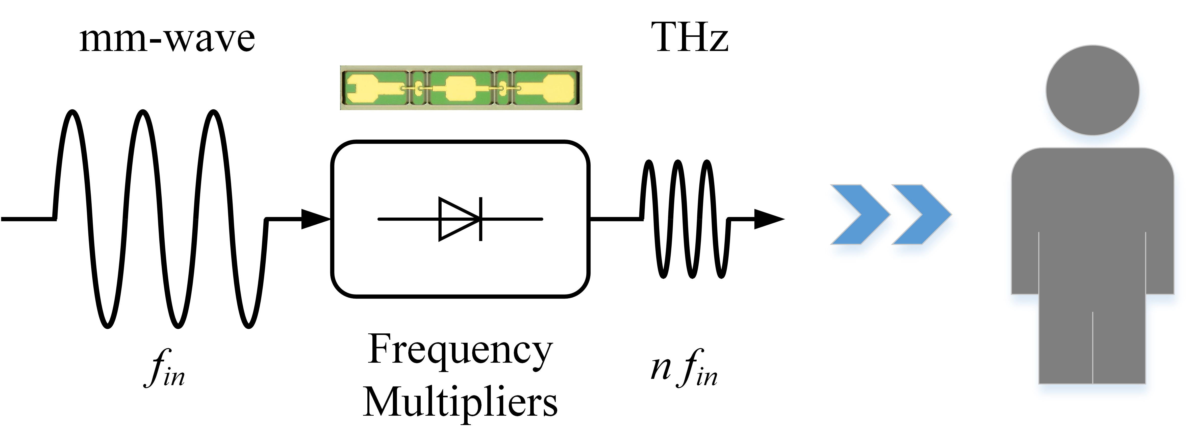
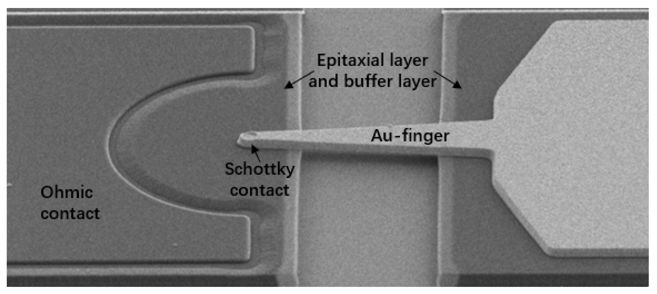
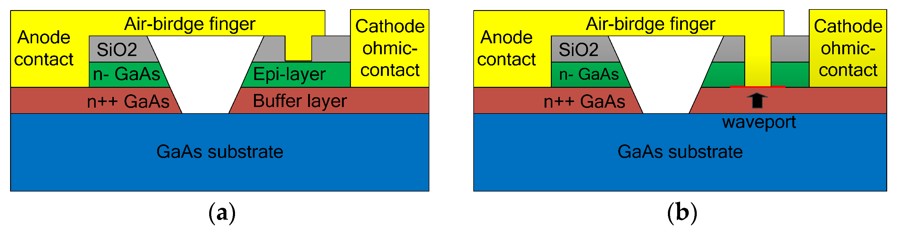
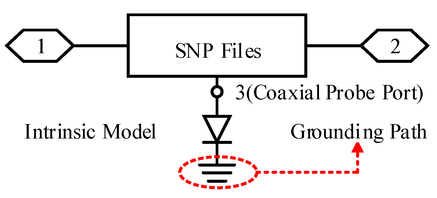
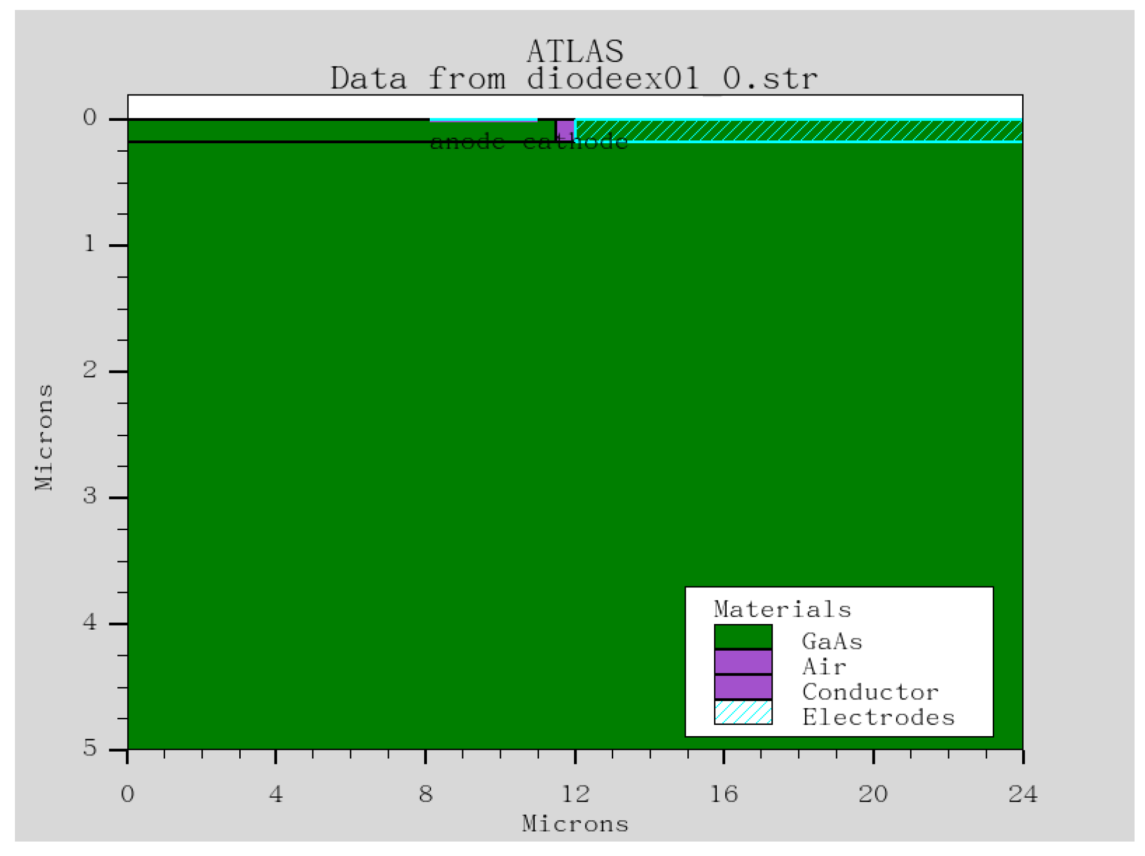
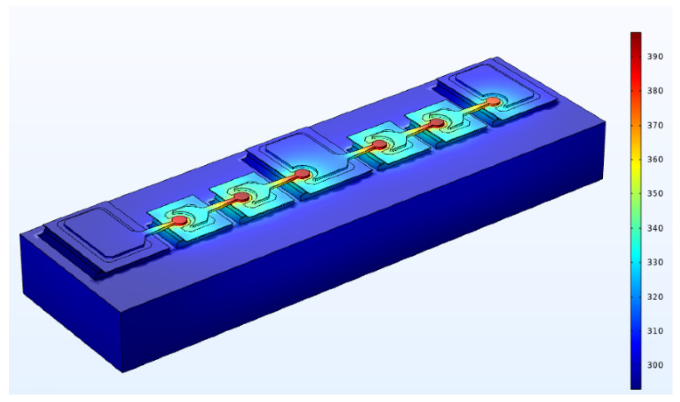
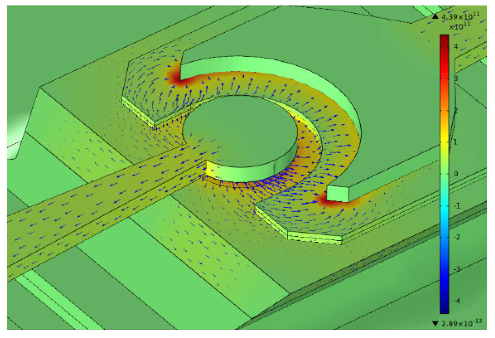
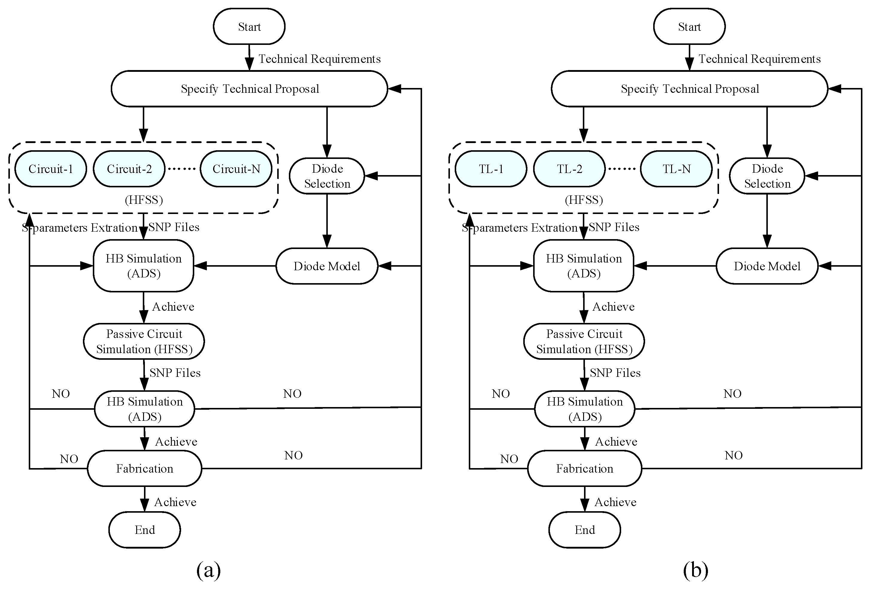
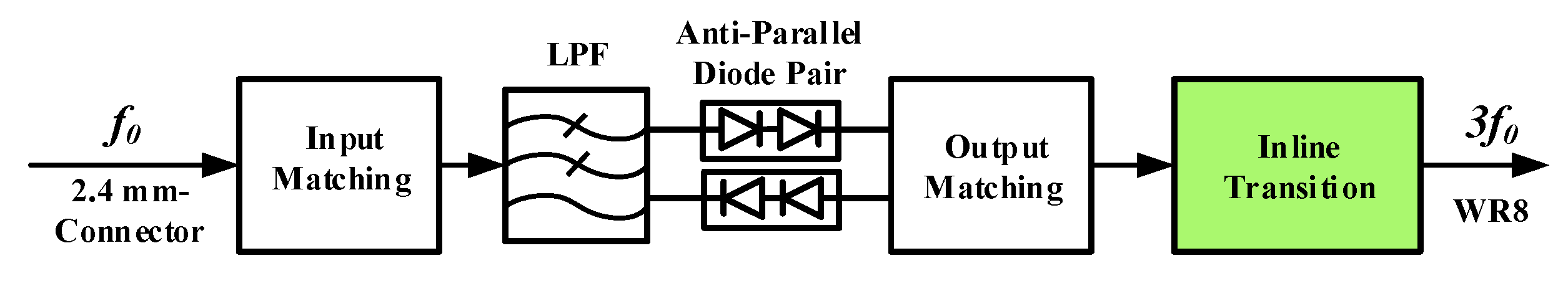
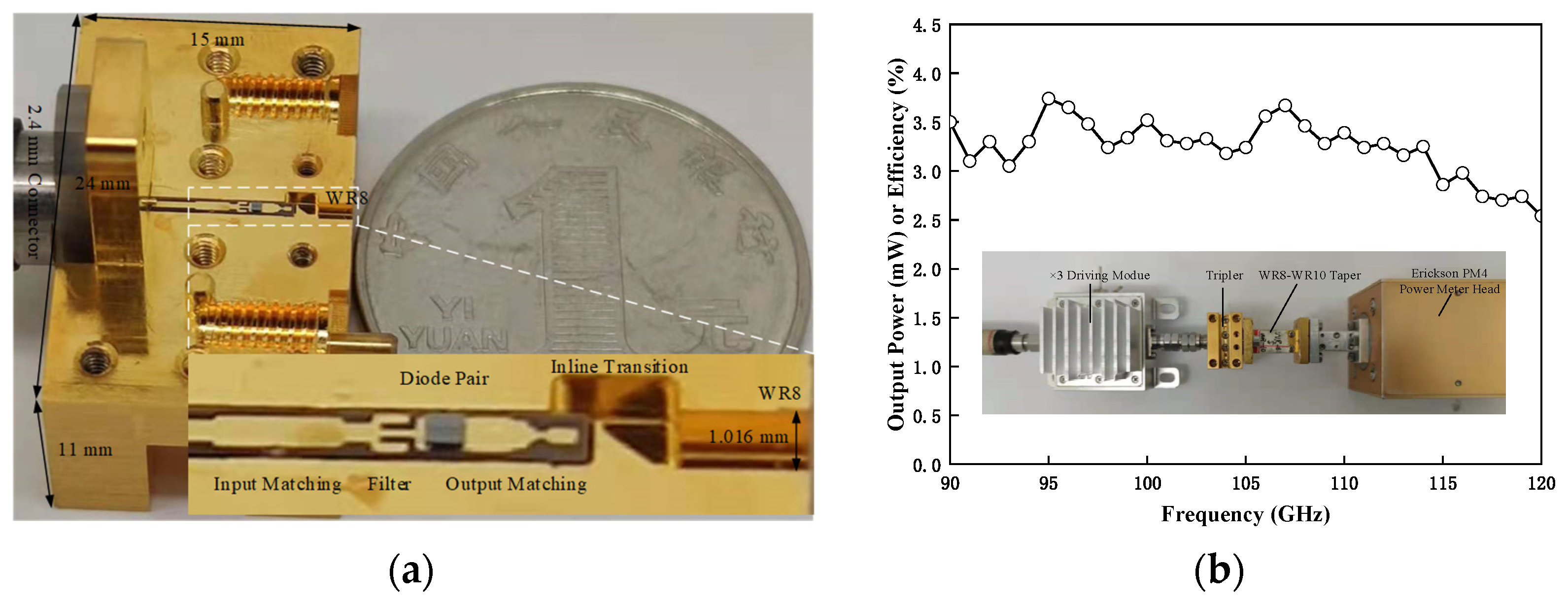
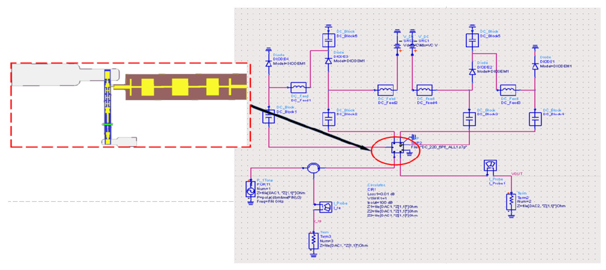
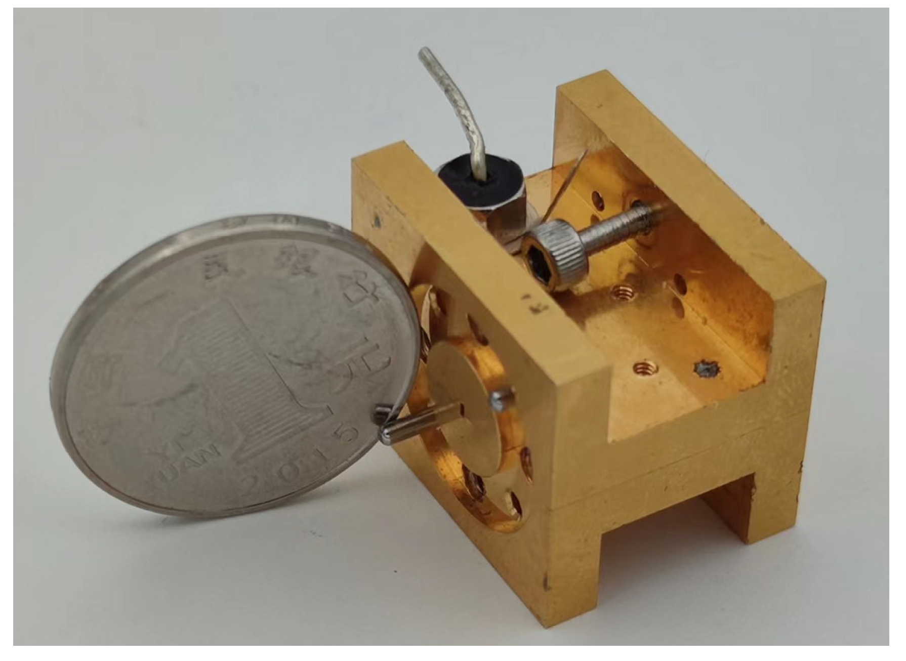
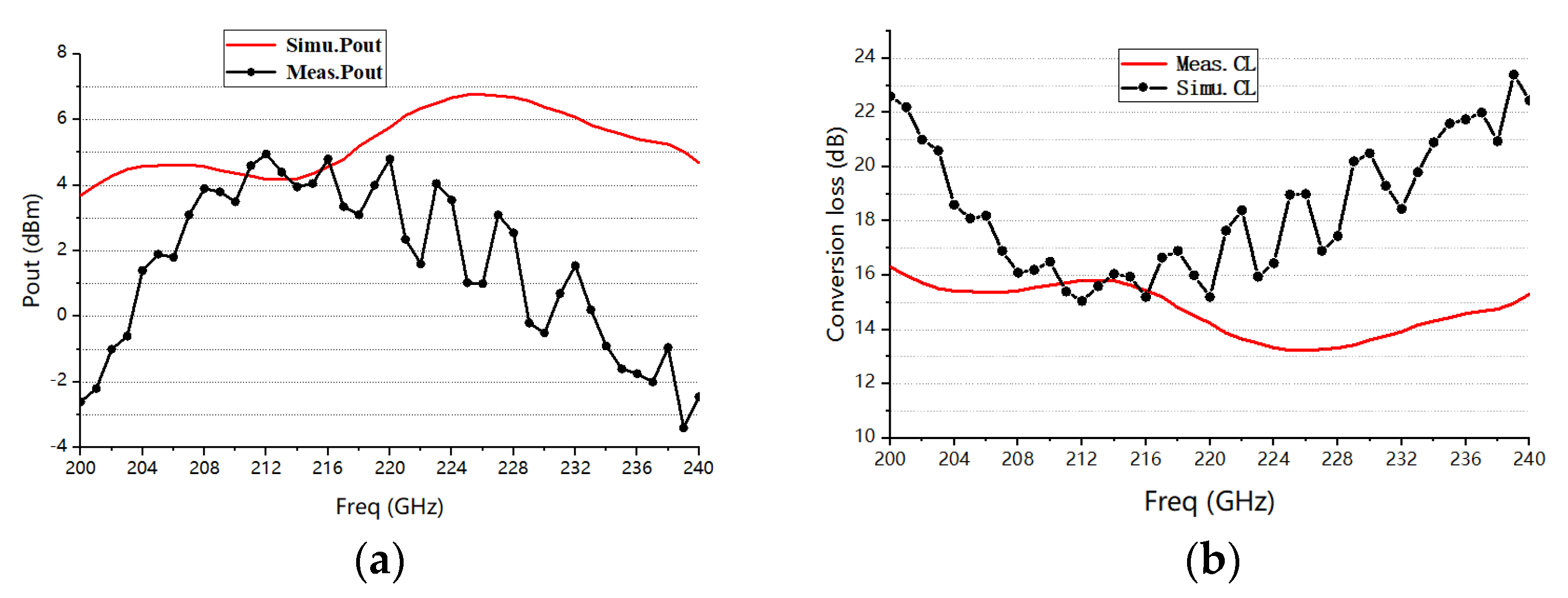
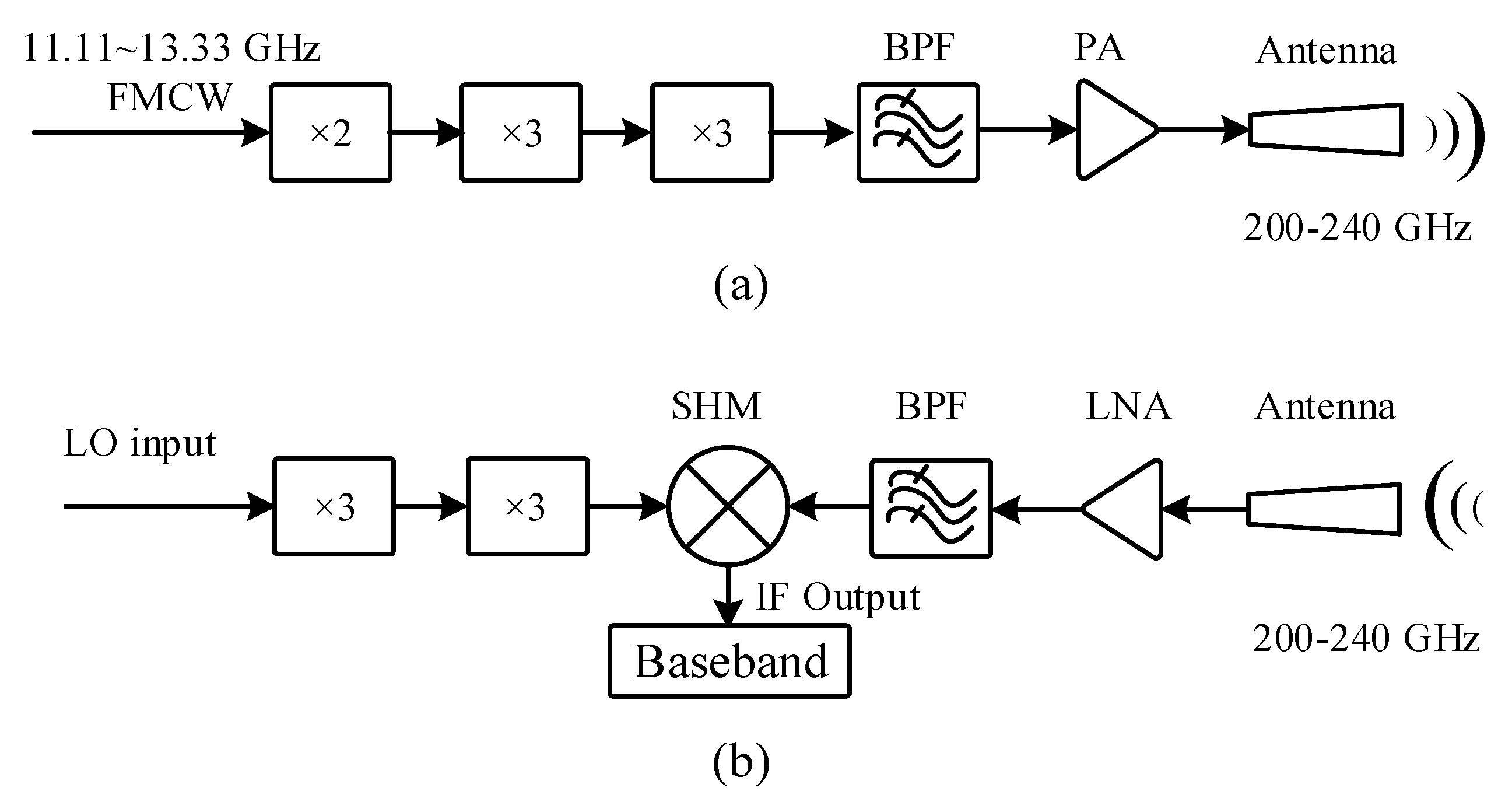
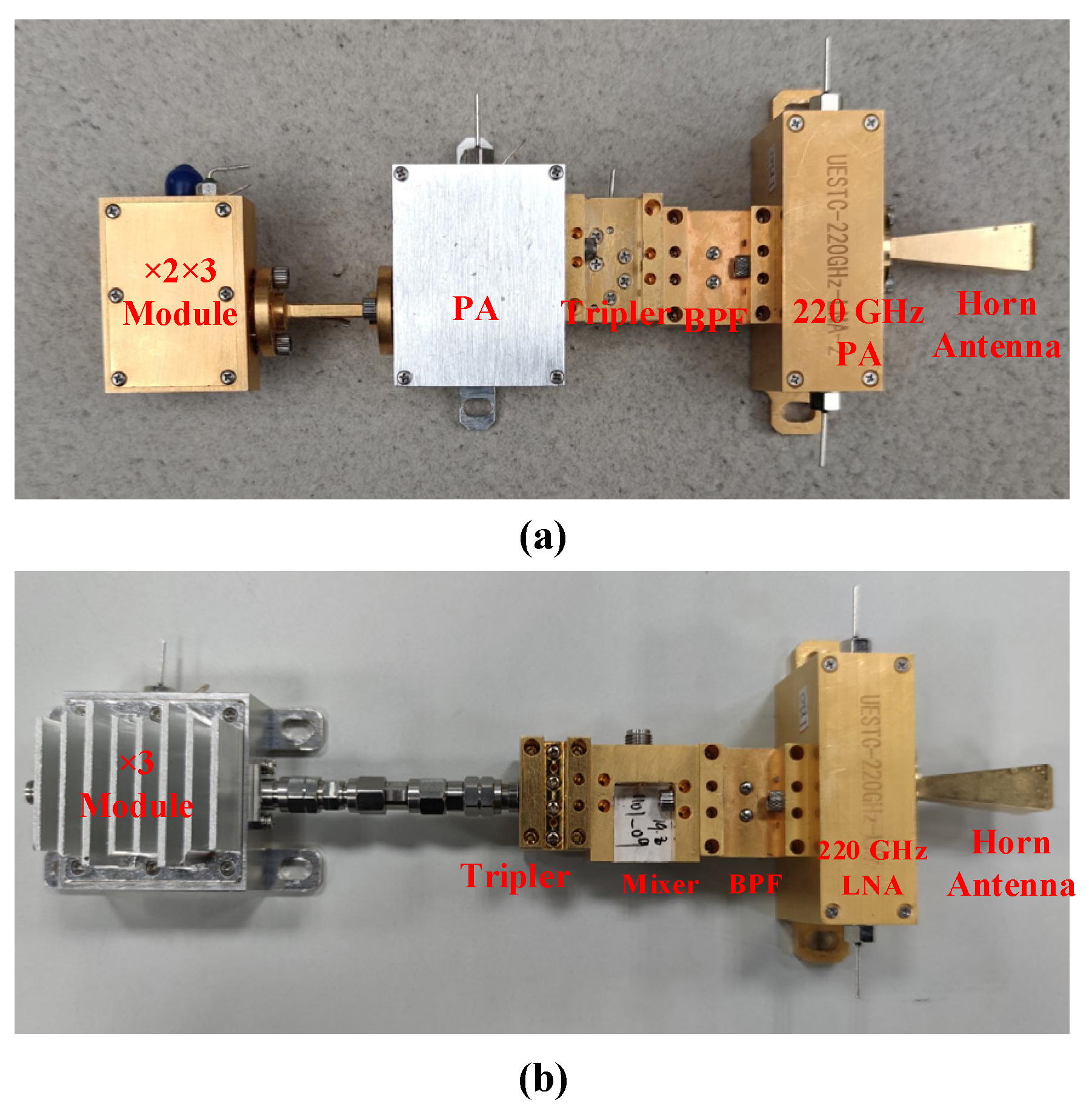
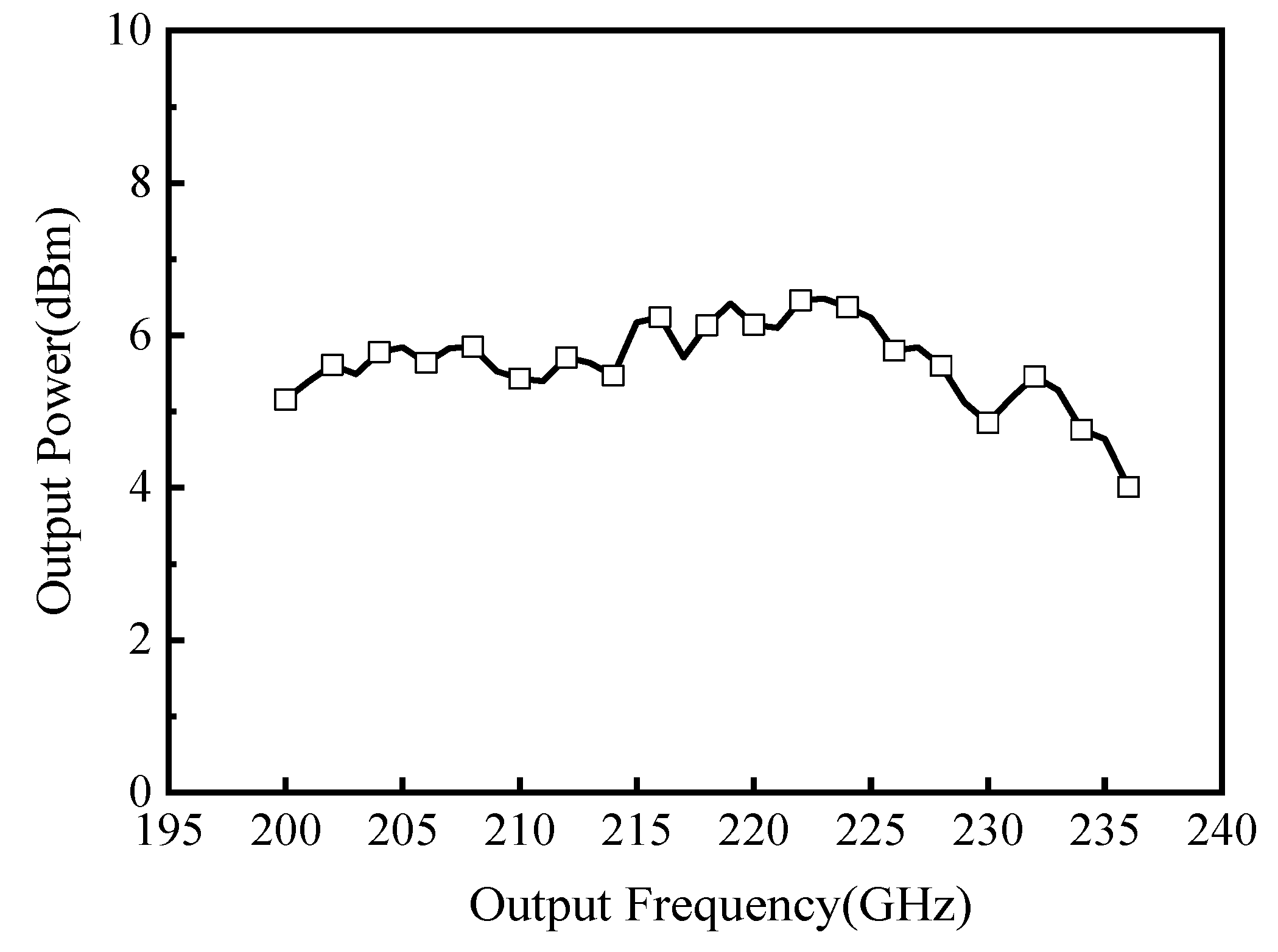
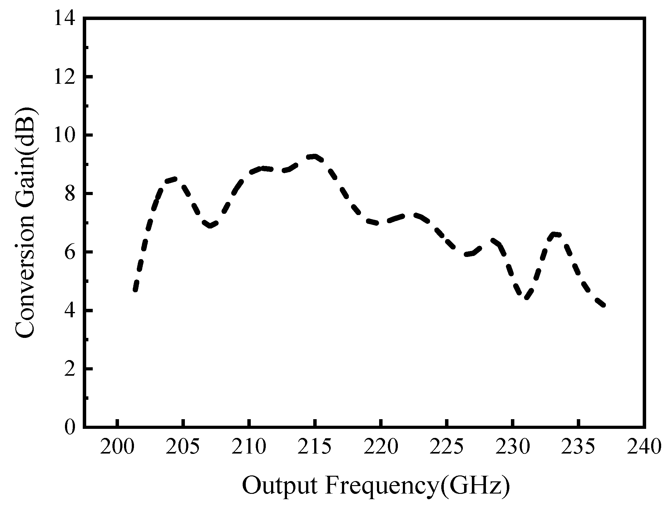
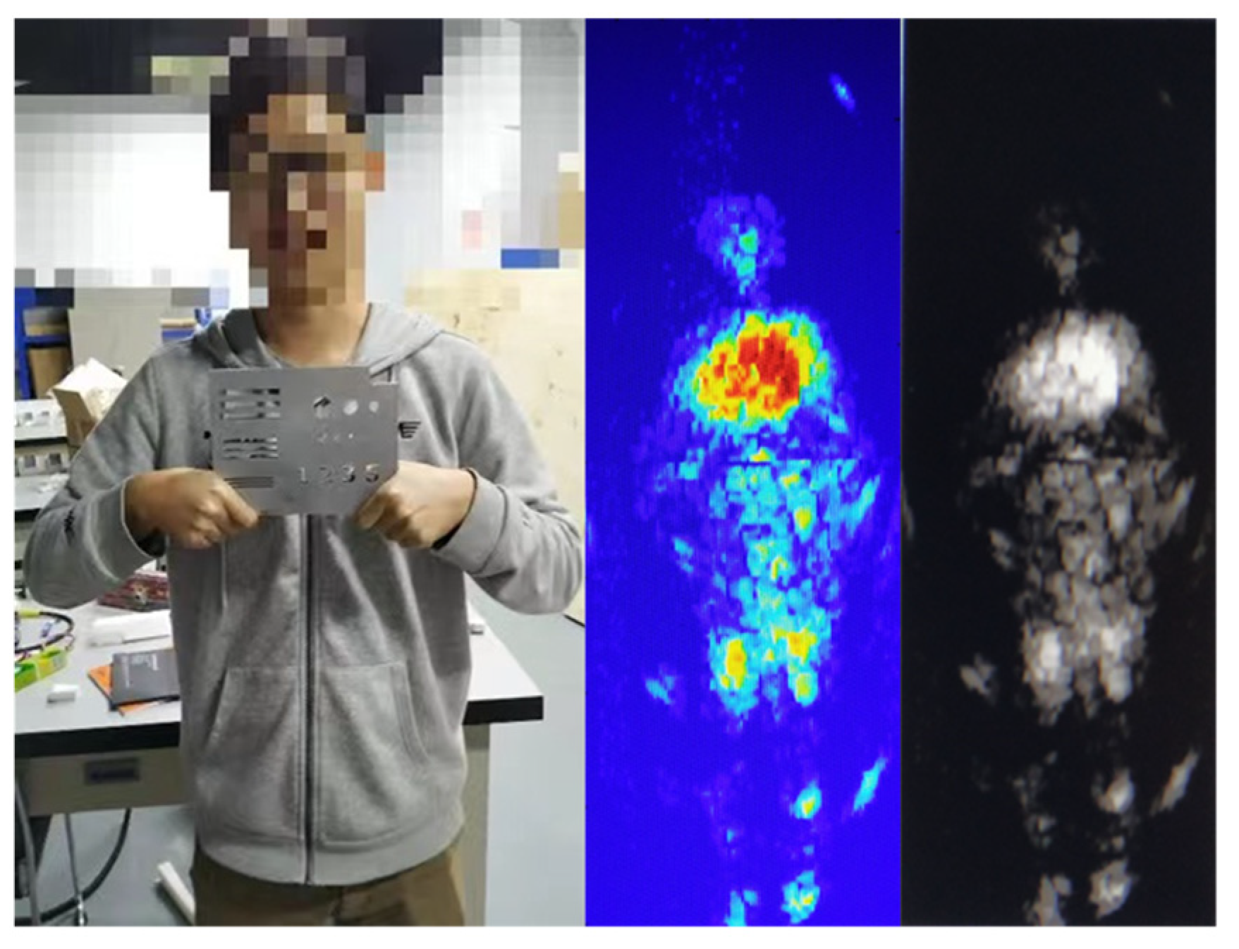
Table 1.
Performance summary and comparison between state-of-the-art frequency multipliers.
| Ref. | Freq. (GHz) | Harmonic | Pin (mW) | Peak Pout (mW) | Effi. (%) | FBW (%) | Device |
|---|---|---|---|---|---|---|---|
| [25] | 113 | ×3 | 1300 | 200 | 15 | 1.5 | HBVs |
| [26] | 282 | ×3 | 50–500 | 31 | ~7 | ~8.8 | HBVs |
| [50] | 135–190 | ×2 | 30–174 | 17.8 | 4–8 | 33.8 | GaAs SBDs |
| [51] | 165–200 | ×2 | 150–250 | ~100 | 40 | 20 | GaAs SBDs |
| [59] | 510–560 | ×3 | 350–400 | 30 | 8–9 | 11.3 | GaAs SBDs |
| [65] | 305–340 | ×2 | 15–33 | 3.5 | ~13.6 | 10.9 | GaAs SBDs |
| [66] | 177–183 | ×2 | 2000 | 200–244 | 9.5–11.8 | 3.3 | GaN SBDs |
| [69] | 150–170 | ×2 | 100–150 | 35 | ~25 | 10 | GaAs SBDs |
| [70] | 135–150 | ×3 | 50–70 | 3 | 3.9–4.9 | 10.5 | GaAs SBDs |
Publisher’s Note: MDPI stays neutral with regard to jurisdictional claims in published maps and institutional affiliations. |
© 2022 by the authors. Licensee MDPI, Basel, Switzerland. This article is an open access article distributed under the terms and conditions of the Creative Commons Attribution (CC BY) license (https://creativecommons.org/licenses/by/4.0/).
Share and Cite
MDPI and ACS Style
Zhang, Y.; Wu, C.; Liu, X.; Wang, L.; Dai, C.; Cui, J.; Li, Y.; Kinar, N. The Development of Frequency Multipliers for Terahertz Remote Sensing System. Remote Sens. 2022, 14, 2486. https://0-doi-org.brum.beds.ac.uk/10.3390/rs14102486
AMA Style
Zhang Y, Wu C, Liu X, Wang L, Dai C, Cui J, Li Y, Kinar N. The Development of Frequency Multipliers for Terahertz Remote Sensing System. Remote Sensing. 2022; 14(10):2486. https://0-doi-org.brum.beds.ac.uk/10.3390/rs14102486
Chicago/Turabian StyleZhang, Yong, Chengkai Wu, Xiaoyu Liu, Li Wang, Chunyue Dai, Jianhang Cui, Yukun Li, and Nicholas Kinar. 2022. "The Development of Frequency Multipliers for Terahertz Remote Sensing System" Remote Sensing 14, no. 10: 2486. https://0-doi-org.brum.beds.ac.uk/10.3390/rs14102486
Note that from the first issue of 2016, this journal uses article numbers instead of page numbers. See further details here.