Sidewall Slope Control of InP Via Holes for 3D Integration


1
Division of System IC Development, National Nanofab Center, Daejeon 34141, Korea
2
Division of Nano Patterning Process, National Nanofab Center, Daejeon 34141, Korea
3
Division of Nano Thin Film Process, National Nanofab Center, Daejeon 34141, Korea
*
Authors to whom correspondence should be addressed.
Micromachines 2021, 12(1), 89; https://0-doi-org.brum.beds.ac.uk/10.3390/mi12010089
Submission received: 1 December 2020
/
Revised: 11 January 2021
/
Accepted: 14 January 2021
/
Published: 16 January 2021
Abstract
:This is the first demonstration of sidewall slope control of InP via holes with an etch depth of more than 10 μm for 3D integration. The process for the InP via holes utilizes a common SiO2 layer as an InP etch mask and conventional inductively coupled plasma (ICP) etcher operated at room temperature and simple gas mixtures of Cl2/Ar for InP dry etch. Sidewall slope of InP via holes is controlled within the range of 80 to 90 degrees by changing the ICP power in the ICP etcher and adopting a dry-etched SiO2 layer with a sidewall slope of 70 degrees. Furthermore, the sidewall slope control of the InP via holes in a wide range of 36 to 69 degrees is possible by changing the RF power in the etcher and introducing a wet-etched SiO2 layer with a small sidewall slope of 2 degrees; this wide slope control is due to the change of InP-to-SiO2 selectivity with RF power.
1. Introduction
Owing to the excellent electron mobility characteristic of InAs, InGaAs, and InAlAs materials monolithically grown on InP substrate, InP-based electrical semiconductor device technologies such as high electron mobility transistors (HEMT), heterojunction bipolar transistors (HBT), and resonant tunneling diodes (RTD) have been demonstrated with maximum oscillation frequencies exceeding one terahertz [1,2,3]. To optimally exploit these high-frequency InP devices in system applications for millimeter-imaging and wideband communication, InP technologies have been integrated with Si or GaN technologies, which play a role of peripheral ICs or high-power ICs, respectively. Of various integration technologies, three-dimensional (3D) integration technologies have recently been demonstrated; compared to two-dimensional (2D) technologies, these 3D technologies minimize the resistance of interconnect-lines and improve chip density [4,5,6].
InP-based 3D integration technology has a core process called through-substrate-via (TSV), which forms via holes in the InP substrate and fills them with low-resistivity metals [6]. Similar to the Si TSV process, the InP TSV process has been realized by performing metal deposition on InP via holes followed by chemical-mechanical-polishing (CMP) [6]. However, the InP CMP process has to be handled carefully due to the fragile nature of InP substrates and equipment for InP CMP is uncommon and difficult for researchers to access. Instead of the CMP-based TSV process, an electro-plating (EP)-based TSV process, which performs seed metal deposition on InP via holes followed by EP, can be utilized. While the CMP-based TSV process completely fills via holes with metals, the EP-based process deposits thin metals with a thickness of only a few micrometers (μm) on the edges of the InP via holes. Because a few-μm-thick edge-deposited metal layers based on Cu or Au do not degrade the interconnect resistance of InP TSV because the skin depth, given by 1/(πfμσ)2 [7], where f is the operating frequency, μ is the relative permeability and σ is the conductivity, of low resistivity metals such as Cu or Au is calculated to be less than 0.5 micrometer (μm) in millimeter-wave frequency range of more than 30 GHz, the EP-based TSV process has recently been utilized as a useful hole filling method for InP TSV [8].
Because sputter equipment has better step coverage than that of evaporator equipment, seed metals in the EP-based InP TSV process have mainly been deposited mainly by sputtering. However, sputter-based seed metal deposition is known to suffer from shadowing effects when the aspect ratio (AR) of via holes, defined as the ratio of the height to the width of the structures, is more than one, leading to poor step coverage on via hole sidewalls [9]. As shown in our experimental results in Figure 1, it was revealed that Ti/Cu EP and seed metals on a sidewall of InP via holes with vertical slope of 90 degrees were not deposited. Accordingly, process methodology for controlling the sidewall slope of InP via holes should be presented so that they InP via holes have gradual sidewall slope. To date, most reports have focused only on implementing InP structures with vertical sidewall slopes approaching 90 degrees [10,11,12,13,14,15,16].
In this paper, we propose for the first time a process methodology for sidewall slope control of InP via holes. The etch depth of InP via holes is targeted to exceed 10 μm, because the depth of TSV for 3D integration has been decreased to about 10 μm, which corresponds to the limit value of the CMP processes [6,7]. The process for InP via holes with an etch depth of more than 10 μm utilizes a common SiO2 layer as an InP etch mask and conventional inductively coupled plasma (ICP) etcher and simple gas mixtures of Cl2/Ar for InP dry etch. By controlling input parameters for the ICP etcher, such as ICP power, RF power and gas mixture ratio, and changing the sidewall slope of the SiO2 layer, the sidewall slope of InP via holes is possible to adjust in a wide range of 36 to 90 degrees, while retaining high InP etch rate of 1 μm/min.
2. Materials and Methods
Figure 2 shows a cross-sectional view of a process flow for InP via holes. An InP substrate with S-doped, n-type and 100 orientation was used, provided by JX Nippon Mining & Metal Corporation. As shown in Figure 2a, a 1 μm thick SiO2 layer on the InP substrate was deposited by plasma-enhanced chemical vapor deposition (PECVD) at a temperature of 300 °C to use as an etch mask for InP dry etching. As shown in Figure 2b, a photoresist (PR) mask was formed by photolithography process with conditions of spinning rate of 3000 RPM, soft bake of 90 °C and 90 s, exposure time of 6 s, developing time of 50 s and hardbake of 150 °C and 15 min. The SiO2 layer was patterned by dry etching or wet etching process through the PR mask, as shown in Figure 2c. Dry etching process for the SiO2 layer was performed using an ICP etcher (Oxford Instruments Plasma Technology Plasmalab System 100) with conditions of CHF3/Ar of 20/10 sccm, ICP/RF power of 1500/300 W, operating pressure of 10 mTorr and operating time of total 15 min (5 times at 3 min a time). Wet etching process for the SiO2 layer was carried out by dipping the sample for 2.5 min in diluted HF (DHF) solution of HF:H2O = 1:3 with an SiO2 etch rate of 450 nm/min. The PR mask on the patterned SiO2 layer was removed using a DPSS-2200 solution, as shown in Figure 2d. The sidewall slope of the dry-etched or wet-etched SiO2 layers was defined as θ1, as can be seen in Figure 2d. Native oxide layer on the InP substrate was eliminated using a diluted HCl solution of HCl:DI = 1:10. The InP dry etching process was performed by using the ICP etcher, as shown in Figure 2e, and the SiO2 layer was removed by the DHF solution, as shown in Figure 2f. The sidewall slope of InP via holes was defined as θ2, as can be seen in Figure 2f.
The operation pressure, the temperature, and the type of the gas mixture are important input parameters of the ICP etcher for the InP dry etching process that determine the etch morphology of the InP via holes. Because the plasma environment in the etcher did not stably form at operating pressures of less than 4 mT, and because InP etch rate of InP via holes decreased considerably at operating pressures of more than 7 mT, the operating pressure in the ICP etcher for the InP dry etching was fixed at 5 mT. Because high operation temperature is known not to be necessary to achieve high InP etch rate of InP via holes when the reactive species densities are high [11,14], the operation temperature of the etcher for InP dry etching was set at room temperature while maintaining ICP power higher than 1000 W. CH4-based gas mixtures demonstrated slow InP etch rate and polymer deposition issues [11], and so chlorine (Cl2)-based gas mixtures of Cl2/Ar were used in this work to achieve high InP etch rate of InP via holes.
Each fabrication run consisted of 14 samples with a size of 2 cm × 2 cm. Twenty InP via holes with the same layout width of 10 μm were arranged in each sample. Different InP etching conditions were applied to each sample, by varying the RF power, gas mixture ratio, and ICP power of the ICP etcher for the InP dry etching process. A total of three fabrication runs were carried out to identify parameter deviation caused by process variation. The etching morphology of the fabricated InP via holes was observed using scanning electron microscope (SEM) equipment of S-4800 (Hitachi, Ltd., Tokyo, Japan).
3. Results and Discussion
3.1. InP via Holes with Steep Sidewall Slopes of 80 to 90 Degrees
To implement InP via holes with steep sidewall slope of more than 80 degrees, a dry-etched SiO2 layer with an average θ1 of 70 degrees as an etch mask for InP dry etching was utilized, as shown in Figure 3.
An experiment to determine the appropriate value of RF power in the ICP etcher for InP dry etching was performed. The fabrication results of InP via holes etched at different levels of RF power of 275 W, 288 W, 294 W, and 300 W are shown in Figure 4, where Figure 4a,b show SEM images of representative etch profiles and the InP etch rate and sidewall surface roughness of the fabricated InP via holes, respectively. Error bars in Figure 4b represent the deviation values incurred by the process variation for a total of 60 InP via holes with the same layout width in the three fabrication lots. ICP power and Cl2/Ar gas mixture of the ICP etcher were fixed at 1200 W and 20/15 sccm, respectively. An InP via hole with an RF power of 300 W showed a bad sidewall profile, as can be seen in Figure 4a, exhibiting a high average sidewall surface roughness of 1.65 μm, as shown in Figure 4b. This bad profile phenomenon is attributed to the strong Ar-ion bombardment near the top of the InP via hole by the high electric field. As RF power decreased, InP etch rate showed a decreasing tendency and, especially, average InP etch rate at RF power of 275 W decreased to 0.9 μm/min, as shown in Figure 4b. From our experimental results, performing InP dry etching at once rather than carrying out it by dividing several times led to much less polymer deposition on the surfaces of InP via holes. When InP dry etching is performed at once, unintended abnormal behavior has occurred in case of processing time of the ICP etcher exceeding 10 min; there was a problem of redeposition of various polymers on the surface of the chamber due to the rise in temperature in the chamber. Therefore, the processing time of the ICP etcher for the InP dry etching must be limited to within 10 min; for this reason, to implement InP via holes with an etch depth of more than 10 μm in 10 min, the InP etch rate had to exceed 1 μm/min. Consquently, the correct value of RF power to form InP via holes with steep sidewall slope was in the range of about 280 W to 294 W. The sidewall roughness of InP via holes formed with the RF power values of 280–294 W was at most 310 nm. Because seed metals with thickness of more than 310 nm can be readily deposited using sputter equipment, the achieved roughness value of 310 nm does not have a significant effect on the performance of the EP-based InP TSV with metal thicknesses of a few-μm level. Regarding the roughness value of 310 nm, it was analyzed that 210 nm of this value is generated from the InP dry etching process because 100 nm of that value is the sidewall roughness of the dry-etched SiO2 layer itself, as can be seen in Figure 3.
The proper ratio for the gas mixture of Cl2/Ar was investigated. Figure 5 shows fabrication results for InP via holes etched at mixtures of 10Cl2/25Ar, 15Cl2/20Ar, 20Cl2/15Ar, and 30Cl2/5Ar, while fixing total gas flow rate at 35 sccm. Figure 5a,b show SEM images of representative etch profiles and the InP etch rate and bottom surface roughness of the fabricated InP via holes, respectively. Error bars in Figure 5b indicate the deviation values for a total of 60 InP via holes with the identical layout width in the three fabrication lots. ICP power and RF power of the ICP etcher were fixed at 1200 W and 294 W, respectively. Fabricated InP via holes with Ar-rich gas mixtures of 10Cl2/25Ar and 15Cl2/20Ar exhibited undercut profiles, as shown in Figure 5a, leading to seed metals not deposited on InP via hole, and rough bottom surface morphology, showing an average bottom surface roughness of 1.55 μm even at a slight Ar-rich mixture of 15Cl2/20Ar, as shown in Figure 5b. These bad morphologies are attributed to P deficiency phenomena in InP near the top of the sidewall and at the bottoms of InP via holes due to strong Ar-ion bombardment in the ICP etcher [17]. Compared to the Ar-rich mixtures-based InP via holes, Cl2-rich mixture-based InP via holes of 20Cl2/15Ar and 30Cl2/5Ar exhibited improved morphology without undercut shape or rough bottom surface issues, as shown in Figure 5a. The average bottom surface roughness of 0.65 μm for 30Cl2/5Ar is considered to result from the lack of physical desorption of chlorine-based etch products due to the lack of Ar-ion bombardment. As a result, gas mixture of 20Cl2/15Ar was selected to implement the InP via holes with steep sidewall slope, leading to InP via holes with bottom surface roughness of maximum 170 nm while maintaining an InP etch rate of more than 1 μm, as shown in Figure 5b.
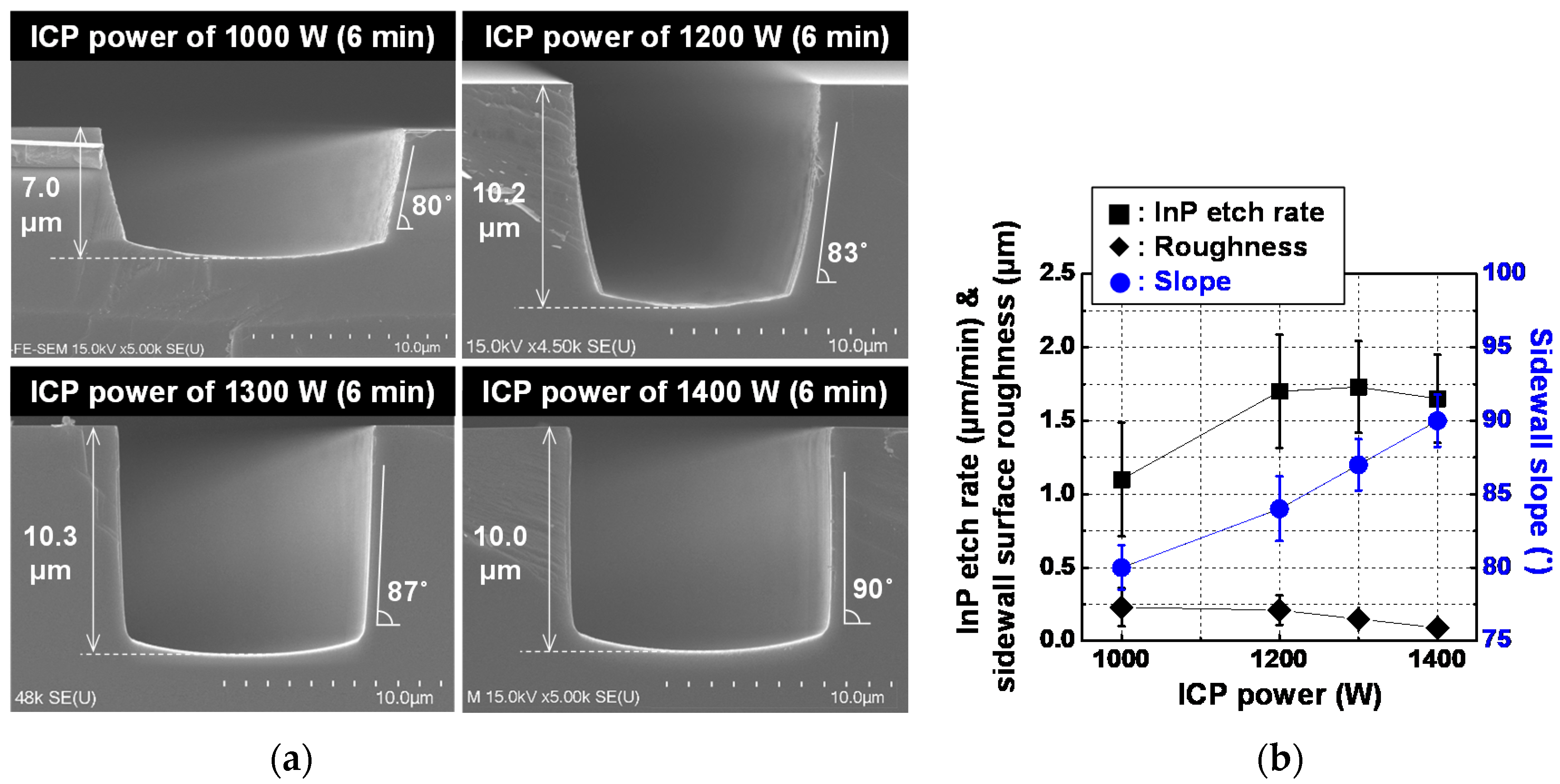
With selected conditions of RF power of 294 W and gas mixture of 20Cl2/15Ar, various sidewall slopes of InP via holes with steep sidewall slopes of more than 80 degrees were achieved by careful control of the ICP power. Fabrication results for InP via holes etched at different levels of ICP power is shown in Figure 6, where Figure 6a,b show SEM images of representative etch profiles and the InP etch rate, sidewall surface roughness and sidewall slope of the fabricated InP via holes, respectively. Error bars represent the deviation values for a total of 60 InP via holes with the identical layout width in the three fabrication lots. ICP power of more than 1000 W was required to obtain InP etch rate of more than 1 μm/min. Average θ2 values of InP via holes changed almost linearly to 80, 84, 87, and 90 degrees at ICP power values of 1000, 1200, 1300, and 1400 W, respectively. It is considered that this change of the sidewall slope with ICP power originated from the increase of ion-assisted desorption on the sidewall surface of InP via holes due to the increase of ICP power. As the ICP power increased from 1000 W to 1400 W, the average sidewall surface roughness of the InP via holes improved from 230 nm to 90 nm, while maintaining the average InP etch rate of more than 1 μm/min, as shown in Figure 6b. For reference, the selectivity between the InP substrate and the SiO2 layer (InP-to-SiO2 selectivity), defined as the InP etch rate divided by SiO2 etch rate, showed average values of 12.5, 15.2, 15, and 13.3 at ICP power values of 1000, 1200, 1300, and 1400 W, respectively.
3.2. InP via Holes with Gradual Sidewall Slopes of 36 to 69 Degrees
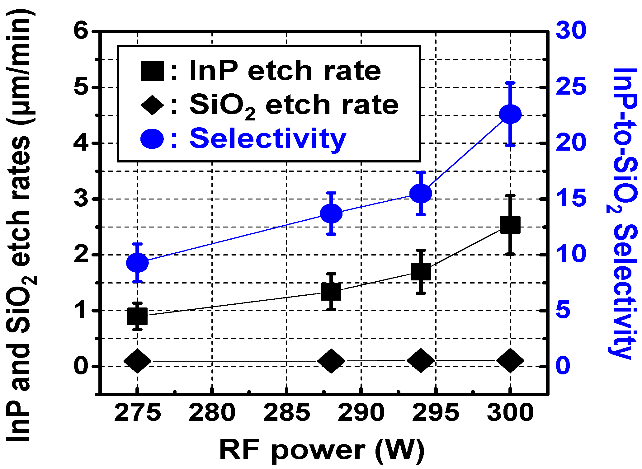
InP-to-SiO2 selectivity was analyzed by re-visiting the experimental results of InP via holes etched at different levels of RF power, mentioned in chapter 3.1. Figure 7 shows InP-to-SiO2 selectivity as a function of RF power. As RF power increased from 275 W to 300 W, average InP-to-SiO2 selectivity increased from 9.3 to 22.6. This increase in selectivity occurred because average InP etch rate increased from 0.9 to 2.54 μm/min, while the average SiO2 etch rate remained constant in a range of 0.10 to 0.11 μm/min. We utilized this characteristic of InP-to-SiO2 selectivity versus RF power for slope control of InP via holes with gradual sidewall slopes.
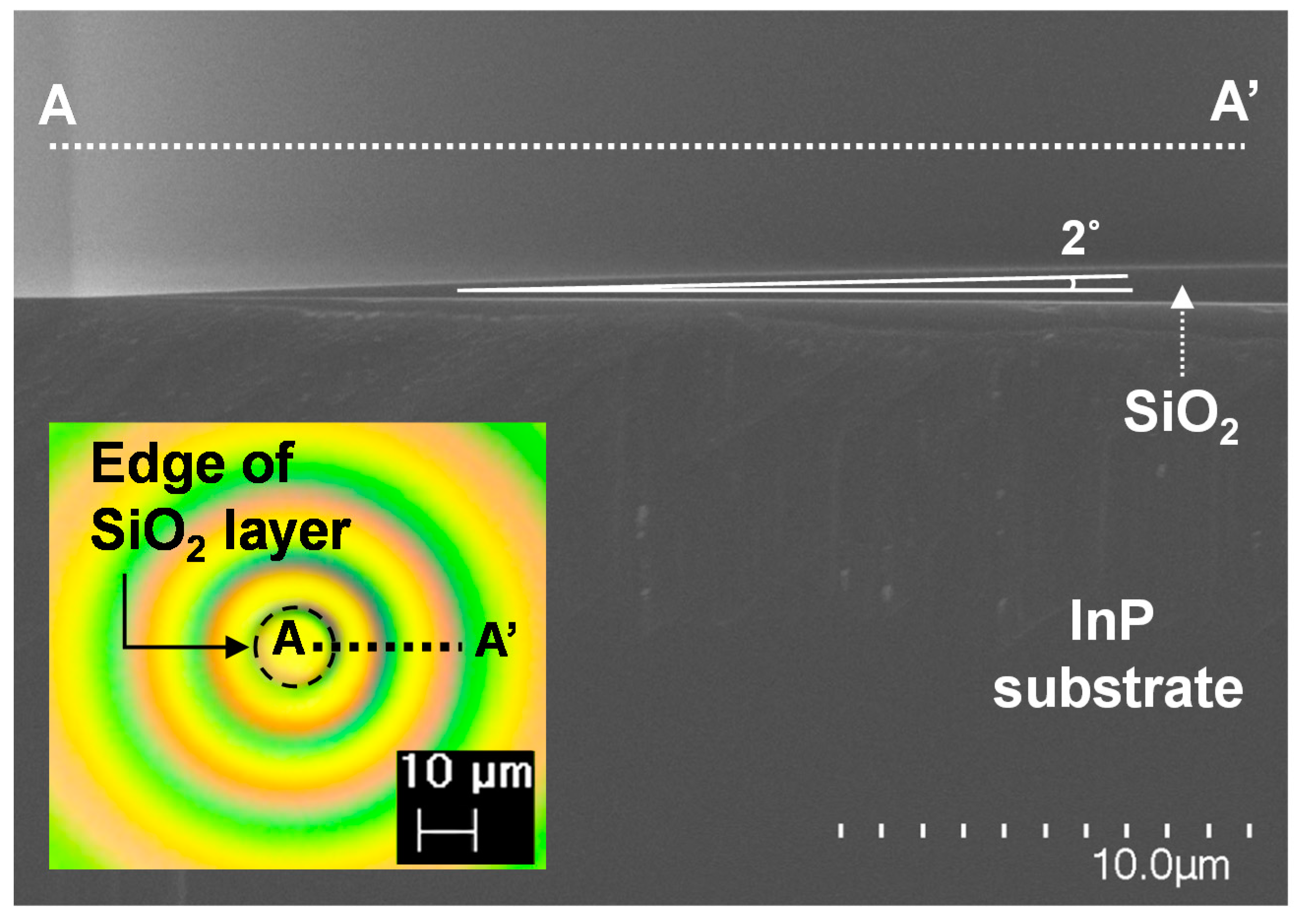
To realize InP via holes with gradual sidewall slopes, a SiO2 hard mask layer with fairly small θ1 values of only a few degrees was required. Table 1 shows specific process flow and measured results for the SiO2 layer with a small slope. Instead of dry etching, a wet-etching process was selected to implement the SiO2 layer with gradual sidewall slopes. To identify an appropriate etchant for SiO2 wet etching, a 20:1 buffered oxide etch (BOE) solution with a mixture ratio of NH4F:HF = 38.1:2.4% and a DHF solution with a mixture ratio of HF:H2O = 1:3 were tested. Under the same hard bake process conditions of 120 °C and 15 min, the SiO2 layers wet-etched using the DHF solution exhibited an average θ1 of 2.55 degrees, while the SiO2 layers wet-etched using the BOE solution showed an average θ1 of 44.25 degrees. Because the θ1 value of 44.25 degrees of the BOE-based SiO2 layers was too large to implement InP via holes with gradual sidewall slopes when considering the above-mentioned values of InP-to-SiO2 selectivity, the DHF solution was chosen as an appropriate etchant for SiO2 wet etching. This smaller sidewall slope characteristic of the SiO2 layers based on the DHF solution compared to the BOE solution stems from the strong lateral etching property of concentrated HF. In addition, the hard bake conditions of baking temperature and baking time in the photo-lithography for the DHF-based SiO2 layers were optimized. At hard bake conditions of 120 °C and 5 min, there was a PR adhesion problem, where PR peeled from the SiO2 layers during the wet-etching process. By increasing the baking temperature from 120 °C to 150 °C while keeping the baking time above 15 min, the SiO2 layer wet-etched using the DHF exhibited a reproducible sidewall slope characteristic, demonstrating an average θ1 value and θ1 deviation of 2 degrees and ±5%, respectively, without a PR adhesion problem, as shown in Figure 8. The thickness of about 1 μm of the SiO2 layer was well maintained within ±2.7% deviation by using a PECVD equipment (SLR-730, UNAXIS, OC Oerlikon, Pfäffikon, Switzerland) operated at 300 degrees.
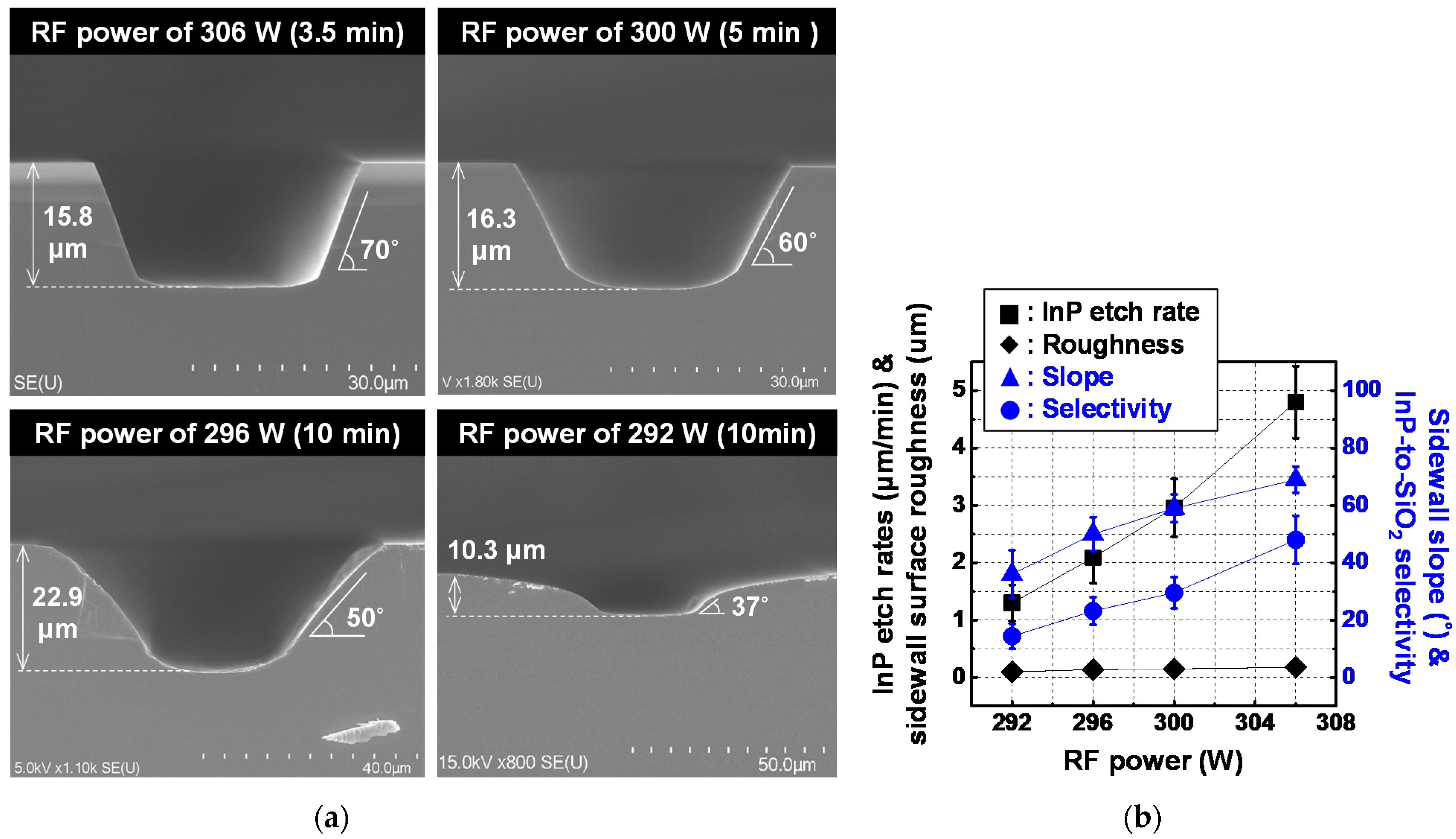
Figure 9 shows fabrication results for InP via holes etched at different levels of RF power using the wet-etched SiO2 layer, while fixing Cl2/Ar gas mixture and ICP power as 18/17 sccm and 1200 W, respectively. Figure 9a,b show SEM images of representative etch profiles and the InP etch rate, sidewall surface roughness, InP-to-SiO2 selectivity and sidewall slope of the fabricated InP via holes, respectively. Error bars represent the deviation values for 60 InP via holes with the identical layout width in the three lots. At values of RF power of 292, 296, 300, and 306 W, InP via holes exhibited average values of sidewall slope of 36, 50, 59, and 69 degrees, respectively, while maintaining InP etch rates of more than 1 μm/min. The two graphs of sidewall slope and InP-to-SiO2 selectivity as a function of RF power showed similar tendency, as shown in Figure 9b, which proves that this change of sidewall slope is attributed to the change of InP-to-SiO2 selectivity with RF power. For reference, surface roughness in the InP via holes with gradual sidewall slopes was at most 230 nm.
We should note that the proposed process method for obtaining gradual-sloped InP via holes leads to a penalty in area as an opportunity cost in providing the slope control technique. Table 2 shows a footprint comparison between the InP via holes with steep sidewall slopes and the InP via holes with gradual sidewall slopes. The footprint width (WFOOT) and footprint ratio (RFOOT) denote the average hole width of the top side of InP via holes and the WFOOT ratio of InP via holes with gradual sidewall slopes over InP via holes with steep sidewall slopes, respectively. The WFOOT value of the steep-sloped InP via holes was measured to be 11.5 μm and the WFOOT values of the gradual-sloped InP via holes with average θ2 values of 69, 59, 50, and 36 degrees were 36, 39.2, 62.4, and 101.3 μm, respectively, resulting in corresponding RFOOT values of 3.1, 3.4, 5.4, and 8.8. From our experimental results, it was verified that sputter-based seed metals were uniformly deposited on the sidewall of InP via holes with average θ2 values of less than 59 degrees, as shown in Figure 10, and thus the actual RFOOT value is regarded to be a maximum of 3.4.
4. Conclusions
Process methodology for sidewall slope control of InP via holes with an etch depth of more than 10 μm for 3D integration was proposed for the first time. The sidewall slope of InP via holes was controlled within the range of 80 to 90 degrees by changing the ICP power in the ICP etcher and utilizing a dry-etched SiO2 layer with a sidewall slope of 70 degrees. Furthermore, the sidewall slope of InP via holes was found to be widely adjustable within a range of 36 to 69 degrees, while maintaining high InP etch rate of 1 μm/min, by changing the RF power from 292 W to 306 W and using a wet-etched SiO2 layer with a small sidewall slope of 2 degrees; this wide slope control was due to the change of InP-to-SiO2 selectivity with RF power. This process methodology for InP via holes is expected to be widely used in implementing InP TSV for 3D integration because of utilization of a common SiO2 layer and conventional ICP etcher operated at room temperature and simple gas mixtures of Cl2/Ar for InP dry etch.
Author Contributions
Conceptualization, J.L. and Y.K.; Data curation, J.L. and K.R.; Formal analysis, J.L.; Investigation, J.L.; Methodology, J.L. and S.-K.L.; Resources, K.R.; Validation, J.L.; Writing — original draft, J.L.; Writing — review & editing, J.L., S.-K.L. and Y.K. All authors have read and agreed to the published version of the manuscript.
Funding
This research was supported by Civil-Military Technology Cooperation Program (No. 19-CM-BD-05).
Institutional Review Board Statement
Not applicable
Informed Consent Statement
Not applicable
Data Availability Statement
The data presented in this study are available in article here.
Acknowledgments
The authors thank Gi-Sung Lee of National Nanofab Center for technical discussions on the sidewall slope of the SiO2 layers.
Conflicts of Interest
The authors declare no conflict of interest.
References
- Mei, X.; Yoshida, W.; Lange, M.; Lee, J.; Zhou, J.; Liu, P.; Leong, K.; Zamora, A.; Padilla, J.; Sarkozy, S.; et al. First Demonstration of Amplification at 1 THz Using 25-nm InP High Electron Mobility Transistor Process. IEEE Electron. Device Lett. 2015, 36, 327–329. [Google Scholar] [CrossRef]
- Urteaga, M.; Griffith, J.; Young, J.; Pierson, R.; Rowell, P.; Seo, M.; Rodwell, M.J.W. A 130 nm InP HBT Integrated Circuit Technology for THz Electronics. In Proceedings of the IEEE IEDM, San Francisco, CA, USA, 3–7 December 2016; pp. 711–714. [Google Scholar] [CrossRef]
- Lee, J.; Kim, M.; Yang, K. A 1.52 THz RTD Triple-Push Oscillator with a μW-level Output Power. IEEE Trans. Terahertz Sci. Technol. 2016, 6, 336–340. [Google Scholar] [CrossRef]
- Kraemer, T.; Ostermay, I.; Jensen, T.; Johansen, T.K.; Schmueckle, F.-J.; Thies, A.; Krozer, V.; Heinrich, W.; Krueger, O.; Traenkle, G.; et al. InP-DHBT-on-BiCMOS Technology With f T / f max of 400/350 GHz for Heterogeneous Integrated Millimeter-Wave Sources. IEEE Trans. Electron. Devices 2013, 60, 2209–2216. [Google Scholar] [CrossRef]
- Urteaga, M.; Carter, A.; Griffith, Z.; Pierson, R.; Bergman, J.; Arias, A.; Rowell, P.; Hacker, J.; Brar, B.; Rodwell, M.J.W. THz Bandwidth InP HBT Technologies and Heterogeneous Integration with Si CMOS. In Proceedings of the 2016 IEEE Bipolar/BiCMOS Circuits and Technology Meeting (BCTM), New Brunswick, NJ, USA, 25–27 September 2016; pp. 35–41. [Google Scholar] [CrossRef]
- Carter, A.; Urteaga, M. 3D Integration Unites InP, GaN and Silicon CMOS. Compd. Semicond. 2018, 24, 50–53. Available online: https://compoundsemiconductor.net/article/104207/3D_Integration_Unites_InP_GaN_And_Silicon_CMOS (accessed on 9 November 2020).
- Wheeler, H.A. Formulas for the Skin Effect. Proc. IRE 1942, 30, 412–414. [Google Scholar] [CrossRef]
- Tsutsumi, T.; Hamada, H.; Sano, K.; Ida, M.; Matsuzaki, H. Feasibility Study of Wafer-Level Backside Process for InP-Based ICs. IEEE Trans. Electron. Devices 2019, 66, 3771–3776. [Google Scholar] [CrossRef]
- Karabacaka, T.; Lu, T.-M. Enhanced step coverage by oblique angle physical vapor deposition. J. Appl. Phys. 2005, 97, 124504. [Google Scholar] [CrossRef]
- Yoshikawa, T.; Kohmoto, S.; Ozaki, M.; Hamao, N.; Sugimoto, Y.; Sugimoto, M.; Asakawa, K. Smooth and vertical InP reactive ion beam etching with Cl2 ECR plasma. Jpn. J. Appl. Phys. 1992, 31, L655–L657. [Google Scholar] [CrossRef]
- Ko, K.K.; Pang, S.W. High Aspect Ratio Deep Via Holes in InP Etched Using CI2/Ar Plasma. J. Electrochem. Soc. 1995, 142, 3945–3949. [Google Scholar] [CrossRef]
- Deng, L.; Goodyear, A.L.; Dineen, M. ICP etching of InP and related materials using photoresist as mask. Proc. SPIE 2004, 5280, 838–843. [Google Scholar] [CrossRef]
- Docter, B.; Geluk, E.J.; Karouta, F.; Smit, M.K. Deep etching of DBR gratings in InP using Cl2 based ICP processes. In Proceedings Symposium IEEE/LEOS Benelux Chapter; Eindhoven University of Technology: Eindhoven, The Netherlands, 2006; pp. 97–100. [Google Scholar]
- Bae, J.W.; Jeong, C.H.; Lim, J.T.; Lee, H.C.; Yeom, G.Y. Anisotropic Etching of InP and InGaAs by Using an Inductively Coupled Plasma in Cl2/N2 and Cl2/Ar Mixtures at Low Bias Power. J. Korean Phys. Soc. 2007, 50, 1130–1135. [Google Scholar] [CrossRef]
- Bouchoule, S.; Azouigui, S.; Guilet, S.; Patriarche, G.; Largeau, L.; Martinez, A.; Gratiet, L.L.; Lemaitre, A.; Lelarge, F. Anisotropic and Smooth Inductively Coupled Plasma Etching of III-V Laser Waveguides Using HBr- O2 Chemistry. J. Electrochem. Soc. 2008, 155, H778–H785. [Google Scholar] [CrossRef]
- Lim, E.L.; Teng, J.H.; Chong, L.F.; Sutanto, N.; Chua, S.J.; Yeoh, S. Inductively Coupled Plasma Etching of InP with HBr∕O2 Chemistry. J. Electrochem. Soc. 2008, 155, D47–D51. [Google Scholar] [CrossRef]
- Lee, J.W.; Hong, J.; Pearton, S.J. Etching of InP at ≥ 1 μm/min in Cl2/Ar plasma chemistries. Appl. Phys. Lett. 1996, 68, 847–849. [Google Scholar] [CrossRef]
Figure 1.
Scanning electron microscope (SEM) images of InP via holes with vertical sidewall slope where electro-plating and seed metals were deposited. Sputtering process for seed metal deposition was performed by using equipment of SRN-110 (SORONA, Anseong, Korea) with a substrate-rotation function.

Figure 2.
Cross-sectional view of a process flow for InP via holes: (a) SiO2 deposition on InP substrate; (b) formation of photoresist (PR) mask; (c) SiO2 patterning through the PR mask; (d) PR removal; (e) dry etching of the InP substrate; (f) SiO2 removal. θ1 and θ2 are defined as sidewall slopes of the SiO2 layer and InP substrate, respectively.

Figure 3.
SEM images near a sidewall of a dry-etched SiO2 layer patterned on InP substrate.

Figure 4.
Fabrication results of InP via holes etched at different levels of RF power: (a) SEM images of representative etch profiles and (b) InP etch rate and sidewall surface roughness of InP via holes. Error bars in Figure 4b represent the deviation values incurred by the process variation for a total of 60 InP via holes with the same layout width in the three fabrication lots. ICP power, Cl2/Ar gas mixture, operation pressure, and operation temperature of the ICP etcher were 1200 W, 20/15 sccm, 5 mT and room temperature, respectively.

Figure 5.
Fabrication results of InP via holes etched at Cl2/Ar gas mixtures with different ratio of 10/25, 15/20, 20/15, and 30/5 sccm: (a) SEM images of representative etch profiles and (b) InP etch rate and bottom surface roughness of fabricated InP via holes. Error bars in Figure 5b represent the deviation values for a total of 60 InP via holes with the identical layout pattern in the three fabrication lots. Total gas flow rate, ICP power, RF power, operation pressure, and operation temperature of the ICP etcher were 35 sccm, 1200 W, 294 W, 5 mT and room temperature, respectively.

Figure 6.
Fabrication results of InP via holes etched at different levels of ICP power: (a) SEM images of representative etch profiles and (b) InP etch rate, sidewall surface roughness, and sidewall slope of fabricated InP via holes. Error bars in Figure 6b represent the deviation values for a total of 60 InP via holes with the identical layout pattern in the three fabrication lots. RF power, Cl2/Ar gas mixture, operation pressure and operation temperature of the ICP etcher were 294 W, 20/15 sccm, 5 mT and room temperature, respectively.

Figure 7.
Selectivity between the InP substrate and the SiO2 layer (InP-to-SiO2 selectivity) of InP via holes etched at different levels of RF power. Error bars represent the deviation values for a total of 60 InP via holes with the identical layout pattern in the three fabrication lots.
Figure 7.
Selectivity between the InP substrate and the SiO2 layer (InP-to-SiO2 selectivity) of InP via holes etched at different levels of RF power. Error bars represent the deviation values for a total of 60 InP via holes with the identical layout pattern in the three fabrication lots.

Figure 8.
SEM image near a sidewall of a wet-etched SiO2 layer patterned on InP substrate. Inset indicates a floor plan image of the patterned wet-etched SiO2 layer by microscope. Dotted circle in the inset marks the edge of the patterned SiO2 layer.
Figure 8.
SEM image near a sidewall of a wet-etched SiO2 layer patterned on InP substrate. Inset indicates a floor plan image of the patterned wet-etched SiO2 layer by microscope. Dotted circle in the inset marks the edge of the patterned SiO2 layer.

Figure 9.
Fabrication results of InP via holes etched at different levels of RF power using a wet-etched SiO2 layer as an etch mask for InP dry etch: (a) SEM images of representative etch profiles and (b) InP etch rate, sidewall surface roughness, sidewall slope and InP-to-SiO2 selectivity of InP via holes. Error bars in Figure 9b represent the deviation value incurred by process variation for a total of 60 InP via holes with the identical layout pattern in the three fabrication lots. ICP power, Cl2/Ar gas mixture, operation pressure, and operation temperature of the ICP etcher were 1200 W, 18/17 sccm, 5 mT, and room temperature, respectively.

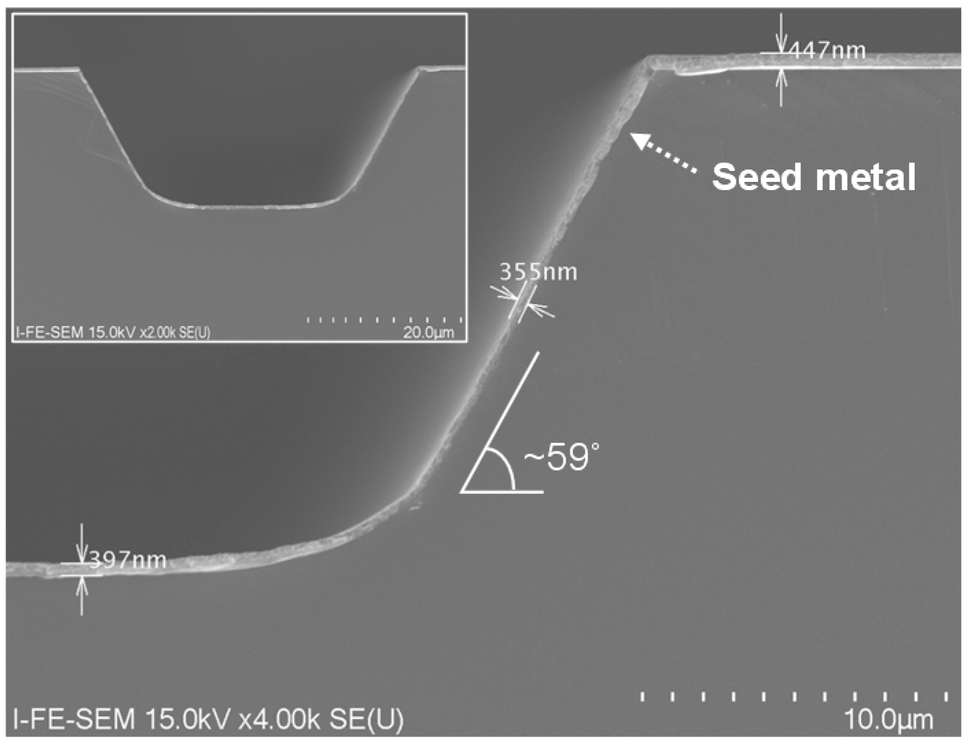
Figure 10.
SEM images of an InP via hole with a gradual sidewall slope of 59 degrees where seed metals were deposited.
Figure 10.
SEM images of an InP via hole with a gradual sidewall slope of 59 degrees where seed metals were deposited.


Table 1.
Specific process flow and measured results for the SiO2 layer with small sidewall slopes.
| Process Flow /Measurement | Description | Process Split #1 | Process Split #2 | Process Split #3 | Process Split #4 | Process Split #5 |
|---|---|---|---|---|---|---|
| Process flow for patterned SiO2 layer | SiO2 deposition | 300 °C in PECVD (UNAXIS SLR-730) | ||||
| Prebake | 120 °C, 10 min. | |||||
| HMDS | 3000 RPM for 30 s | |||||
| Photoresist (PR) | 3000 RPM for 30 s with i-1549 PR | |||||
| Soft bake | 90 °C, 90 s | |||||
| Exposure | 90 mJ | |||||
| Develop | 50 s in MIF 300 | |||||
| Hard bake | 120 °C, 5 min. | 120 °C, 15 min. | 120 °C, 15 min. | 150 °C, 15 min. | 150 °C, 30 min. | |
| PR Descum | O2 of 2500 sccm, pressure of 1 Torr, time of 20 s and room temp. in ICP PR Asher (DAS-2000, PSK, Hwaseong, Korea) | |||||
| Wet-etching | 2.5 min. in DHF 1 | 2.5 min. in DHF 1 | 23 min. in BOE 2 | 2.5 min. in DHF 1 | 2.5 min. in DHF 1 | |
| PR removal | Acetone—Isopropyl alcohol—DI | |||||
| Measurement of patterned SiO2 layer | Average thickness (μm) | - | 1.02 | 1.03 | 1.02 | 1.02 |
| Thickness deviation (%) | - | ±2.6 | ±2.7 | ±2.7 | ±2.6 | |
| Average sidewall slope (°) | - | 2.55 | 44.25 | 2 | 2 | |
| Sidewall slope deviation (%) | - | ±5.9 | ±2.8 | ±5 | ±5 | |
| Problem | PR adhesion | - | - | - | - | |
1 DHF: Dilute HF (hydrofluoric acid) solution with a mixture ratio of HF:H2O = 1:3; 2 BOE: Buffered oxide etch solution with a mixture ratio of NH4F:HF = 38.1 %:2.4 %.
Table 2.
Footprint comparison of fabricated InP via holes with various sidewall slopes.
| Type of Process | InP via Holes with Steep Sidewall Slopes | InP via Holes with Gradual Sidewall Slopes | |||
|---|---|---|---|---|---|
| Average θ2 1 (°) | 80–90 | 69 | 59 | 50 | 36 |
| WFOOT 2 (μm) | 11.5 | 36 | 39.2 | 62.4 | 101.3 |
| RFOOT 3 (μm/μm) | - | 3.1 | 3.4 | 5.4 | 8.8 |
1 θ2: The sidewall slope of InP via holes; 2 WFOOT: The average footprint width of InP via holes; 3 RFOOT: The WFOOT ratio of InP via holes with gradual sidewall slopes over InP via holes with steep sidewall slopes.
Publisher’s Note: MDPI stays neutral with regard to jurisdictional claims in published maps and institutional affiliations. |
© 2021 by the authors. Licensee MDPI, Basel, Switzerland. This article is an open access article distributed under the terms and conditions of the Creative Commons Attribution (CC BY) license (http://creativecommons.org/licenses/by/4.0/).
Share and Cite
MDPI and ACS Style
Lee, J.; Roh, K.; Lim, S.-K.; Kim, Y. Sidewall Slope Control of InP Via Holes for 3D Integration. Micromachines 2021, 12, 89. https://0-doi-org.brum.beds.ac.uk/10.3390/mi12010089
AMA Style
Lee J, Roh K, Lim S-K, Kim Y. Sidewall Slope Control of InP Via Holes for 3D Integration. Micromachines. 2021; 12(1):89. https://0-doi-org.brum.beds.ac.uk/10.3390/mi12010089
Chicago/Turabian StyleLee, Jongwon, Kilsun Roh, Sung-Kyu Lim, and Youngsu Kim. 2021. "Sidewall Slope Control of InP Via Holes for 3D Integration" Micromachines 12, no. 1: 89. https://0-doi-org.brum.beds.ac.uk/10.3390/mi12010089
Note that from the first issue of 2016, this journal uses article numbers instead of page numbers. See further details here.