
Electrical Characterizations of Planar Ga2O3 Schottky Barrier Diodes
by
 ,
,
Shiyu Zhang
1, 
Zeng Liu
1,2,3,
Yuanyuan Liu
4,5,
Yusong Zhi
1,
Peigang Li
1,*,
Zhenping Wu
1 and
Weihua Tang
1,2,3,* 1
Laboratory of Information Functional Materials and Devices, School of Science & State Key Laboratory of Information Photonics and Optical Communications, Beijing University of Posts and Telecommunications, Beijing 100876, China
2
College of Electronic and Optical Engineering & College of Microelectronics, Nanjing University of Posts and Telecommunications, Nanjing 210023, China
3
National and Local Joint Engineering Laboratory for RF Integration and Micro-Packing Technologies, Nanjing University of Posts and Telecommunications, Nanjing 210023, China
4
Center of Materials Science and Optoelectronics Engineering, University of Chinese Academy of Sciences, Beijing 100049, China
5
The Engineering Research Center for Semiconductor Integrated Technology, Institute of Semiconductors, Chinese Academy of Sciences, Beijing 100083, China
*
Authors to whom correspondence should be addressed.
Micromachines 2021, 12(3), 259; https://0-doi-org.brum.beds.ac.uk/10.3390/mi12030259
Submission received: 23 January 2021
/
Revised: 9 February 2021
/
Accepted: 1 March 2021
/
Published: 3 March 2021
(This article belongs to the Section A:Physics)
Abstract
:In this work, a Schottky barrier diode (SBD) is fabricated and demonstrated based on the edge-defined film-fed grown (EFG) Ga2O3 crystal substrate. At the current stage, for high resistance un-doped Ga2O3 films and/or bulk substrates, the carrier concentration (and other electrical parameters) is difficult to be obtained by using the conventional Hall measurement. Therefore, we extracted the electrical parameters such as on-state resistance (Ron), Schottky barrier height (), the ideal factor (n), series resistance (Rs) and the carrier concentration (Nd) by analyzing the current density–voltage (J–V) and capacitance–voltage (C–V) curves of the Ga2O3-based SBD, systematically. The detailed measurements and theoretical analysis are displayed in this paper.
1. Introduction
Owing to the suitable energy band gap (Eg) of ~4.9 eV, a high Baliga’s figure of merit (FOM) of more than 3200, a high Huang’s material FOM of 279, Johnson’s FOM of 2844, and a high theoretical breakdown field (EBR) of ~8 MV/cm, gallium oxide (Ga2O3) has been widely employed to construct optical detectors and power electronics along with low direct current losses and stable operations [1,2,3]. Till now, Ga2O3-based Schottky barrier diodes (SBDs) have achieved high breakdown voltages of 2300 V in a vertical edge-terminated SBD [4] and 3000 V in a lateral field-plated (FP) SBD [5], suggesting strong competitiveness superior to GaN and SiC. Owing to the low dark current and fast response speed [6], the Ga2O3-based Schottky diode photodetectors also have drawn much attention for high performances. For instance, the high photo responsivity (R), high external quantum efficiency (EQE), large specific detectivity (D*), and short response time in Ni/β-Ga2O3 [7], Pt/ε-Ga2O3 [8], graphene/β-Ga2O3 [9], and MXenes/β-Ga2O3 [10] photodiodes are realized.
In electronic devices, the electrical parameters, such as carrier concentration, are key issues that affect the device design, construction, and operation. For doped Ga2O3 and/or the flakes exfoliated from the bulk single crystal, the electron concentrations are reported as 1016–1020 cm−3 [11,12,13,14], while in fact, the un-doped Ga2O3 has a high resistance due to the large Eg, thus it is very hard to obtain some electrical parameters via the conventional Hall measurement. Additionally, a systematic and comprehensive study for electrical characterizations such as on-state resistance (Ron), Schottky barrier height (), the ideal factor (n), series resistance (Rs) and the carrier concentration (Nd) of Ga2O3 Schottky devices is less reported. Therefore, to solve this problem, we fabricated a Ga2O3-based SBD, and then performed the electrical characterizations through the J–V, H(J)–J, and C–V characteristic curves.
2. Experimental Section
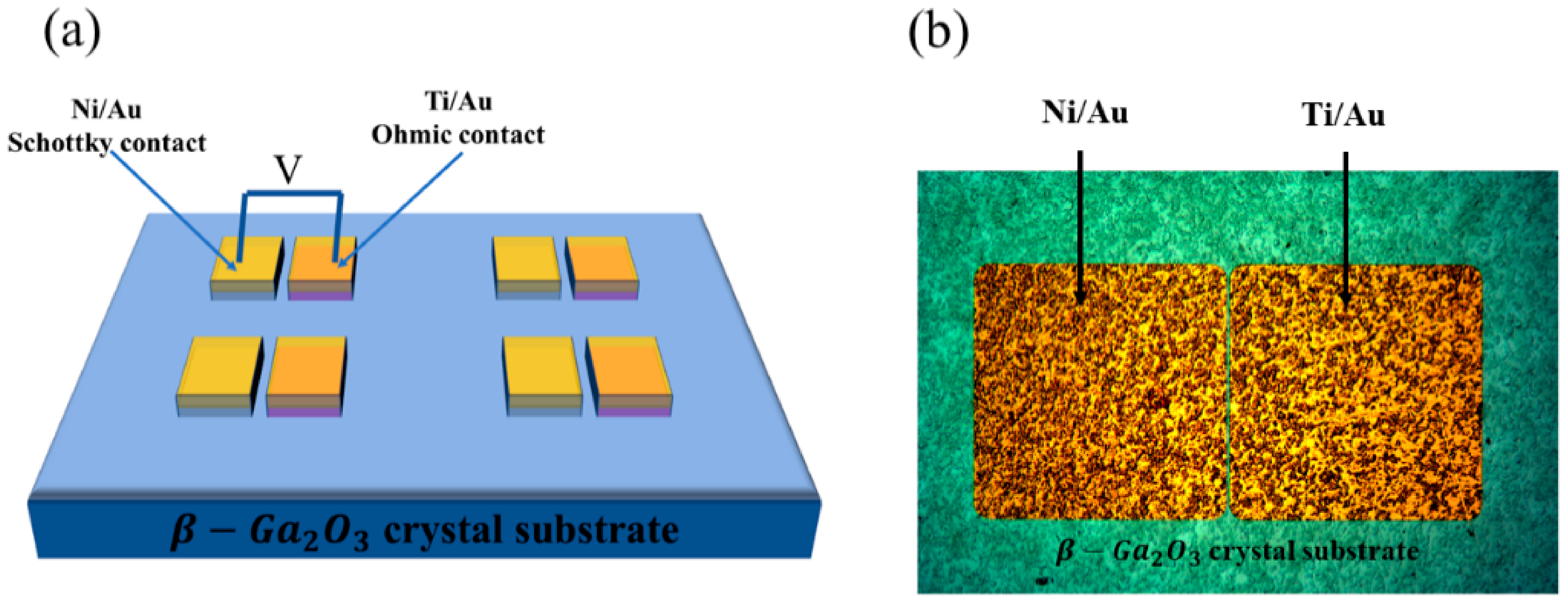
The Ga2O3 crystal substrate was grown by the edge-defined film-fed grown method, whose scale is 10 mm 10 mm. For fabricating the Schottky diode, photolithography, lift-off, and electron beam vapor techniques were used to finish the Ni/Au (Schottky, 30 nm/100 nm) and Ti/Au (Ohmic, 30 nm/100 nm) electrode patterns as shown in Figure 1b. X-ray diffraction (XRD), X-ray photoelectron spectroscopy (XPS), and scanning electron microscopy (SEM) were performed to verify the quality of the Ga2O3 crystal substrate. The electrical test was executed with Keithley 4200 analysis equipment in the air at room temperature. The area of the electrode pattern is 2.4 10−3 cm2. Figure 1a is the schematic of the planar Ga2O3 SBDs.
3. Results and Discussion
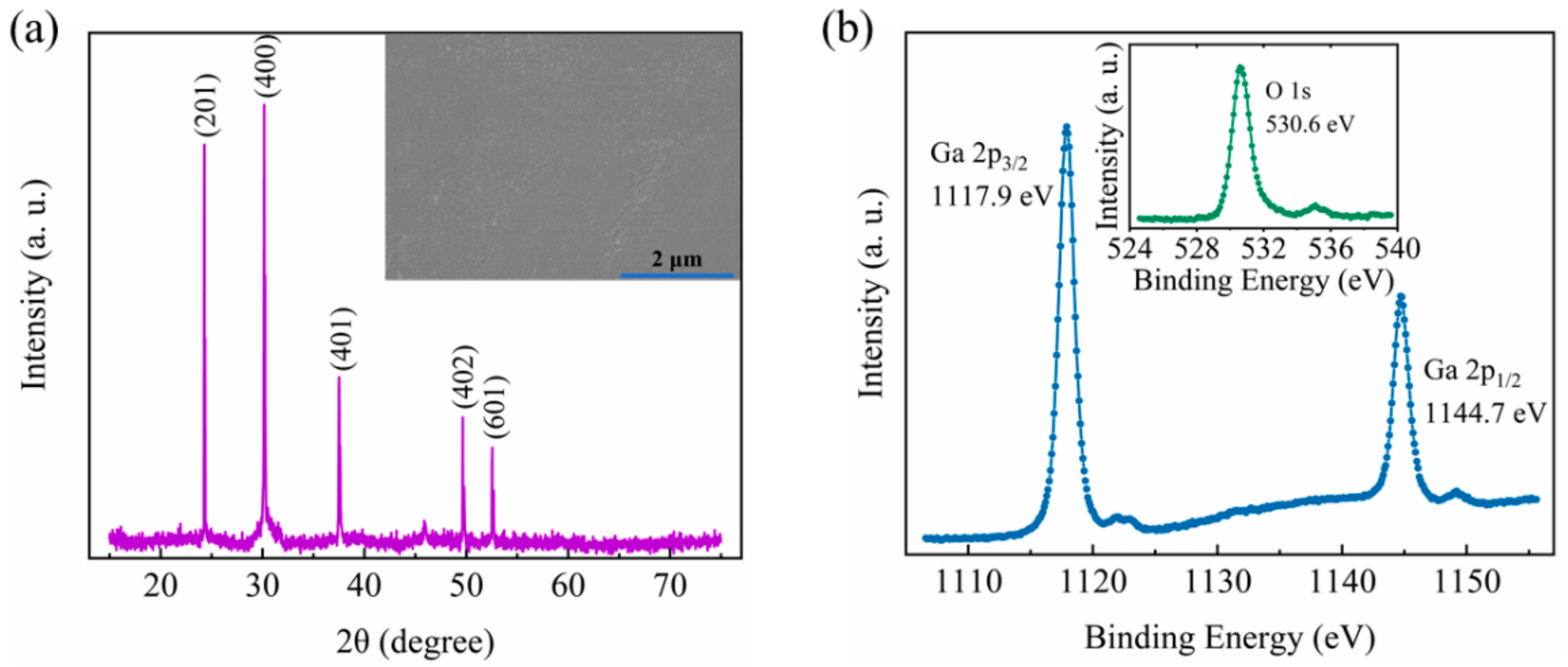
As shown in Figure 2a, the XRD pattern of the edge-defined film-fed (EFG)-grown Ga2O3 substrate is displayed, showing (201), (400), (401), (402), and (601) orientations. The prepared Ga2O3 crystal is polycrystalline β-Ga2O3. The SEM image of the surface of the Ga2O3 substrate is portrayed in Figure 2a inset, suggesting a decent crystallization with well-defined boundaries and uniform claviform grains. In Figure 2b, the binding energies of Ga 2p1/2, Ga 2p3/2, and O 1s are determined to be 1144.7 eV, 1117.9 eV, and 530.6 eV by XPS, they are similar to the reported values as shown in Table 1, verifying the formation of the Ga2O3 semiconductor.
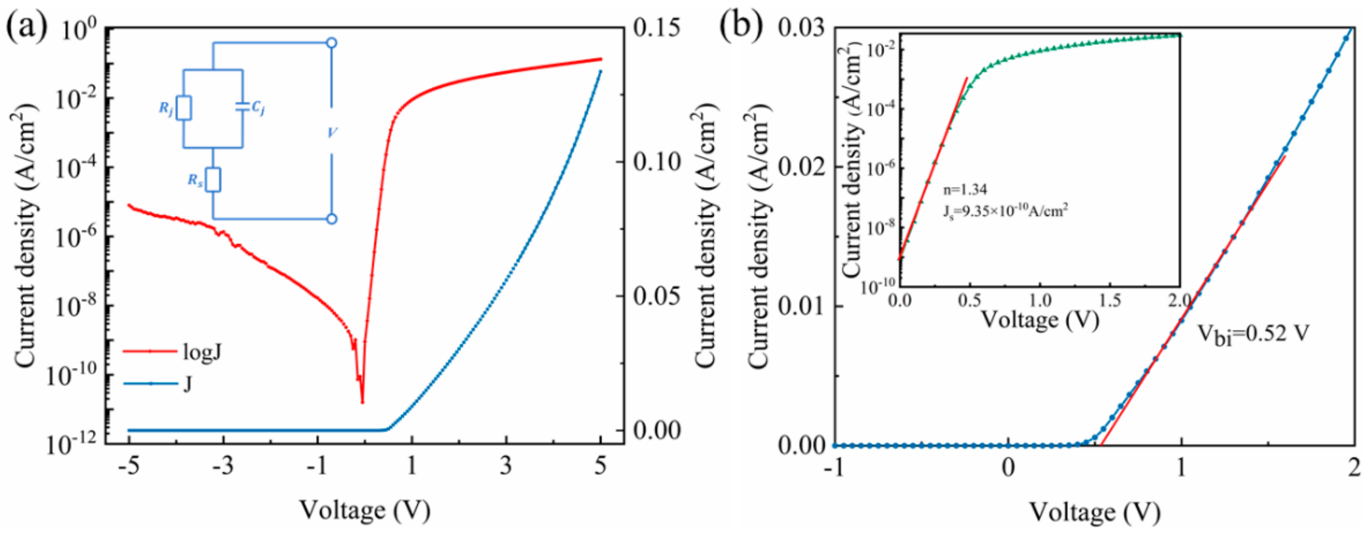
In Figure 3a, current density–voltage (J–V) curves of the Ni/Ga2O3/Ti Schottky diode are shown in linear-scale and semi-log scale, respectively. The output current density is 3.04 10−2 A/cm2 and 1.25 10−7 A/cm2 at 2 V and −2 V, respectively, translating to a high rectifying ratio of 2.44 105; the fabricated device is on-state at forward voltages while off-state at reverse voltages. By extrapolating the linear region of the log-scaled J–V curve in Figure 3a (red line) to obtain its slope, the on-state resistance (Ron) is estimated to be 51.5 Ω cm2. Furtherly, we use the thermionic emission (TE) model to describe the Ni/Ga2O3/Ti Schottky diode [18]:
and
where is the electron charge, V is the applied voltage, is the reverse saturation current, n is the ideal factor, k is the Boltzmann constant, T is the thermodynamic temperature, is the Schottky barrier height, and is the Richardson constant. For Ga2O3, its effective electron mass , with the mass of the free electron, thus the of Ga2O3 is calculated to be 41.07 A/cm2 K2 [19].
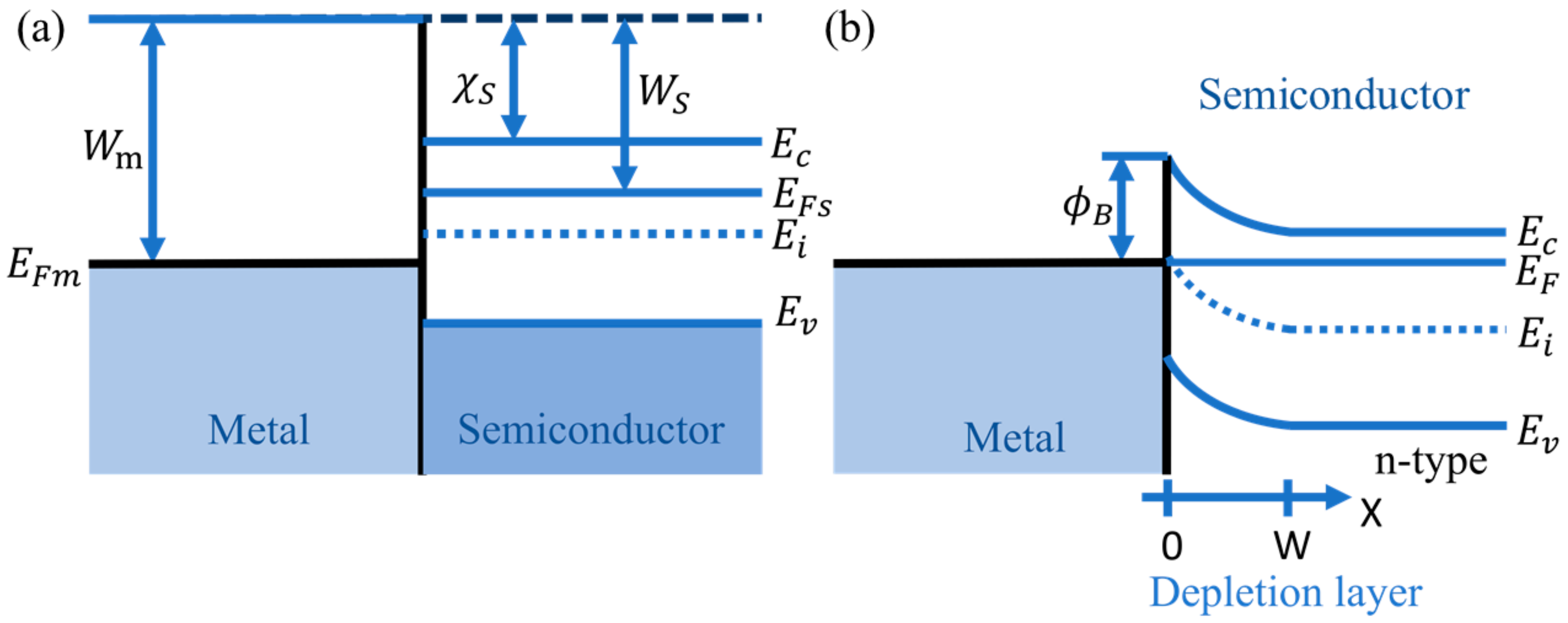
As displayed in Figure 3b, with the TE model described in Equations (1)–(4), the n, and turn-on voltage (Von) are determined to be 1.34, 0.93 eV, and 0.52 V, respectively. In Figure 3b inset, the of the Schottky diode is 9.35 10−10 A/cm2. The n value between 1 and 2, nearer to 1, indicates a decent Schottky electrical behavior in the fabricated device. The Von suggests a built-in potential difference (Vbi) of 0.52 eV. In fact, the work function of Ni (Wm) is 5.15 eV [20], and the electron affinity of Ga2O3 () is 4.00 eV [21]. The Ni-Ga2O3 energy band diagram before they make contact is shown in Figure 4a. According to the Schottky–Mott rule [22,23], the Ni-Ga2O3 interface barrier is about 1.15 eV, i.e., the difference between Wm and . After they make contact, as given Figure 4b, the conduction and valence energy band edge (Ec and Ev) bend up, owing to the electron transferring to the electrode. The formation of the indicates a barrier for electron transport in the device, thus the device has a Von and rectifying effect.
For the device, the series resistance (Rs) is a key parameter affecting the performances of the Schottky diode, modeled by a combination of a capacitance (Cj) and a resistor (Rj) as shown in Figure 2a inset. When the current flow is in the diode, it has a relationship with voltages applied on the device [24]:
where is the voltage on the two sides of the diode, V is the applied voltage, and A is the area of the electrode. Other than the homojunction device, in the Schottky junction similar to the heterojunction, the key role in determining the electrical behavior could not be told by diffusion current model. When , the current in diode could be described by the thermionic electron model:
Thus,
moreover, H(J) is defined as
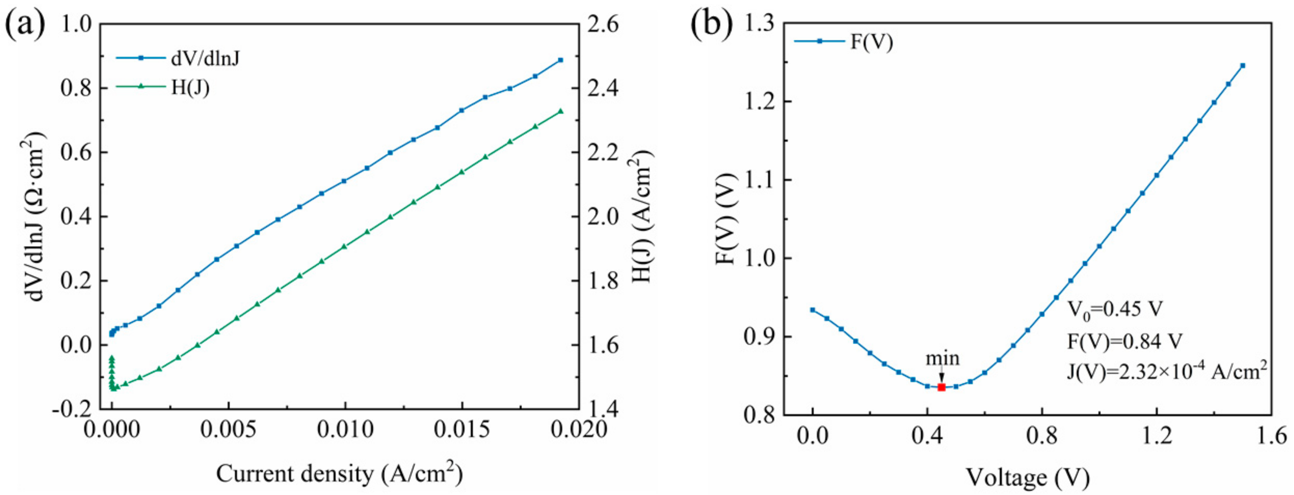
based on Equation (8), through the linear fitting ()- curve shown in Figure 5a (blue dot-line curve), the n and Rs of the Schottky diode are estimated to be 1.67 and 45.5 Ω cm2. Then, according to the Equation (9), and Rs of the Schottky diode could be obtained as 0.86 eV and 46.6 Ω cm2, by fitting the H(J)-J curve displayed in Figure 5a (green dot-line curve). In addition, according to the energy band diagram in Figure 3, can be demonstrated as [18], where and are the conduction minimum and Fermi level of the Ga2O3. , where is effective state density at conduction band, expressed as , thus the electron concentration of the Ga2O3 can be calculated to be 1.04 1019 cm−3 [25]. What’s more, based on the Norde’s method [26], a function F(V) is defined as:
so, and Rs could be expressed as:
and
where is the voltage at the rock bottom of this function, and are the corresponding functions of . As shown in Figure 5b, the has been marked as 0.45 V. On the basis of Equations (10)–(12), and Rs of the Schottky diode could be obtained as 1.04 eV and 112.1 Ω cm2.
The Schottky barrier region in a Schottky diode could be regarded as a planar capacitance, which can be shown as [25,27], where W is the width of the depletion, and are the permittivity of Ga2O3 (~10) and vacuum permittivity (8.85 10−12 F/m). Based on Poisson’s equation, it can be described as:
As shown in Figure 6a, the capacitance–voltage (C–V) and -V curves are displayed with a frequency (f) of 100 kHz, and it can be clearly seen that the C decreases from 1.75 10−10 F to 1.27 10−10 F, with a gradual slowing rate. With Equation (13), the Nd could be fitted through the -V curve to be 4.36 1017 cm−3. In addition to Figure 6b, the C is almost unchanged with different frequencies, due to the fact that the current in a Schottky diode is caused by the entrance of a majority carrier into the metal side instead of the charge accumulation, i.e., there is no storage effect, thus no diffusion capacitance. Such characterization is beneficial in constructing high-frequency devices for Ga2O3.
Table 2 lists and compares the basic electrical parameters of some Ga2O3 SBDs in the past two years. From the table, we comprehensively discussed and calculated the basic electrical parameters by different analysis methods of J–V and C–V.
4. Conclusions
In this work, an EFG-grown Ni/Ga2O3/Ti Schottky diode is fabricated and characterized. By different analysis methods of J–V and C–V, its electrical parameters such as on-state resistance (Ron), Schottky barrier height (), the ideal factor (n), series resistance (Rs) and the carrier concentration (Nd) are obtained and discussed, systematically and comprehensively. The further investigation of Ga2O3 materials and devices is in inherent demand due to its excellent properties and the prospect of applications.
Author Contributions
S.Z.: methodology, validation, formal analysis, investigation, writing–original draft. Z.L.: conceptualization, methodology, resources, writing–original draft, funding acquisition. Y.L.: validation, investigation. Y.Z., P.L., Z.W.: project administration, funding acquisition. W.T.: supervision, project administration, funding acquisition. All authors have read and agreed to the published version of the manuscript.
Funding
This work was supported by the National Natural Science Foundation of China (Grant No. 61774019), BUPT Excellent Ph.D. Students Foundation (Grant No. CX2020314), the Fund of State Key Laboratory of Information Photonics and Optical Communications (Beijing University of Posts and Telecommunications, Beijing, China), and the Fundamental Research Funds for the Central Universities, China.
Conflicts of Interest
The authors declare that they have no known competing financial interests or personal relationships that could have appeared to influence the work reported in this paper.
References
- Liu, Z.; Li, P.; Zhi, Y.; Wang, X.; Chu, X.; Tang, W. Review of gallium oxide based field-effect transistors and Schottky barrier diodes. Chin. Phys. B 2019, 28, 017105. [Google Scholar] [CrossRef]
- Zhang, H.; Yuan, L.; Tang, X.; Hu, J.; Sun, J.; Zhang, Y.; Zhang, Y.; Jia, R. Progress of ultra-wide band-gap Ga2O3 semiconductor materials in power MOSFETs. IEEE Trans. Power Electron. 2020, 35, 5157. [Google Scholar] [CrossRef]
- Qin, Y.; Long, S.; Dong, H.; He, Q.; Jian, G.; Zhang, Y.; Hou, X.; Tan, P.; Zhang, Z.; Lv, B.; et al. Review of deep ultraviolet photodetector based on gallium oxide. Chin. Phys. B 2019, 28, 018501. [Google Scholar] [CrossRef]
- Yang, J.; Ren, F.; Tadjer, M.; Pearton, S.J.; Kuramata, A. 2300 V Reverse Breakdown Voltage Ga2O3 Schottky Rectifiers. ECS J. Solid State Sci. Technol. 2018, 7, Q92. [Google Scholar] [CrossRef]
- Hu, Z.; Zhou, H.; Feng, Q.; Zhang, J.; Zhang, C.; Dang, K.; Cai, Y.; Feng, Z.; Gao, Y.; Kang, X.; et al. Field-Plated Lateral β-Ga2O3 Schottky Barrier Diode With High Reverse Blocking Voltage of More Than 3 kV and High DC Power Figure-of-Merit of 500 MW/cm2. IEEE Electron Device Lett. 2018, 39, 1564. [Google Scholar] [CrossRef]
- Liang, S.; Sheng, H.; Liu, Y.; Huo, Z.; Lu, Y.; Shen, H. ZnO Schottky ultraviolet photodetectors. J. Cryst. Growth 2001, 225, 110. [Google Scholar] [CrossRef]
- Liu, Z.; Wang, X.; Liu, Y.; Guo, D.; Li, S.; Yan, Z.; Tan, C.-K.; Li, W.; Li, P.; Tang, W. A high-performance ultraviolet solar-blind photodetector based on a β-Ga2O3 Schottky photodiode. J. Mater. Chem. C 2019, 7, 13920. [Google Scholar] [CrossRef]
- Qin, Y.; Sun, H.; Long, S.; Tompa, G.S.; Salagaj, T.; Dong, H.; He, Q.; Jian, G.; Liu, Q.; Lv, H.; et al. High-Performance Metal-Organic Chemical Vapor Deposition Grown ε-Ga2O3 Solar-Blind Photodetector With Asymmetric Schottky Electrodes. IEEE Electron Device Lett. 2019, 40, 1475. [Google Scholar] [CrossRef]
- Chen, N.; Ma, J.; Li, P.; Xu, H.; Liu, Y. Zero-biased deep ultraviolet photodetectors based on graphene/cleaved (100) Ga2O3 heterojunction. Opt. Express 2019, 27, 8717. [Google Scholar] [CrossRef]
- Chen, Y.; Zhang, K.; Yang, X.; Chen, X.; Sun, J.; Zhao, Q.; Li, K.; Shan, C. Solar-blind photodetectors based on MXenes–β-Ga2O3 Schottky junctions. J. Phys. D Appl. Phys. 2020, 53, 48400. [Google Scholar] [CrossRef]
- Alema, F.; Hertog, B.; Mukhopadhyay, P.; Zhang, Y.; Mauze, A.; Osinsky, A.; Schoenfeld, W.V.; Speck, J.S.; Vogt, T. Solar blind Schottky photodiode based on an MOCVD-grown homoepitaxial β-Ga2O3 thin film. APL Mater. 2019, 7, 022527. [Google Scholar] [CrossRef] [Green Version]
- Ma, N.; Tanen, N.; Verma, A.; Guo, Z.; Luo, T.; Xing, H.G.; Jena, D. Intrinsic electron mobility limits in β-Ga2O3. Appl. Phys. Lett. 2016, 109, 212101. [Google Scholar] [CrossRef] [Green Version]
- Zhang, F.; Arita, M.; Wang, X.; Chen, Z.; Saito, K.; Tanaka, T.; Nishio, M.; Motooka, T.; Guo, Q. Toward controlling the carrier density of Si doped Ga2O3 films by pulsed laser deposition. Appl. Phys. Lett. 2016, 109, 102105. [Google Scholar] [CrossRef]
- Kang, Y.; Krishnaswamy, K.; Peelaers, H.; Van de Walle, G. Fundamental limits on the electron mobility of β-Ga2O3. J. Phys. Condens. Matter 2017, 29, 234001. [Google Scholar] [CrossRef] [PubMed]
- Yadav, M.K.; Mondal, A.; Das, S.; Sharma, S.K.; Bag, A. Impact of Annealing Temperature on Band-alignment of PLD Grown Ga2O3/Si (100) Heterointerface. J. Alloys Compd. 2019, 819, 153502. [Google Scholar] [CrossRef]
- Yang, H.; Qian, Y.D.; Zhang, C.; Wuu, D.S.; Talwar, D.N.; Lin, H.H.; Lee, J.F.; Wan, L.Y.; He, K.Y.; Feng, Z.C. Surface/structural characteristics and band alignments of thin Ga2O3 films grown on sapphire by pulse laser deposition. Appl. Surf. Sci. 2019, 479, 1246. [Google Scholar] [CrossRef]
- Winkler, N.; Wibowo, R.A.; Kautek, W.; Ligorio, G.; List-Kratochvil, E.J.; Dimopoulos, T. Nanocrystalline Ga2O3 films deposited by spray pyrolysis from water-based solutions on glass and TCO substrates. J. Mater. Chem. C 2019, 7, 69. [Google Scholar] [CrossRef] [Green Version]
- Tung, R.T. The physics and chemistry of the Schottky barrier height. Appl. Phys. Rev. 2014, 1, 011304. [Google Scholar]
- He, H.; Orlando, R.; Blanco, M.A.; Pandey, R.; Amzallag, E.; Baraille, I.; Rerat, M. First-principles study of the structural, electronic, and optical properties of Ga2O3 in its monoclinic and hexagonal phases. Phys. Rev. B 2006, 74, 195123. [Google Scholar] [CrossRef] [Green Version]
- Eastman, D.E. Photoelectric Work Functions of Transition, Rare-Earth, and Noble Metals. Phys. Rev. B 1970, 2, 1. [Google Scholar] [CrossRef]
- Mohamed, M.; Irmscher, K.; Janowitz, C.; Galazka, Z.; Manzke, R.; Fornari, R. Schottky barrier height of Au on the transparent semiconducting oxide β-Ga2O3. Appl. Phys. Lett. 2012, 101, 132106. [Google Scholar] [CrossRef]
- Schottky, W.Z. Halbleitertheorie der Sperrschicht- und Spitzengleichrichter. Eur. Phys. J. A 1939, 113, 367. [Google Scholar] [CrossRef]
- Mott, N.F. The Theory of crystal rectifiers. Proc. R. Soc. A 1939, 171, 27. [Google Scholar]
- Cheung, S.K.; Cheung, N.W. Extraction of Schottky diode parameters from forward current-voltage characteristics. Appl. Phys. Lett. 1986, 49, 85. [Google Scholar] [CrossRef]
- Pierret, R.F. Semiconductor Device Fundamentals; Publishing House of Electronics Industry: Beijing, China, 1996. [Google Scholar]
- Norde, H. A modified forward IV plot for Schottky diodes with high series resistance. J. Appl. Phys. 1979, 50, 5052. [Google Scholar] [CrossRef]
- Ji, M.; Taylor, N.R.; Kravchenko, I.; Joshi, P.; Aytug, T.; Cao, L.R.; Paranthaman, M.P. Demonstration of Large-Size Vertical Ga2O3 Schottky Barrier Diodes. IEEE Trans. Power Electron. 2021, 36, 41. [Google Scholar] [CrossRef]
- Xu, Y.; Chen, X.; Cheng, L.; Ren, F.F.; Zhou, J.J.; Bai, S.; Lu, H.; Gu, S.L.; Zhang, R.; Zheng, Y.D.; et al. High performance lateral Schottky diodes based on quasi-degenerated Ga2O3. Chin. Phys. B 2019, 28, 038503. [Google Scholar] [CrossRef]
- Yuan, H.; Su, J.; Guo, R.; Tian, K.; Lin, Z.H.; Zhang, J.C.; Chang, J.J.; Hao, Y. Contact barriers modulation of graphene/β- Ga2O3 interface for high-performance Ga2O3 devices. Appl. Surf. Sci. 2020, 527, 146740. [Google Scholar] [CrossRef]
- Li, W.S.; Saraswat, D.; Long, Y.; Kazuki, N.; Jena, D.; Xing, H.G. Near-ideal reverse leakage current and practical maximum electric field in β- Ga2O3 Schottky barrier diodes. Appl. Phys. Lett. 2020, 116, 192101. [Google Scholar] [CrossRef]
- Reddy, P.S.; Janardhanam, V.; Shim, K.H.; Reddy, V.R.; Lee, S.N.; Park, S.J.; Choi, C.J. Temperature-dependent Schottky barrier parameters of Ni/Au on n-type (001) β-Ga2O3 Schottky barrier diode. Vacuum 2020, 171, 109012. [Google Scholar] [CrossRef]
Figure 1.
(a) The geometry of the Schottky diodes with structure. (b) Optical microscopy image of the fabricated Schottky diode.
Figure 1.
(a) The geometry of the Schottky diodes with structure. (b) Optical microscopy image of the fabricated Schottky diode.

Figure 2.
(a) The X-ray diffraction (XRD) pattern and (b) the X-ray photoelectron spectroscopy (XPS) of the Ga2O3 substrate, of which the scanning electron microscope (SEM) image is shown in (a) inset.
Figure 2.
(a) The X-ray diffraction (XRD) pattern and (b) the X-ray photoelectron spectroscopy (XPS) of the Ga2O3 substrate, of which the scanning electron microscope (SEM) image is shown in (a) inset.

Figure 3.
(a) The current density–voltage (J–V) curves of the Ni/Ga2O3/Ti Schottky diode, inset is the equivalent circuit diagram, (b) the n, Js, and Vbi based on thermionic emission (TE) model.
Figure 3.
(a) The current density–voltage (J–V) curves of the Ni/Ga2O3/Ti Schottky diode, inset is the equivalent circuit diagram, (b) the n, Js, and Vbi based on thermionic emission (TE) model.

Figure 4.
The energy band diagram of the Ni/Ga2O3/Ti Schottky diode (a) before and (b) after contact.
Figure 4.
The energy band diagram of the Ni/Ga2O3/Ti Schottky diode (a) before and (b) after contact.

Figure 5.
(a) The ()- and H(J)-J curve, (b) F(V)-V curves of the Schottky diode.

Figure 6.
(a) The C–V and -V curves, (b) the C–V curves with different frequency.


Table 1.
Comparison of the binding energies of Ga 2p1/2, Ga 2p3/2, and O 1s.
| Ga 2p1/2 (eV) | Ga 2p3/2 (eV) | O 1s (eV) | Reference |
|---|---|---|---|
| 1144.7 | 1117.9 | 530.6 | This work |
| 1145.18 | 1118.28 | 531.18 | [15] |
| 1145 | 1120 | 530.7 | [16] |
| 1145.5 | 1118.5 | 531.4 | [17] |
Table 2.
Basic performance parameters of some reported Ga2O3 Schottky diodes in 2019 and 2020.
| Substrate | Anode Metal | n | Ref | |||||||
|---|---|---|---|---|---|---|---|---|---|---|
| Wafer (100) | Ni | - | 2.44 105 | 1.34 | 0.52 | 0.93 | 51.5 | 45.5 | This work | |
| Epi layer (001) | Ni | 261 | - | 1.21 | 0.74 | - | 77.3 | - | [27] | |
| Wafer | Ni | 23 | 1.21 | 1.31–1.64 | 1.54 | - | [28] | |||
| Film (100) | Mo | 260 | - | - | - | 1.55 | - | - | [29] | |
| Wafer | Ni/Pt | - | - | 1.14 | 1.3 | 1.37 | - | - | [30] | |
| Epi layer (001) | Ni | - | 1.17 | - | 1.02 | 40 | - | [31] |
Publisher’s Note: MDPI stays neutral with regard to jurisdictional claims in published maps and institutional affiliations. |
© 2021 by the authors. Licensee MDPI, Basel, Switzerland. This article is an open access article distributed under the terms and conditions of the Creative Commons Attribution (CC BY) license (http://creativecommons.org/licenses/by/4.0/).
Share and Cite
MDPI and ACS Style
Zhang, S.; Liu, Z.; Liu, Y.; Zhi, Y.; Li, P.; Wu, Z.; Tang, W. Electrical Characterizations of Planar Ga2O3 Schottky Barrier Diodes. Micromachines 2021, 12, 259. https://0-doi-org.brum.beds.ac.uk/10.3390/mi12030259
AMA Style
Zhang S, Liu Z, Liu Y, Zhi Y, Li P, Wu Z, Tang W. Electrical Characterizations of Planar Ga2O3 Schottky Barrier Diodes. Micromachines. 2021; 12(3):259. https://0-doi-org.brum.beds.ac.uk/10.3390/mi12030259
Chicago/Turabian StyleZhang, Shiyu, Zeng Liu, Yuanyuan Liu, Yusong Zhi, Peigang Li, Zhenping Wu, and Weihua Tang. 2021. "Electrical Characterizations of Planar Ga2O3 Schottky Barrier Diodes" Micromachines 12, no. 3: 259. https://0-doi-org.brum.beds.ac.uk/10.3390/mi12030259
Note that from the first issue of 2016, this journal uses article numbers instead of page numbers. See further details here.