
Self-Assembled Monolayers: Versatile Uses in Electronic Devices from Gate Dielectrics, Dopants, and Biosensing Linkers


Department of Electronic Engineering, Gachon University, Seongnam 13120, Korea
*
Author to whom correspondence should be addressed.
Micromachines 2021, 12(5), 565; https://0-doi-org.brum.beds.ac.uk/10.3390/mi12050565
Submission received: 29 March 2021
/
Revised: 11 May 2021
/
Accepted: 14 May 2021
/
Published: 17 May 2021
(This article belongs to the Special Issue Doping Techniques in Emerging Semiconductors and Devices)
Abstract
:Self-assembled monolayers (SAMs), molecular structures consisting of assemblies formed in an ordered monolayer domain, are revisited to introduce their various functions in electronic devices. SAMs have been used as ultrathin gate dielectric layers in low-voltage transistors owing to their molecularly thin nature. In addition to the contribution of SAMs as gate dielectric layers, SAMs contribute to the transistor as a semiconducting active layer. Beyond the transistor components, SAMs have recently been applied in other electronic applications, including as remote doping materials and molecular linkers to anchor target biomarkers. This review comprehensively covers SAM-based electronic devices, focusing on the various applications that utilize the physical and chemical properties of SAMs.
1. Introduction
Self-assembled monolayers (SAMs) have been used extensively because of their great advantages, which include molecular assembly, spontaneous formation, and formation by immersion of the substrate in a solution with the precursor molecules [1,2,3]. SAMs are composed of a head group that binds to the surface, an end group that determines the surface’s characteristics after SAM treatment, and a spacer group that connects the head and end groups. The head group includes silane, phosphonic acid, and thiol, and the end group includes amine, methyl, and thiol. The spacer group mainly consists of alkyl carbon chains. Through molecular assembly, SAMs form an extremely strong molecule–substrate interaction, whereby chemical bonds are clearly formed at the interface. Owing to these powerful chemical interactions, SAMs can be used in several applications, especially in electronics that require an ordered domain of chemical components. Electronic devices have been developed comprehensively. To functionalize electronic devices, surface treatments are used to alter the interface between the layers to produce hydrophobic, hydrophilic, or specific molecular surfaces. This review provides an overview of the key contributions of SAMs to electronic devices taking into consideration three main aspects: (1) dielectrics, dielectric interfaces, or the semiconductor itself; (2) dopants to control the device’s properties; and (3) linkers to anchor analytics for biosensors.
2. SAMs as Basic Elements of the Device
In the first section, we comprehensively recapitulate the important advances of SAMs in organic thin-film transistors (OTFTs) [4,5,6,7,8]. Since 1990, OTFTs have emerged as soft electronic devices with functional properties that include mechanical flexibility [9,10,11,12,13] and a solution-processed, facile manufacturing process [14,15]. However, the organic semiconductors in OTFTs are vulnerable to charge traps [16,17,18] and leakage current, which frequently occur in oxide dielectrics (i.e., silicon dioxide (SiO2) [19,20,21], aluminum oxide (Al2O3) [22,23], and hafnium oxide (HfO2) [24]). Owing to the strong susceptibility of organic semiconductors to charge traps, OTFTs suffer from instability, which causes current–voltage sweep hysteresis [25,26,27], shifts in the threshold voltage (VTH) [28,29], and bias stress effects [30,31,32,33]. To address these issues, the treatment of the hydroxylated surfaces of dielectrics is crucial. SAMs exhibit appropriate properties to resolve these hydroxyl dielectric–organic semiconductor interface limitations. As SAMs have a Janus structure, a head group on one side and a tail group on the other [34], reactions with SAMs enable a dramatic change in the properties of a film surface. For example, a silane-based SAM contains a Si-O-H head group that can react with a hydroxyl group on the substrate, forming a covalent R-Si-O-substrate bond [35,36]. Through this mechanism, the dielectric surface can be altered to one that is desirable for the stable and robust operation of OTFTs. Furthermore, SAMs act as dielectrics or semiconductors in OTFTs.
2.1. SAM Treatment on SiO2 Gate Dielectrics
SiO2 has a large energy bandgap of ~9 eV and is used as a gate dielectric in most electronic devices owing to its excellent insulating properties. However, the many hydroxyl groups present on the surface of SiO2 can act as traps at the interface with the semiconductor layer. Therefore, if the gate dielectric SiO2 film is not controlled, the electrical hysteresis caused by the trap can lead to problems, such as operation failures of the electronic device, which must be solved. Based on this, many researchers have studied the use of SAMs as a surface treatment for SiO2.
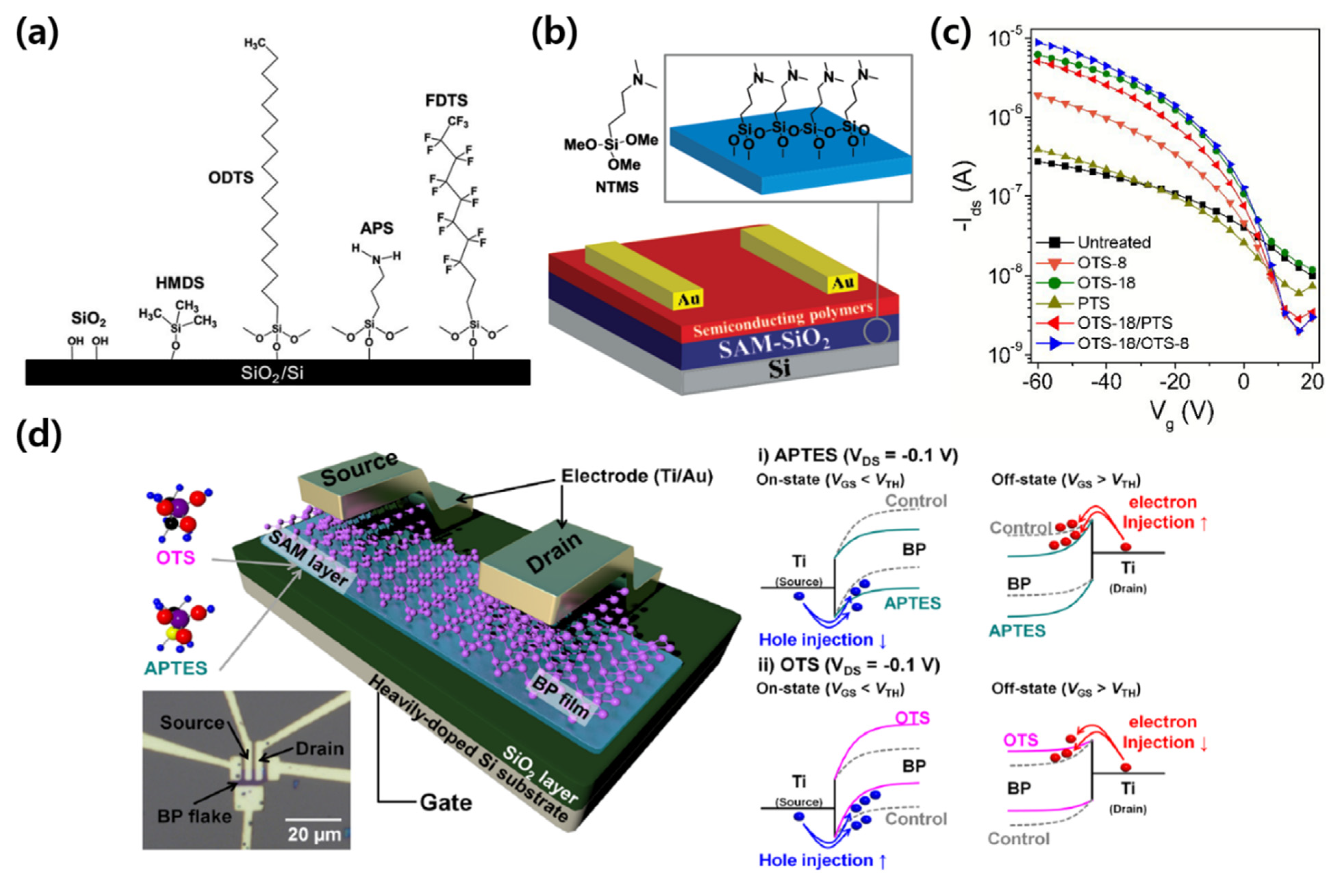
Ku et al. fabricated a graphene field effect transistor (FET), in which several functional group SAMs were applied as buffer layers, and analyzed the effect of each SAM (Figure 1a) [37]. Among them, the graphene FET on 1H,1H,2H,2H-perfluorodecyltriethoxysilane (FDTS)-treated SiO2 showed a p-doping effect, whereas for the (3-aminopropyl) triethoxysilane (APTES)-treated SiO2, an n-doping effect was observed. These results suggest that it is important to control the influence of the SAM dipole in the fabrication of graphene FETs. Wang et al. reported that the performance of an n-type polymer pSNT transistor was improved by treating the SiO2 surface with [3-(N,N-dimethylamino) propyl] trimethoxysilane (NTMS), an amine-tailed SAM (Figure 1b) [38]. The SiO2 surface treatment improved the low on/off current ratio characteristic due to the hole current in the off state by a factor of 10. Lei et al. studied the optimal surface treatment for SiO2 used in OFETs by using octyltrichlorosilane (OTS), octadecyltrichlorosilane (ODTS), and phenyltrichlorosilane (PTS) as treatments (Figure 1c) [39]. When using the ODTS treatment, high mobility characteristics appeared, but a low on/off current ratio was observed owing to the high off current. In contrast, when using the OTS and PTS treatments, high on/off current ratio characteristics but low mobility characteristics were obtained. Therefore, a combination of ODTS, with high mobility characteristics, and OTS or PTS, with a high on/off current ratio, was applied. As a result, both high mobility characteristics and high on/off current ratio characteristics were achieved. Kang et al. reported the p-type and n-type doping of black phosphorus (BP) films on SiO2 substrates treated with ODTS and APTES, respectively (Figure 1d) [40]. They suggested that this is because the energy band structure of BP was changed by the dipole of the APTES and ODTS functional groups. In addition, the APTES and ODTS functional groups affected the optical characteristics. For the BP transistor on the APTES-treated SiO2, the photocurrent generated under light irradiation was reduced compared to that on the untreated SiO2. In contrast, for the BP transistor on the ODTS-treated SiO2, the photocurrent increased.
2.2. SAM Treatment on Al2O3 Gate Dielectrics
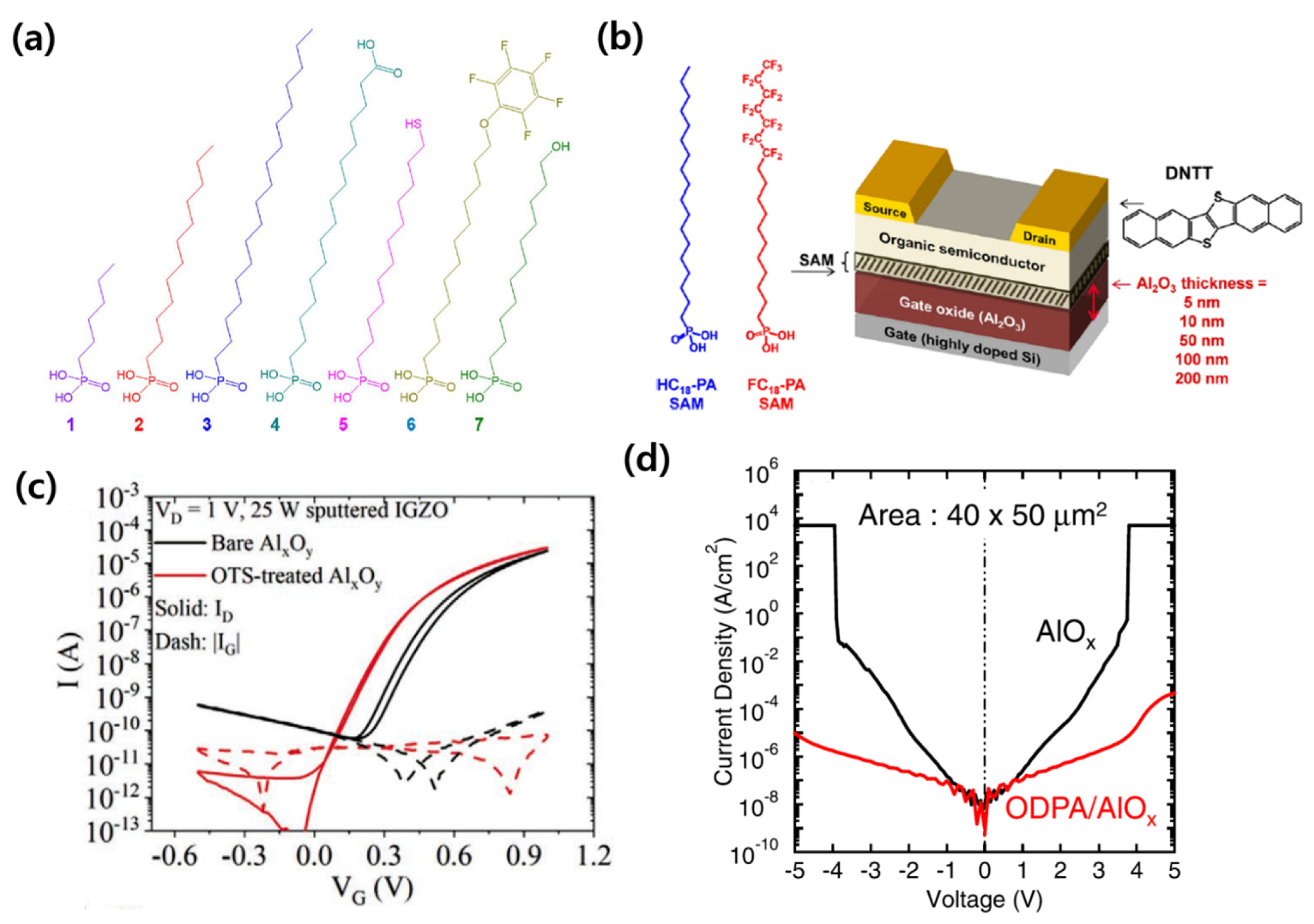
In addition to the SAM treatment on SiO2, many advances of SAM-treated Al2O3 have been reported. Jang et al. treated the hydrophilic surface of Al2O3 with various phosphonic acid SAMs and compared the characteristics based on the alkyl chain length and functional end groups of the SAMs (Figure 2a) [41]. The longer the alkyl chain length, the more hydrophobic the surface, resulting in greater contact angle characteristics. The characteristics of phosphonic acid SAM according to functional end-groups were identified as phosphonohexadecanoic acid (PHDA), 12-mercaptododecylphosphonic acid (MDPA), 12-pentafluorophenoxydodecylphosphonic acid (PFPA), and 11-hydroxyundecylphosphonic acid (HUPA). Among these phosphonic acid SAMs, only PFPA, which has a non-polar functional end-group, exhibited hydrophobic properties similar to alkyl phosphate SAMs. It was established that PHDA, MDPA, and HUPA have high surface energy characteristics because their functional end-groups are polar. Aghamohammadi et al. investigated the relationship between the gate dielectric thickness and the threshold voltage of n-octadecylphosphonic acid (ODPA)- and 12,12,13,13,14,14,15,15,16,16,17,17,18,18,18-pentadecylfluoro-octadecylphosphonic acid (FDPA)-treated Al2O3 in DNTT transistors (Figure 2b) [42]. In the case of FDPA, when the Al2O3 thickness increased, the threshold voltage showed an inverse relationship with the dielectric capacitance. In contrast, for the ODPA-treated Al2O3, the threshold voltage was determined only by the SAM, regardless of the thickness of the Al2O3. Therefore, they suggested that the shift in threshold voltage for the SAM-treated gate dielectric was related not only to the dipole of the SAM material, but also to the interface between the SAM material and the semiconductor layer. Kawanago et al. analyzed the changes when ODTS-treated Al2O3 was applied as the gate dielectric of an oxide semiconductor-based transistor (Figure 2c) [43]. After the ODTS treatment, as the density of the trap between the channel and the gate dielectric decreased, the carrier mobility and on/off current ratio increased. Cai et al. used an ODPA-treated Al2O3 gate for the low-voltage operation of MoS2 [44]. The gate leakage current was significantly reduced by the ODPA treatment (Figure 2d).
2.3. SAM Treatment on HfO2 Gate Dielectrics
As another high-k dielectric layer, HfO2 dielectric was applied by SAM treatments. Acton et al. showed that the performance of a low-voltage OTFT can be controlled by adjusting the carbon chain length of the alkyl PA SAM on the HfO2 insulating layer (Figure 3a) [45]. It was suggested that the high carrier mobility was determined by the balance between the SAMs that exhibited sufficient thickness and the disordered SAMs to prevent adverse effects in the high-k gate dielectric. Kim et al. introduced hydrophobic properties on the hydrophilic HfO2 surface by incorporating OH groups through OTS, ODTS, and n-dodecylphosphonic acid (DDPA) (Figure 3b) [46]. With this, they produced a poly-(2,5-bis(2-decyltetradecyl)-3-(3″,4′-difluoro-[2,2′:5′,2″-terthiophen]-5-yl)-6-(thiophen-2-yl) pyrrolo [3,4-c] pyrrole-1,4-(2H,5H)-dione) (PDPP2DT-T2)-based organic transistor capable of low voltage operation (<−4 V) with reduced trap density. Ting et al. studied the effects of SAMs containing different binding groups, such as ODPA, 4,5-dioctadecyl-benzene1,2-diol (C36C), 4-Octadecyl-benzene-1,2-diol (C18C), and stearic acid (SA) [47]. Among the four SAMs, the ODPA treatment resulted in a low leakage current density and the largest contact angle with water. In addition, dialkylcatechol showed similar properties to ODPA, indicating that a catechol-based SAM is suitable for HfO2 surface treatment. Finally, they demonstrated a pentacene TFT capable of operating under −1.5 V with an improved on/off current ratio through HfO2 surface treatment (Figure 3c). Acton et al. fabricated a poly (2,5-bis(3-tetradecyl-5-(3-tetradecylthiophen-2-yl)thiophen-2-yl) thiazolo [5,4-d] thiazole) (PTzQT-14) TFT that is flexible and capable of low voltage operation using an ODPA-treated HfO2 insulating film [48]. The ODPA treatment reduced the gate leakage current (Figure 3d), and, above all, the flexible TFT can possibly be applied as a flexible and wearable low-voltage device capable of low voltage operation owing to the extreme thinness of the SAM material.
2.4. SAM as Gate Dielectrics
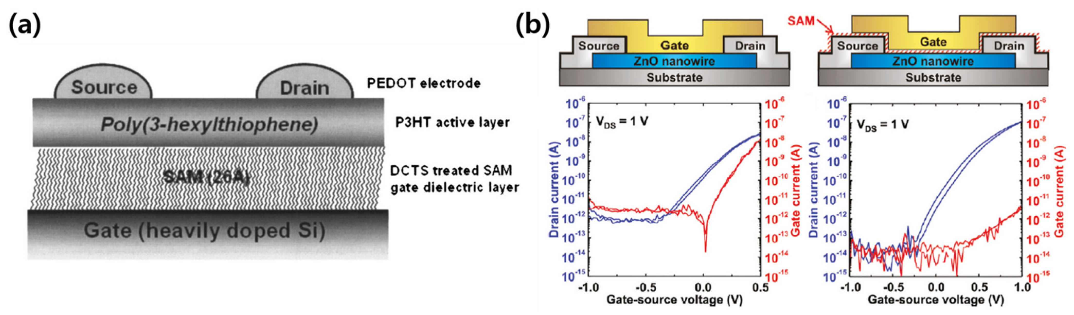
Since several SAMs themselves have good insulating properties, a low-voltage operation of the transistor by the SAM gate dielectric without an oxide dielectric was achieved. Halik et al. applied (18-phenoxyoctadecyl)trichlorosilane (PhO-OTS), a silane-based SAM material, as the gate dielectric of a pentacene TFT [49]. They applied the SAM gate dielectric in both a bottom-gate bottom-contact structure and a bottom-gate top-contact structure. In addition, the SAM gate dielectric, which is 2.5 nm thick, makes it possible to operate at voltages of less than 2 V. They also suggested that the SAM gate dielectric is capable of low-voltage and low-power operation, even in organic devices. A solution-processed poly(3-hexylthiophene) (P3HT) polymer transistor using a docosyltrichlorosilane (DCTS) SAM dielectric was demonstrated (Figure 4a) [50]. Kälblein et al. prepared a top-gate structure ZnO nanowire transistor in which ODPA, a phosphonic acid-based SAM material, was applied as the gate dielectric [51]. To confirm whether ODPA is effective as a gate dielectric, the electrical characteristics of the metal-semiconductor FET (MESFET) structure without the ODPA gate dielectric and the metal-insulator-semiconductor FET (MISFET) structure with the ODPA gate dielectric were compared (Figure 4b). The electrical characteristics of the MESFET structure without the ODPA gate dielectric and the MISFET structure with the ODPA gate dielectric were compared. The MESFET structure without the ODPA gate dielectric exhibited a high gate leakage current flow. However, the presence of the ODPA gate dielectric greatly reduced the gate leakage current, which improved the on/off current ratio. Therefore, the dielectric properties of ODPA were confirmed, and because of the thin thickness of the SAM, it was possible to operate the ZnO nanowire transistor at 1 V.
2.5. Self-Assembled Monolayer Field Effect Transistor (SAMFET)
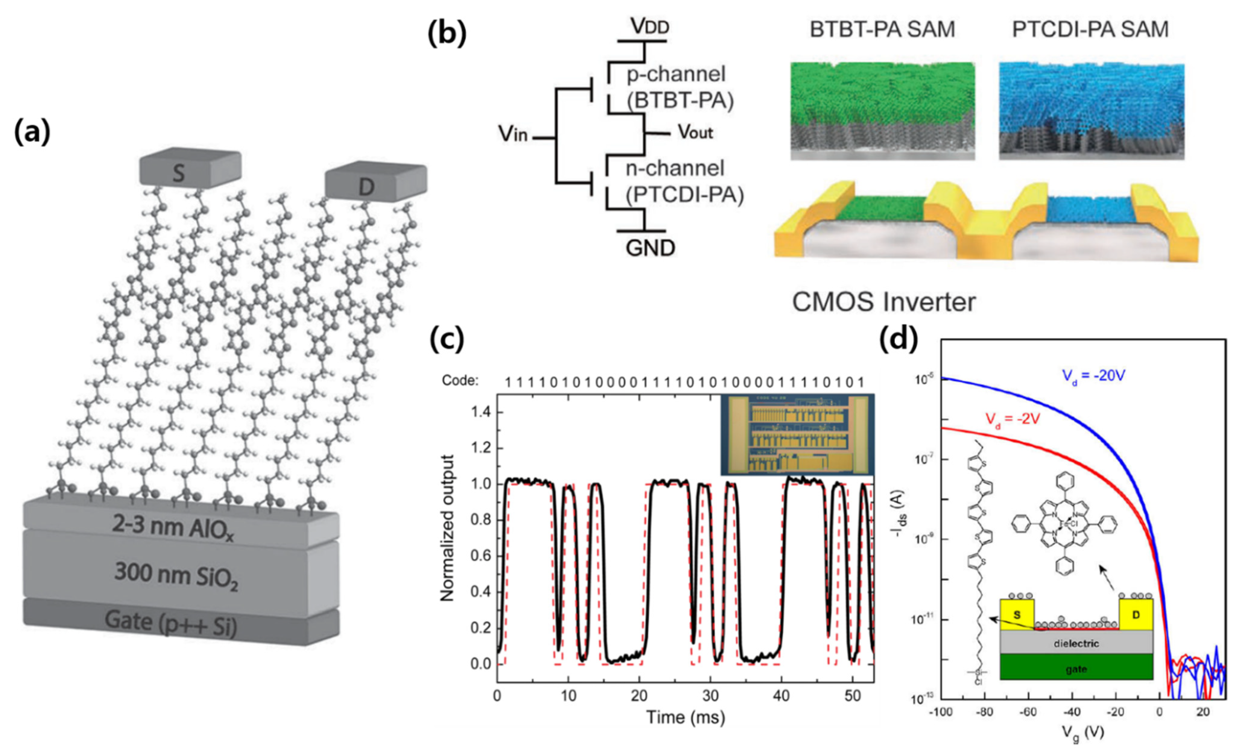
A self-aligned structure of SAMs enabled their operation as a semiconductor active layer through the π–π overlap in the molecular packing. Cernetic et al. fabricated a p-type SAMFET with (11-(5‴-(4-(methylthio)butyl)-[2,2′:5′,2″:5″,2‴-quaterthiophene]-5-yl)undecyl)phosphonic acid (MTB4TC11) and (12-(5‴-(4-(methylthio)butyl)-[2,2′:5′,2″:5″,2‴-quaterthiophene]-5-yl) dodecyl) phosphonic acid (MTB4TC12), which are phosphonic acid-based SAMs [52]. Figure 5a shows the schematic of the fabricated SAMFET. They improved the contact characteristics with the Au electrode by applying methylthiobutyl as a functional terminal group. In addition, the bonding between the SAM and the electrode was strengthened through annealing, so that the carrier mobility could be increased by more than 100-fold. By applying these optimized conditions, a SAMFET capable of low-voltage operation through a HfO2 gate dielectric was produced. Zhao et al. implemented two organic inverters using a SAMFET [53]. First, after fabricating an ambipolar transistor with a semiconducting SAM and a complementary semiconductor, they established a CMOS-like inverter with two anti-ambipolar transistors. Second, a CMOS inverter was produced by fabricating a benzothieno [3,2-b] [1] benzothiophene (BTBT)-PA-based p-type SAMFET and a 3,4,9,10-perylene tetracarboxylic diimide (PTCDI)-PA-based n-type SAMFET (Figure 5b). They presented the possibility of developing organic circuits by producing the aforementioned SAM-based organic inverters over a large area for the first time. Gholamrezaie et al. suggested that semiconducting SAMs can be grown on organic dielectrics and that charge transport is possible even at micrometer distances [54]. They also reported the use of a 4-bit code generator incorporating over 100 SAMFETs (Figure 5c). Andringa et al. reported the application of Fe(TPP)Cl as an NO receptor to a SAMFET and used it as a gas sensor (Figure 5d) [55]. They suggested that a very thin SAMFET channel, approximately one molecule thick, is suitable for use as a sensor.
3. SAMs as Dopants
In the second section, the effects of SAMs acting as dopants on the device’s properties are introduced. In the last decade, promising semiconductor materials, including transition metal dichalcogenides (TMDs) [56,57,58,59,60], oxides [61,62,63,64,65], and polymers [66,67,68,69,70], have emerged as next-generation semiconductors. However, the conventional doping techniques (i.e., ion implantation) used in silicon-based fabrications degrade and damage these semiconductors; thus, there is a need for the development of alternative methods to control the electrical properties of the semiconductors. To meet these demands, unusual SAM-based doping techniques have been attempted [71,72,73,74,75,76,77,78,79,80]. Owing to the ordered domain and large area coverage of SAMs, uniform and controllable doping was achieved. An expansive overview of SAM-based doping into oxides and TMDs is presented in this section.
3.1. Doping Effects of SAMs in Oxide Semiconductors
In recent years, the use of SAMs as a layer of remote doping material for prefabricated transistors, not as an insulating film or a semiconductor, has been attempted. As an example of this doping technique of an SAM on a metal oxide semiconductor, Cai et al. treated an IGZO surface with ODTS to form a passivation layer (Figure 6a), which greatly increased the carrier mobility [79]. In addition, without the passivation layer, the device significantly deteriorated after 1 year, whereas the device containing the passivation layer maintained its performance after 1 year (Figure 6b). This indicates that the passivation layer introduced through the SAM treatment protected the device from oxygen derivatives from the air over an extended period. Wan et al. improved electron mobility and the on/off current ratio through the 4-chlorobenzoic acid (PCBA) treatment of ZnO transistors (Figure 6c) [81]. They extracted the trap concentration from the electrical characteristics of a pristine ZnO transistor and a PCBA-treated ZnO transistor and found that it decreased by about 10-fold after PCBA treatment. Lee et al. studied the surface treatment of IGZO TFTs with SAMs [78]. The results showed that by selecting a SAM with an appropriate functional group polarity and alkyl chain length, the electron transport could be improved and the hysteresis reduced (Figure 6d). In addition, it was shown that the contact resistance can be controlled by the alkyl chain length when using the same functional group. A similar result was achieved by Xiao et al. for IGZO TFTs [75]. Xiao et al. analyzed the effect of passivating the surface of an IGZO TFT with triethoxysilane (TES)-based SAMs. In addition, three types of TESs containing different carbon chain lengths, namely methyltriethoxysilane (MTES), octyltriethoxysilane (OTES), and oxtadecyltriethoxysilane (ODTES), were used to determine the effect of the alkyl chain length on the semiconductor characteristics. As a result, the longer the alkyl chain length, the more improved all the electrical characteristics, such as carrier mobility and hysteresis.
3.2. Electrical Doping Effect of SAMs in 2D Materials
The SAM doping techniques were attempted in 2D TMDs. Due to the atomically thin nature of the TMDs, the SAM doping was more effective in improving device performance. Kang et al. reported improved electrical properties for MoS2 and WSe2 transistors by doping with ODTS and APTES SAM materials (Figure 7a) [72]. When the MoS2 transistors were doped with APTES and the WSe2 transistors with ODTS, the field-effect mobility increased by approximately fivefold. In contrast, when doping the MoS2 transistor with ODTS and the WSe2 transistor with APTES, the field-effect mobility deteriorated. As ODTS and APTES exhibited p-doped and n-doped effects, the n-type MoS2 could be improved by APTES doping, and the p-type WSe2 could be improved by ODTS doping. They also suggested that the p-doping effect of the ODTS-doped WSe2 transistor was owing to the functional group of the ODTS [73]. Due to the positive charges of the methyl functional groups (-CH3) in ODTS, the electrons in WSe2 are attracted to the junction with ODTS, which leads to a decrease in the concentration of electrons in the WSe2 channel and a p-doping effect (Figure 7b). Hasnain et al. studied the doping effect of (3-aminopropyl)trimethoxysilane (APTMS) in ReSe2 transistors with n-type characteristics as a function of the APTMS concentration (Figure 7c–e) [74]. They suggested that the electron concentration in the ReSe2 channel increased because of the negative charges of the amine functional groups (-NH2) of APTMS at the interface between APTMS and ReSe2. As a result, the n-doping effect of APTMS reduced the effective barrier height between ReSe2 and the electrode, and the threshold voltage shifted in the negative direction. After doping with APTMS, these effects increased the photoresponsivity for all wavelength bands, not only in terms of electrical characteristics, but also in terms of the photoresponsive properties.
4. Biosensor Linkers Based on SAMs
Finally, we revisit the recent advances and studies in biosensors that use SAM-based linkers. Recent viral diseases and pandemics have generated interest in various types of sensors, such as electrochemical impedance spectroscopy (EIS) [82,83,84] and field-effect biosensors (BioFETs) [85,86,87,88,89]. These devices can provide warnings on a patient’s dangerous condition or offer daily monitoring information. Biosensors should exhibit crucial functions, including fast detection and response [90], robust operation [91], and the detection of low-concentration targets [92], for reliable detection systems. To realize these functions, a linker with an ordered domain should be located between the active layer and the analytes to anchor the analytes (i.e., target antibodies and enzymes). As molecular assemblies allow SAMs to be tightly packed and oriented on the active layer, a dense domain of analytes can be formed. In this section, we provide an overview of biosensors for antigen and biomarker detection enhanced by using SAM-based linkers.
Kim et al. studied an extended gate FET (EGFET)-based biosensor for detecting streptavidin–biotin protein complexes [93]. The sequence of immobilization of streptavidin to the gate electrode is shown in Figure 8a. They used a C11-oligo(ethylene glycol)-terminated (OEG) thiol SAM with thiol and hydroxyl groups to immobilize streptavidin (SPV) on the Au gate electrode. The OEG thiol SAM head group thiols, was bonded to the Au gate electrode to form a hydroxyl group on the surface. Then, streptavidin was immobilized by combining the amine group of streptavidin with the surface’s hydroxyl group. Similarly, Lee et al. demonstrated a biosensor based on a high electron mobility transistor (HEMT) for C-reactive protein (CRP) detection by immobilizing the antibody on the gate [94]. To immobilize the receptor, CRP, a carboxyl group was first formed on the gate surface with 11-mercaptoundecanoic acid(11-MUA), and then a stable amine-reactive product was formed with N-(3-dimethylaminopropyl)-N′-ethylcarbodiimide hydrochloride (EDC) and N-hydroxysuccinimide (NHS). Then, CRP-antibody immobilization was completed. Figure 8b shows the AlGaN/GaN HEMT-based biosensor configuration for CRP detection. They detected CRP by measuring not only the change in drain current but also the change in the output voltage using a null-balancing circuit. In addition to immobilizing the receptor on the gate electrode, a method of immobilizing the receptor on the channel layer has also been reported. Liu et al. immobilized uricase on a ZnO nanowire channel to fabricate a sensor that detects uric acid [88]. Figure 8c shows the process of immobilizing uricase. First, the hydroxyl group on the ZnO nanowire surface was converted into an amine group by silane-based APTES treatment. Then, the surface modification was completed by linking the uricase and the amine group through glutaraldehyde. Gao et al. demonstrated a tunnel field-effect transistor (TFET)-based biosensor capable of detecting CYFRA21-1, a lung cancer biomarker [85]. They first formed amine groups on the Si nanowire channel by APTES treatment. Subsequently, the amine group on the Si nanowire surface was reacted with glutaraldehyde, and then the CYFRA21-1 antibody was immobilized. When the CYFRA21-1 antigen and antibody were combined, the electrical properties acting on the channel region was changed, influenced by the polarity of the biomolecule. The energy band structure of the TFET and the tunneling current were also modulated (Figure 8d). As a result, the presence of CYFRA21-1 antigen could be detected through the change of the current of the TFET. Shin et al. demonstrated a biosensor for detecting biomarkers related to liver health based on EIS [95]. Starting with the SAM treatment, the antibody’s binding process to the Au electrode is shown in Figure 8e. The Au electrode was treated with 11-MUA SAM, and NHS ester was formed through EDC/NHS. Then, SPV was immobilized by reacting the surface with the amine group of SPV. Finally, it was completed by immobilizing biotinylated antibodies (biot-Abs) to SPV. The detection of the target in the fabricated sensor was achieved through the change in impedance as shown in Figure 8f.
5. Summary
We first revisited examples of using SAM for the surface treatment of oxide gate dielectrics in electronics. Oxide dielectrics had problems due to charge traps caused by hydroxyl groups on the surface and problems with leakage current flowing in high-k dielectrics such as Al2O3 and HfO2. These problems in the oxide dielectric were addressed by the SAM; the SAMs reacting with the hydroxyl groups on the dielectric surface were treated. The increased hydrophobicity can improve device performance because it minimizes the absorption of oxygen or water molecules that result in poor device stability and performance degradation. As the SAM treatment reduced the charge trap by allowing the hydrophilic surface to become hydrophobic. The decrease in trap density led to improved electrical characteristics such as high on/off current ratio and the enhanced mobility of the devices. Besides, several researchers have experimentally proven that there is also an effect by the carbon chain of SAM. This is because the longer the carbon chain length is, the better the SAM molecules can be ordered and the more hydrophobic the surface is.
Interestingly, SAMs themselves are also used as gate dielectrics or semiconductor layers. Table 1 shows examples of applying SAMs to the gate dielectric surface treatment and examples of using a SAM itself as a gate dielectric. The possibility of applying a molecularly thin SAM as a gate dielectric mean that the device can be operated with low voltage. Based on these research results, this has been demonstrated for SAM gate dielectric- and SAMFET-based functional circuit-levels such as NANDs, ring oscillators, and code generators. This shows that SAMs have great potential in electronics.
The utility of SAMs is not limited to basic elements of devices such as gate dielectrics and semiconductors, but is also used as a dopant for devices. TMDs and oxide semiconductors, emerging as next-generation semiconductor materials, have difficulty applying the ion implantation process for doping conventional silicon semiconductors. As an alternative to the conventional doping method, which is difficult to apply, studies have been conducted to provide a doping effect by placing a SAM on a fabricated device. We have summarized examples of doping attempts using SAM in Table 2. The doping effect in oxide semiconductors and TMDs is slightly different. In oxide semiconductors, the hydroxyl group acting as a trap on the surface of the semiconductor layer decreases through reaction with the head group of the SAM, thereby eliminating the trapping sites and increasing the number of carriers in the channel, thereby improving the device performance [78]. On the other hand, in TMDs, the characteristics of the TMD-based transistor are modulated due to the effect of the tail group of the SAM facing the semiconductor layer, and the dipole of the tail group applies an electric field to the channel [71].
Finally, we dealt with the use of SAMs as a linker in biosensors. In biosensors, it is necessary to have selectivity for the specific target to be detected, such as an antigen, and the ability to detect if even a small concentration of the target is present is important. Therefore, it is necessary to allow the maximum interaction between the target and the receptor to occur. As a method, there is alignment by immobilizing receptors such as antibodies in a specific direction. However, since not all receptors can be directly immobilized on various substrates, SAMs are widely applied to connect and immobilize the substrate and the receptor as a linker.
As there are many advantages, shown through various examples, of using SAMs, further advances in electronics will be in progress. SAM-based electronic devices have the following merits and directions for future research: (1) low-cost, (2) device flexibility, (3) work-function modification, and (4) device stability enhancement. Owing to the solution processability of SAMs, the SAM-based device process can be performed through simple spin-coating or printing, which reduces the fabrication process complexity, and thus lowers the cost. Furthermore, the low thermal budget of the SAM-based process enhances the compatibility with flexible substrates (i.e., polyimide and polyethylene terephthalate). These merits provide great ease in implementing flexible devices such as communication devices and sensors [96,97]. In addition to the fabrication processing aspect, SAMs enable the contribution towards device aspects. The work function modification can be achieved by SAM surface treatment due to its molecularly thin thickness and assembly reaction. This property ensures that the work function of the electrodes matches what can provide the desired energy band junction for each device [98,99]. The SAMs also improve the device stability. The SAM can control surface properties into hydrophobicity, minimizing the absorption of oxygen or water molecules that act as charge trap sites. There are still difficulties such as the improvement of the integration process, miniaturization, and pattern refinement in SAM-based electronics. However, the advantages and possibilities of the aforementioned SAMs are expected to lead to the next generation of electronic devices.
Author Contributions
S.K. performed the literature research and analysis and wrote the paper. H.Y. initiated and supervised the work and wrote the paper. All authors have read and agreed to the published version of the manuscript.
Funding
This research was supported by a National Research Foundation of Korea (NRF) grant funded by the Korean Government (MSIT) (NRF-2020R1A2C1101647 and NRF-2020M3A9E4104385).
Conflicts of Interest
The authors declare no conflict of interest.
References
- Fox, H.; Zisman, W. The spreading of liquids on low energy surfaces. I. polytetrafluoroethylene. J. Colloid Sci. 1950, 5, 514–531. [Google Scholar] [CrossRef]
- Bain, C.D.; Whitesides, G.M. Modeling organic surfaces with self-assembled monolayers. Angew. Chem. 1989, 101, 522–528. [Google Scholar] [CrossRef]
- Bigelow, W.; Pickett, D.; Zisman, W. Oleophobic monolayers: I. Films adsorbed from solution in non-polar liquids. J. Colloid Sci. 1946, 1, 513–538. [Google Scholar] [CrossRef]
- Klauk, H. Organic thin-film transistors. Chem. Soc. Rev. 2010, 39, 2643–2666. [Google Scholar] [CrossRef] [PubMed]
- Horowitz, G.; Fichou, D.; Peng, X.; Garnier, F. Thin-film transistors based on alpha-conjugated oligomers. Synth. Met. 1991, 41, 1127–1130. [Google Scholar] [CrossRef]
- Haddon, R.; Perel, A.; Morris, R.; Palstra, T.; Hebard, A.; Fleming, R.M. C60 thin film transistors. Appl. Phys. Lett. 1995, 67, 121–123. [Google Scholar] [CrossRef] [Green Version]
- Torsi, L.; Dodabalapur, A.; Katz, H. An analytical model for short-channel organic thin-film transistors. J. Appl. Phys. 1995, 78, 1088–1093. [Google Scholar] [CrossRef]
- Peng, X.; Horowitz, G.; Fichou, D.; Garnier, F. All-organic thin-film transistors made of alpha-sexithienyl semiconducting and various polymeric insulating layers. Appl. Phys. Lett. 1990, 57, 2013–2015. [Google Scholar] [CrossRef]
- Kim, J.H.; Hong, S.H.; Seong, K.D.; Seo, S. Fabrication of Organic Thin-Film Transistors on Three-Dimensional Substrates Using Free-Standing Polymeric Masks Based on Soft Lithography. Adv. Funct. Mater. 2014, 24, 2404–2408. [Google Scholar] [CrossRef]
- Uno, M.; Isahaya, N.; Cha, B.-S.; Omori, M.; Yamamura, A.; Matsui, H.; Kudo, M.; Tanaka, Y.; Kanaoka, Y.; Ito, M.; et al. High-Yield, Highly Uniform Solution-Processed Organic Transistors Integrated into Flexible Organic Circuits. Adv. Electron. Mater. 2017, 3, 1600410. [Google Scholar] [CrossRef]
- Choi, H.H.; Yi, H.T.; Tsurumi, J.; Kim, J.J.; Briseno, A.L.; Watanabe, S.; Takeya, J.; Cho, K.; Podzorov, V. A large anisotropic enhancement of the charge carrier mobility of flexible organic transistors with strain: A Hall effect and Raman study. Adv. Sci. 2020, 7, 1901824. [Google Scholar] [CrossRef] [Green Version]
- Min, H.; Kang, B.; Shin, Y.S.; Kim, B.; Lee, S.W.; Cho, J.H. Transparent and colorless polyimides containing multiple trifluoromethyl groups as gate insulators for flexible organic transistors with superior electrical stability. ACS Appl. Mater. Interfaces 2020, 12, 18739–18747. [Google Scholar] [CrossRef]
- Kim, J.-H.; Liang, Y.; Seo, S. Patchable thin-film strain gauges based on pentacene transistors. Org. Electron. 2015, 26, 355–358. [Google Scholar] [CrossRef]
- Bischak, C.G.; Flagg, L.Q.; Ginger, D.S. Ion Exchange Gels Allow Organic Electrochemical Transistor Operation with Hydrophobic Polymers in Aqueous Solution. Adv. Mater. 2020, 32, 2002610. [Google Scholar] [CrossRef]
- Yoo, H.; Choi, H.H.; Shin, T.J.; Rim, T.; Cho, K.; Jung, S.; Kim, J.J. Self-Assembled, Millimeter-Sized TIPS-Pentacene Spherulites Grown on Partially Crosslinked Polymer Gate Dielectric. Adv. Funct. Mater. 2015, 25, 3658–3665. [Google Scholar] [CrossRef]
- Choi, C.G.; Bae, B.S. Effects of Hydroxyl Groups in Gate Dielectrics on the Hysteresis of Organic Thin Film Transistors. Electrochem. Solid State Lett. 2007, 10. [Google Scholar] [CrossRef] [Green Version]
- Gu, G.; Kane, M.G. Moisture induced electron traps and hysteresis in pentacene-based organic thin-film transistors. Appl. Phys. Lett. 2008, 92. [Google Scholar] [CrossRef]
- Lee, S.; Koo, B.; Shin, J.; Lee, E.; Park, H.; Kim, H. Effects of hydroxyl groups in polymeric dielectrics on organic transistor performance. Appl. Phys. Lett. 2006, 88. [Google Scholar] [CrossRef]
- Zhang, Y.; Ziegler, D.; Salmeron, M. Charge trapping states at the SiO2–oligothiophene monolayer interface in field effect transistors studied by Kelvin probe force microscopy. ACS Nano 2013, 7, 8258–8265. [Google Scholar] [CrossRef]
- Mathijssen, S.G.; Kemerink, M.; Sharma, A.; Cölle, M.; Bobbert, P.A.; Janssen, R.A.; de Leeuw, D.M. Charge Trapping at the Dielectric of Organic Transistors Visualized in Real Time and Space. Adv. Mater. 2008, 20, 975–979. [Google Scholar] [CrossRef]
- Chua, L.-L.; Zaumseil, J.; Chang, J.-F.; Ou, E.C.-W.; Ho, P.K.-H.; Sirringhaus, H.; Friend, R.H. General observation of n-type field-effect behaviour in organic semiconductors. Nature 2005, 434, 194–199. [Google Scholar] [CrossRef] [PubMed]
- McLean, F.B.; Boesch, H.E.; McGarrity, J.M.; Oswald, R.B. Rapid annealing and charge injection in Al2O 3 MIS capacitors. IEEE Trans. Nucl. Sci. 1974, 21, 47–55. [Google Scholar] [CrossRef]
- Zaininger, K.; Waxman, A. Radiation resistance of Al2O 3 MOS devices. IEEE Trans. Electron. Devices 1969, 16, 333–338. [Google Scholar] [CrossRef]
- Kawanago, T.; Ikoma, R.; Oba, T.; Takagi, H. Radical oxidation process for hybrid SAM/HfOx gate dielectrics in MoS2 FETs. In Proceedings of the 2017 47th European Solid-State Device Research Conference (ESSDERC), Leuven, Belgium, 11–14 September 2017; pp. 114–117. [Google Scholar]
- Lill, A.T.; Eftaiha, A.A.F.; Huang, J.; Yang, H.; Seifrid, M.; Wang, M.; Bazan, G.C.; Nguyen, T.Q. High-k fluoropolymer gate dielectric in electrically stable organic field-effect transistors. ACS Appl. Mater. Interfaces 2019, 11, 15821–15828. [Google Scholar] [CrossRef]
- Kwon, J.-H.; Choi, J.-H.; Bae, J.-H. Hysteresis reduction for organic thin film transistors with multiple stacked functional zirconia polymeric films. Crystals 2019, 9, 634. [Google Scholar] [CrossRef]
- Wang, H.; Yang, M.; Tong, Y.; Zhao, X.; Tang, Q.; Liu, Y. Manipulating the hysteresis via dielectric in organic field-effect transistors toward synaptic applications. Org. Electron. 2019, 73, 159–165. [Google Scholar] [CrossRef]
- Padma, N.; Sawant, S.N.; Sen, S. Study on post-deposition annealing influenced contribution of hole and electron trapping to threshold voltage stability in organic field effect transistors. Mater. Sci. Semicond. Process. 2015, 30, 18–24. [Google Scholar]
- Gomes, H.L.; Stallinga, P.; Dinelli, F.; Murgia, M.; Biscarini, F.; De Leeuw, D.M.; Muck, T.; Geurts, J.; Molenkamp, L.; Wagner, V. Bias-induced threshold voltages shifts in thin-film organic transistors. Appl. Phys. Lett. 2004, 84, 3184–3186. [Google Scholar] [CrossRef] [Green Version]
- Hong, S.; Yoo, H. Robust Molybdenum Diselenide Ambipolar Transistors with Fluoropolymer Interfacial Layer and Their Application to Complementary Inverter Circuits. J. Alloys Compd. 2021, 868, 159212. [Google Scholar] [CrossRef]
- Tang, W.; Zhao, J.; Huang, Y.; Ding, L.; Li, Q.; Li, J.; You, P.; Yan, F.; Guo, X. Bias stress stability improvement in solution-processed low-voltage organic field-effect transistors using relaxor ferroelectric polymer gate dielectric. IEEE Electron. Device Lett. 2017, 38, 748–751. [Google Scholar] [CrossRef]
- Park, S.; Kim, S.H.; Choi, H.H.; Kang, B.; Cho, K. Recent Advances in the Bias Stress Stability of Organic Transistors. Adv. Funct. Mater. 2020, 30, 1904590. [Google Scholar] [CrossRef]
- Jeong, J.W.; Hwang, H.S.; Choi, D.; Ma, B.C.; Jung, J.; Chang, M. Hybrid Polymer/Metal Oxide Thin Films for High Performance. Flex. Transistors Micromach. 2020, 11, 264. [Google Scholar] [CrossRef] [Green Version]
- Ulman, A. Self-assembled monolayers of alkyltrichiorosilanes: Building blocks for future organic materials. Adv. Mater. 1990, 2, 573–582. [Google Scholar] [CrossRef]
- Barriga, J.; Coto, B.; Fernandez, B. Molecular dynamics study of optimal packing structure of OTS self-assembled monolayers on SiO2 surfaces. Tribol. Int. 2007, 40, 960–966. [Google Scholar] [CrossRef]
- Tiao, H.-C.; Lee, Y.-J.; Liu, Y.-S.; Lee, S.-H.; Li, C.-H.; Kuo, M.-Y. Effect of hydroxyl density on condensation behaviors of self-assembled monolayers and performance of pentacene-base organic thin-film transistors. Org. Electron. 2012, 13, 1004–1011. [Google Scholar] [CrossRef]
- Ku, G.M.; Lee, E.; Kang, B.; Lee, J.H.; Cho, K.; Lee, W.H. Relationship between the dipole moment of self-assembled monolayers incorporated in graphene transistors and device electrical stabilities. RSC Adv. 2017, 7, 27100–27104. [Google Scholar] [CrossRef] [Green Version]
- Wang, Y.; Hasegawa, T.; Matsumoto, H.; Mori, T.; Michinobu, T. High-Performance n-Channel Organic Transistors Using High-Molecular-Weight Electron-Deficient Copolymers and Amine-Tailed Self-Assembled Monolayers. Adv. Mater. 2018, 30, 1707164. [Google Scholar] [CrossRef]
- Lei, Y.; Wu, B.; Chan, W.-K.E.; Zhu, F.; Ong, B.S. Engineering gate dielectric surface properties for enhanced polymer field-effect transistor performance. J. Mater. Chem. C 2015, 3, 12267–12272. [Google Scholar] [CrossRef]
- Kang, D.-H.; Jeon, M.H.; Jang, S.K.; Choi, W.-Y.; Kim, K.N.; Kim, J.; Lee, S.; Yeom, G.Y.; Park, J.-H. Self-Assembled Layer (SAL)-Based Doping on Black Phosphorus (BP) Transistor and Photodetector. ACS Photonics 2017, 4, 1822–1830. [Google Scholar] [CrossRef]
- Jang, S.; Son, D.; Hwang, S.; Kang, M.; Lee, S.-K.; Jeon, D.-Y.; Bae, S.; Lee, S.H.; Lee, D.S.; Kim, T.-W. Hybrid dielectrics composed of Al2O3 and phosphonic acid self-assembled monolayers for performance improvement in low voltage organic field effect transistors. Nano Converg. 2018, 5, 20. [Google Scholar] [CrossRef] [Green Version]
- Aghamohammadi, M.; Rödel, R.; Zschieschang, U.; Ocal, C.; Boschker, H.; Weitz, R.T.; Barrena, E.; Klauk, H. Threshold-Voltage Shifts in Organic Transistors Due to Self-Assembled Monolayers at the Dielectric: Evidence for Electronic Coupling and Dipolar Effects. ACS Appl. Mater. Interfaces 2015, 7, 22775–22785. [Google Scholar] [CrossRef]
- Cai, W.; Zhang, J.; Wilson, J.; Brownless, J.; Park, S.; Majewski, L.; Song, A. Significant Performance Improvement of Oxide Thin-Film Transistors by a Self-Assembled Monolayer Treatment. Adv. Electron. Mater. 2020, 6. [Google Scholar] [CrossRef] [Green Version]
- Kawanago, T.; Oda, S. Utilizing self-assembled-monolayer-based gate dielectrics to fabricate molybdenum disulfide field-effect transistors. Appl. Phys. Lett. 2016, 108. [Google Scholar] [CrossRef]
- Acton, O.; Ting, G.G.; Shamberger, P.J.; Ohuchi, F.S.; Ma, H.; Jen, A.K. Dielectric surface-controlled low-voltage organic transistors via n-alkyl phosphonic acid self-assembled monolayers on high-k metal oxide. ACS Appl. Mater. Interfaces 2010, 2, 511–520. [Google Scholar] [CrossRef]
- Kim, D.-K.; Lee, M.; Kim, B.; Choi, J.-H. Low-voltage, high-performance polymeric field-effect transistors based on self-assembled monolayer-passivated HfOx dielectrics: Correlation between trap density, carrier mobility, and operation voltage. Org. Electron. 2019, 74, 135–143. [Google Scholar] [CrossRef]
- Ting, G.G.; Acton, O.; Ma, H.; Ka, J.W.; Jen, A.K.-Y. Study on the Formation of Self-Assembled Monolayers on Sol—Gel Processed Hafnium Oxide as Dielectric Layers. Langmuir 2009, 25, 2140–2147. [Google Scholar] [CrossRef]
- Acton, O.; Osaka, I.; Ting, G.; Hutchins, D.; Ma, H.; McCullough, R.D.; Jen, A.K.Y. Phosphonic acid self-assembled monolayer and amorphous hafnium oxide hybrid dielectric for high performance polymer thin film transistors on plastic substrates. Appl. Phys. Lett. 2009, 95, 246. [Google Scholar] [CrossRef]
- Halik, M.; Klauk, H.; Zschieschang, U.; Schmid, G.; Dehm, C.; Schütz, M.; Maisch, S.; Effenberger, F.; Brunnbauer, M.; Stellacci, F. Low-voltage organic transistors with an amorphous molecular gate dielectric. Nature 2004, 431, 963–966. [Google Scholar] [CrossRef]
- Park, Y.D.; Kim, D.H.; Jang, Y.; Hwang, M.; Lim, J.A.; Cho, K. Low-voltage polymer thin-film transistors with a self-assembled monolayer as the gate dielectric. Appl. Phys. Lett. 2005, 87, 243509. [Google Scholar] [CrossRef]
- Kälblein, D.; Weitz, R.T.; Böttcher, H.J.; Ante, F.; Zschieschang, U.; Kern, K.; Klauk, H. Top-gate ZnO nanowire transistors and integrated circuits with ultrathin self-assembled monolayer gate dielectric. Nano Lett. 2011, 11, 5309–5315. [Google Scholar] [CrossRef] [PubMed]
- Cernetic, N.; Weidner, T.; Baio, J.E.; Lu, H.; Ma, H.; Jen, A.K.Y. Enhanced Performance of Self-Assembled Monolayer Field-Effect Transistors with Top-Contact Geometry through Molecular Tailoring, Heated Assembly, and Thermal Annealing. Adv. Funct. Mater. 2015, 25, 5376–5383. [Google Scholar] [CrossRef]
- Zhao, B.; Gothe, B.; Sarcletti, M.; Zhao, Y.; Rejek, T.; Liu, X.; Liu, X.; Park, H.; Strohriegl, P.; Halik, M. Wafer-Scale Organic Complementary Inverters Fabricated with Self-Assembled Monolayer Field-Effect Transistors. Adv. Electron. Mater. 2020, 6, 2000515. [Google Scholar] [CrossRef]
- Gholamrezaie, F.; Mathijssen, S.G.; Smits, E.C.; Geuns, T.C.; van Hal, P.A.; Ponomarenko, S.A.; Flesch, H.G.; Resel, R.; Cantatore, E.; Blom, P.W.; et al. Ordered semiconducting self-assembled monolayers on polymeric surfaces utilized in organic integrated circuits. Nano Lett. 2010, 10, 1998–2002. [Google Scholar] [CrossRef] [Green Version]
- Andringa, A.-M.; Spijkman, M.-J.; Smits, E.C.P.; Mathijssen, S.G.J.; Van Hal, P.A.; Setayesh, S.; Willard, N.P.; Borshchev, O.V.; Ponomarenko, S.A.; Blom, P.W.M.; et al. Gas sensing with self-assembled monolayer field-effect transistors. Org. Electron. 2010, 11, 895–898. [Google Scholar] [CrossRef] [Green Version]
- Hong, S.; Kim, K.L.; Cho, Y.; Cho, H.; Park, J.H.; Park, C.; Im, S. Complementary Type Ferroelectric Memory Transistor Circuits with P-and N-Channel MoTe2. Adv. Electron. Mater. 2020, 6, 2000479. [Google Scholar] [CrossRef]
- Xiang, D.; Liu, T.; Wang, J.; Wang, P.; Wang, L.; Zheng, Y.; Wang, Y.; Gao, J.; Ang, K.W.; Eda, G.; et al. Anomalous broadband spectrum photodetection in 2D rhenium disulfide transistor. Adv. Opt. Mater. 2019, 7, 1901115. [Google Scholar] [CrossRef]
- Shim, J.; Jang, S.W.; Lim, J.-H.; Kim, H.; Kang, D.-H.; Kim, K.-H.; Seo, S.; Heo, K.; Shin, C.; Yu, H.-Y.; et al. Polarity control in a single transition metal dichalcogenide (TMD) transistor for homogeneous complementary logic circuits. Nanoscale 2019, 11, 12871–12877. [Google Scholar] [CrossRef]
- Somvanshi, D.; Ber, E.; Bailey, C.S.; Pop, E.; Yalon, E. Improved Current Density and Contact Resistance in Bilayer MoSe2 Field Effect Transistors by AlO x Capping. ACS Appl. Mater. Interfaces 2020, 12, 36355–36361. [Google Scholar] [CrossRef]
- Oh, G.; Jeon, J.H.; Kim, Y.C.; Ahn, Y.H.; Park, B.H. Gate-tunable photodetector and ambipolar transistor implemented using a graphene/MoSe 2 barristor. NPG Asia Mater. 2021, 13, 1–9. [Google Scholar] [CrossRef]
- Ji, S.; Jang, J.; Hwang, J.C.; Lee, Y.; Lee, J.H.; Park, J.U. Amorphous oxide semiconductor transistors with air dielectrics for transparent and wearable pressure sensor arrays. Adv. Mater. Technol. 2020, 5, 1900928. [Google Scholar] [CrossRef]
- Jeon, S.-P.; Heo, J.S.; Kim, I.; Kim, Y.-H.; Park, S.K. Enhanced Interfacial Integrity of Amorphous Oxide Thin-Film Transistors by Elemental Diffusion of Ternary Oxide Semiconductors. ACS Appl. Mater. Interfaces 2020, 12. [Google Scholar] [CrossRef] [PubMed]
- Ding, S.-J.; Wu, X. Superior atomic layer deposition technology for amorphous oxide semiconductor thin-film transistor memory devices. Chem. Mater. 2020, 32, 1343–1357. [Google Scholar] [CrossRef]
- Navamathavan, R.; Choi, C.K.; Yang, E.-J.; Lim, J.-H.; Hwang, D.-K.; Park, S.-J. Fabrication and characterizations of ZnO thin film transistors prepared by using radio frequency magnetron sputtering. Solid State Electron. 2008, 52, 813–816. [Google Scholar] [CrossRef]
- Lee, H.-J.; Song, J.-H.; Yoon, Y.-S.; Kim, T.-S.; Kim, K.-J.; Choi, W.-K. Enhancement of CO sensitivity of indium oxide-based semiconductor gas sensor through ultra-thin cobalt adsorption. Sens. Actuators B Chem. 2001, 79, 200–205. [Google Scholar] [CrossRef]
- Lei, Y.; Deng, P.; Li, J.; Lin, M.; Zhu, F.; Ng, T.W.; Lee, C.S.; Ong, B.S. Solution-Processed Donor-Acceptor Polymer Nanowire Network Semiconductors For High-Performance Field-Effect Transistors. Sci. Rep. 2016, 6, 24476. [Google Scholar] [CrossRef]
- Takeda, Y.; Sekine, T.; Shiwaku, R.; Murase, T.; Matsui, H.; Kumaki, D.; Tokito, S. Printed Organic Complementary Inverter with Single SAM Process Using a p-type D-A Polymer Semiconductor. Appl. Sci. 2018, 8, 1331. [Google Scholar] [CrossRef] [Green Version]
- Yu, S.H.; Cho, J.; Sim, K.M.; Ha, J.U.; Chung, D.S. Morphology-Driven High-Performance Polymer Transistor-based Ammonia Gas Sensor. ACS Appl. Mater. Interfaces 2016, 8, 6570–6576. [Google Scholar] [CrossRef]
- Xu, M.; Zhang, X.; Qi, W.; Li, S.; Wang, W. High-performance polymer semiconductor-based ferroelectric transistor nonvolatile memory with a self-organized ferroelectric/dielectric gate insulator. Appl. Phys. Lett. 2021, 118. [Google Scholar] [CrossRef]
- Oh, J.Y.; Son, D.; Katsumata, T.; Lee, Y.; Kim, Y.; Lopez, J.; Wu, H.-C.; Kang, J.; Park, J.; Gu, X.; et al. Stretchable self-healable semiconducting polymer film for active-matrix strain-sensing array. Sci. Adv. 2019, 5, eaav3097. [Google Scholar] [CrossRef] [Green Version]
- Singh, A.K.; Chaudhary, V.; Singh, A.K.; Sinha, S. Tuning of electronic properties of chemical vapor deposition grown graphene via self-assembled monolayer doping. Mater. Today Proc. 2020, in press. [Google Scholar] [CrossRef]
- Kang, D.-H.; Kim, M.-S.; Shim, J.; Jeon, J.; Park, H.-Y.; Jung, W.-S.; Yu, H.-Y.; Pang, C.-H.; Lee, S.; Park, J.-H. High-performance transition metal dichalcogenide photodetectors enhanced by self-assembled monolayer doping. Adv. Funct. Mater. 2015, 25, 4219–4227. [Google Scholar] [CrossRef]
- Kang, D.-H.; Shim, J.; Jang, S.K.; Jeon, J.; Jeon, M.H.; Yeom, G.Y.; Jung, W.-S.; Jang, Y.H.; Lee, S.; Park, J.-H. Controllable nondegenerate p-type doping of tungsten diselenide by octadecyltrichlorosilane. ACS Nano 2015, 9, 1099–1107. [Google Scholar] [CrossRef] [PubMed]
- Ali, M.H.; Kang, D.-H.; Park, J.-H. Rhenium diselenide (ReSe2) infrared photodetector enhanced by (3-aminopropyl) trimethoxysilane (APTMS) treatment. Org. Electron. 2018, 53, 14–19. [Google Scholar] [CrossRef]
- Xiao, P.; Lan, L.; Dong, T.; Lin, Z.; Sun, S.; Song, W.; Peng, J. InGaZnO Thin-Film Transistors Modified by Self-Assembled Monolayer With Different Alkyl Chain Length. IEEE Electron. Device Lett. 2015, 36, 687–689. [Google Scholar] [CrossRef]
- Zhong, W.; Li, G.; Lan, L.; Li, B.; Chen, R. InSnZnO Thin-Film Transistors With Vapor- Phase Self-Assembled Monolayer as Passivation Layer. IEEE Electron. Device Lett. 2018, 39, 1680–1683. [Google Scholar] [CrossRef]
- Zhong, W.; Yao, R.; Liu, Y.; Lan, L.; Chen, R. Effect of Self-Assembled Monolayers (SAMs) as Surface Passivation on the Flexible a-InSnZnO Thin-Film Transistors. IEEE Trans. Electron. Devices 2020, 67, 3157–3162. [Google Scholar] [CrossRef]
- Lee, S.-E.; Park, J.; Lee, J.; Lee, E.G.; Im, C.; Na, H.; Cho, N.-K.; Lim, K.-H.; Kim, Y.S. Surface-Functionalized Interfacial Self-Assembled Monolayers as Copper Electrode Diffusion Barriers for Oxide Semiconductor Thin-Film Transistor. ACS Appl. Electron. Mater. 2019, 1, 430–436. [Google Scholar] [CrossRef]
- Cai, W.; Wilson, J.; Zhang, J.; Brownless, J.; Zhang, X.; Majewski, L.A.; Song, A. Significant Performance Enhancement of Very Thin InGaZnO Thin-Film Transistors by a Self-Assembled Monolayer Treatment. ACS Appl. Electron. Mater. 2020, 2, 301–308. [Google Scholar] [CrossRef] [Green Version]
- Kim, M.; Cho, S.Y.; Shin, Y.S.; Seok, Y.C.; Kim, H.W.; Yoon, J.Y.; Choi, R.; Lee, J.H. Improving Electrical Stability of a-InGaZnO Thin-Film Transistors with Thermally Deposited Self-Assembled Monolayers. Electron. Mater. Lett. 2020, 16, 451–456. [Google Scholar] [CrossRef]
- Wan, L.; He, F.; Qin, Y.; Lin, Z.; Su, J.; Chang, J.; Hao, Y. Effects of interfacial passivation on the electrical performance, stability, and contact properties of solution process based ZnO thin film transistors. Materials 2018, 11, 1761. [Google Scholar] [CrossRef] [Green Version]
- Baraket, A.; Lee, M.; Zine, N.; Sigaud, M.; Bausells, J.; Errachid, A. A fully integrated electrochemical biosensor platform fabrication process for cytokines detection. Biosens. Bioelectron. 2017, 93, 170–175. [Google Scholar] [CrossRef]
- Kongsuphol, P.; Ng, H.H.; Pursey, J.P.; Arya, S.K.; Wong, C.C.; Stulz, E.; Park, M.K. EIS-based biosensor for ultra-sensitive detection of TNF-alpha from non-diluted human serum. Biosens. Bioelectron. 2014, 61, 274–279. [Google Scholar] [CrossRef] [PubMed]
- Lien, T.T.N.; Dai Lam, T.; An, V.T.H.; Hoang, T.V.; Quang, D.T.; Khieu, D.Q.; Tsukahara, T.; Lee, Y.H.; Kim, J.S. Multi-wall carbon nanotubes (MWCNTs)-doped polypyrrole DNA biosensor for label-free detection of genetically modified organisms by QCM and EIS. Talanta 2010, 80, 1164–1169. [Google Scholar] [CrossRef] [PubMed]
- Gao, A.; Lu, N.; Wang, Y.; Li, T. Robust ultrasensitive tunneling-FET biosensor for point-of-care diagnostics. Sci. Rep. 2016, 6, 1–9. [Google Scholar] [CrossRef] [Green Version]
- Ahn, J.H.; Choi, S.J.; Han, J.W.; Park, T.J.; Lee, S.Y.; Choi, Y.K. Double-gate nanowire field effect transistor for a biosensor. Nano Lett. 2010, 10, 2934–2938. [Google Scholar] [CrossRef]
- Kim, K.S.; Lee, H.S.; Yang, J.A.; Jo, M.H.; Hahn, S.K. The fabrication, characterization and application of aptamer-functionalized Si-nanowire FET biosensors. Nanotechnology 2009, 20, 235501. [Google Scholar] [CrossRef]
- Liu, X.; Lin, P.; Yan, X.; Kang, Z.; Zhao, Y.; Lei, Y.; Li, C.; Du, H.; Zhang, Y. Enzyme-coated single ZnO nanowire FET biosensor for detection of uric acid. Sens. Actuators B Chem. 2013, 176, 22–27. [Google Scholar] [CrossRef]
- Li, J.; Zhang, Y.; To, S.; You, L.; Sun, Y. Effect of nanowire number, diameter, and doping density on nano-FET biosensor sensitivity. ACS Nano 2011, 5, 6661–6668. [Google Scholar] [CrossRef] [PubMed]
- Povedano, E.; Vargas, E.; Montiel, V.R.-V.; Torrente-Rodríguez, R.M.; Pedrero, M.; Barderas, R.; San Segundo-Acosta, P.; Peláez-García, A.; Mendiola, M.; Hardisson, D.; et al. Electrochemical affinity biosensors for fast detection of gene-specific methylations with no need for bisulfite and amplification treatments. Sci. Rep. 2018, 8, 1–11. [Google Scholar] [CrossRef] [PubMed]
- Samson, R.; Navale, G.R.; Dharne, M.S. Biosensors: Frontiers in rapid detection of COVID-19. 3 Biotech 2020, 10, 1–9. [Google Scholar] [CrossRef]
- Jasim, I.; Shen, Z.; Mlaji, Z.; Yuksek, N.S.; Abdullah, A.; Liu, J.; Dastider, S.G.; El-Dweik, M.; Zhang, S.; Almasri, M. An impedance biosensor for simultaneous detection of low concentration of Salmonella serogroups in poultry and fresh produce samples. Biosens. Bioelectron. 2019, 126, 292–300. [Google Scholar] [CrossRef] [PubMed]
- Kim, D.-S.; Park, J.-E.; Shin, J.-K.; Kim, P.K.; Lim, G.; Shoji, S. An extended gate FET-based biosensor integrated with a Si microfluidic channel for detection of protein complexes. Sens. Actuators B Chem. 2006, 117, 488–494. [Google Scholar] [CrossRef]
- Lee, H.H.; Bae, M.; Jo, S.-H.; Shin, J.-K.; Son, D.H.; Won, C.-H.; Jeong, H.M.; Lee, J.H.; Kang, S.W. AlGaN/GaN high electron mobility transistor-based biosensor for the detection of C-reactive protein. Sensors 2015, 15, 18416–18426. [Google Scholar] [CrossRef] [PubMed] [Green Version]
- Shin, S.R.; Kilic, T.; Zhang, Y.S.; Avci, H.; Hu, N.; Kim, D.; Branco, C.; Aleman, J.; Massa, S.; Silvestri, A.; et al. Label-free and regenerative electrochemical microfluidic biosensors for continual monitoring of cell Secretomes. Adv. Sci. 2017, 4, 1600522. [Google Scholar] [CrossRef] [PubMed]
- Kim, W.; Lee, J.S. Freestanding and Flexible β-MnO2@ Carbon Sheet for Application as a Highly Sensitive Dimethyl Methylphosphonate Sensor. ACS Omega 2021, 6, 4988–4994. [Google Scholar] [CrossRef] [PubMed]
- Tung, T.T.; Chen, S.J.; Fumeaux, C.; Kim, T.Y.; Losic, D. N-doped reduced graphene oxide-PEDOT nanocomposites for implementation of a flexible wideband antenna for wearable wireless communication applications. Nanotechnology 2021, 32, 245711. [Google Scholar] [CrossRef] [PubMed]
- Jee, S.H.; Kim, S.H.; Ko, J.H.; Yoon, Y.S. Study on work function change of ITO modified by using a self-assembled monolayer for organic based devices. J. Korean Phys. Soc. 2006, 49, 2034–2039. [Google Scholar]
- Jee, S.H.; Kim, S.H.; Park, H.; Kim, D.-J.; Yoon, Y.S. Comparison of Surface Modifications by Wet and Dry Methods on Indium Tin Oxide Using Self-Assembled Monolayers. Jpn. J. Appl. Phys. 2010, 49, 025701. [Google Scholar] [CrossRef]
Figure 1.
SAM treatment on SiO2 gate dielectrics. (a) Various SAMs on the SiO2 surface (adapted from [37] with permission from the Royal Society of Chemistry). (b) Structure of a pSNT transistor with NTMS-treated SiO2 and the chemical structure of NTMS (adapted from [38] with permission from John Wiley and Sons). (c) Transfer characteristics of a poly(3-hexylthiophene) (P3HT) transistor before/after various silane-based SAM treatments on SiO2 (adapted from [39] with permission from the Royal Society of Chemistry). (d) BP transistor with ODTS- and APTES-treated SiO2 gate dielectric and the energy band diagram before/after each SAM treatment (adapted from [40] with permission from the American Chemical Society).

Figure 2.
SAM treatment on Al2O3 gate dielectrics. (a) Chemical structures of various phosphonic acid SAMs. [1: Hexylphosphonic acid (HPA), 2: dodecylphosphonic acid (DDPA), 3: octadecylphosphonic acid (ODPA), 4: 16-phosphonohexadecanoic acid (PHDA), 5: 12-mercaptododecylphosphonic acid (MDPA), 6: 12-pentafluorophenoxydodecylphosphonic acid (PFPA), 7: 11-hydroxyundecylphosphonic acid (HUPA)] (adapted from [41] with permission from Springer Nature). (b) Schematic of a DNTT transistor to compare the effect of two phosphonic acid SAM treatments for the thickness of Al2O3 gate dielectrics (ODPA, FDPA) (adapted from [42] with permission from the American Chemical Society). (c) Transfer characteristics of an IGZO transistor with and without ODTS on Al2O3 (adapted from [43] with permission from John Wiley and Sons). (d) Comparison of the gate leakage current with or without the ODPA treatment of Al2O3 (adapted from [44] with permission from AIP Publishing).

Figure 3.
SAM treatment on HfO2 gate dielectrics. (a) Chemical structure of phosphonic acid SAMs with various carbon chain lengths; n-hexylphosphonic acid (HPA), n-octylphosphonic acid (OPA), n-decylphosphonic acid (DPA), n-dodecylphosphonic acid (DDPA), n-tetradecylphosphonic acid (TDPA), n-hexadecylphosphonic acid (HDPA), and n-octadecylphosphonic acid (ODPA) (adapted from [45] with permission from the American Chemical Society). (b) Water contact angle of pristine HfOx and HfOx treated with OTS, ODTS, and DDPA, respectively (adapted from [46] with permission from Elsevier). (c) Comparison of transfer characteristics with or without the ODPA treatment of HfO2 (adapted from [47] with permission from the American Chemical Society). (d) Comparison of the leakage current for SiOx, bare HfOx, and ODPA-treated HfOx (adapted from [48] with permission from AIP Publishing).

Figure 4.
SAMs as gate dielectrics. (a) Schematic of P3HT transistor using docosyltrichlorosilane (DCTS) as a gate dielectric (adapted from [50] with permission from AIP Publishing). (b) Comparison of the electrical characteristics in MISFET and MESFET structures of ZnO nanowire FET with or without a SAM gate dielectric (adapted from [51] with permission from the American Chemical Society).

Figure 5.
SAMs as semiconductor layers. (a) Schematic of a SAMFET based on phosphonic acid SAM (adapted from [52] with permission from John Wiley and Sons). (b) Schematic and illustration of a SAMFET-based CMOS inverter (adapted from [53] with permission from John Wiley and Sons). (c) The output of a 4-bit code generator incorporating over 100 SAMFETs. The red dotted line indicates the preprogrammed code (adapted from [54] with permission from the American Chemical Society). (d) Typical SAMFET transfer characteristic and the schematics of a SAM-based gas sensor (adapted from [55] with permission from Elsevier).

Figure 6.
SAMs as dopants in oxide semiconductor-based transistors (a) Schematic of ODTS-treated IGZO TFT (adapted from [79] with permission from the American Chemical Society). (b) Transfer characteristics of IGZO TFT immediately after ODTS treatment and 1 year later (adapted from [79] with permission from the American Chemical Society). (c) Comparison of pristine ZnO TFT and PCBA-treated ZnO TFT transfer characteristics (adapted from [81] with permission from MDPI). (d) Hysteresis characteristics of IGZO TFT according to SAM (adapted from [78] with permission from the American Chemical Society).

Figure 7.
SAMs as dopants in TMD-based transistors. (a) Schematic of a SAM-doped TMD-based transistor (adapted from [72] with permission from John Wiley and Sons). (b) Energy band diagram of a WSe2 transistor before/after ODTS doping (adapted from [73] with permission from the American Chemical Society). (c) Charge polarity at the APTMS-ReSe2 interface and the change of energy band diagram after the doping of an ReSe2 transistor by APTMS concentration (1 and 5 wt%). Comparison of (d) on-current ratio, (e) threshold voltage shift, and carrier concentration according to APTMS concentration (adapted from [74] with permission from Elsevier).

Figure 8.
SAMs as a linker in biosensors. (a) Schematic of the immobilization sequence of streptavidin and the interaction between streptavidin and biotin (adapted from [93] with permission from Elsevier). (b) Measurement setup to detect C-reactive protein (adapted from [94] with permission from MDPI). (c) Immobilization of uricase onto the ZnO NW surface via the crosslinking surface modification method: (1) 2% APTES in ethanol; (2) 25 wt% GAD; (3) 5μL uricase (5 units/mL) (adapted from [88] with permission from Elsevier). (d) Electrical characteristics of an SiNW-TFET based biosensor detecting CYFRA21-1 (adapted from [85] with permission from Springer Nature). (e) Illustration of immobilizing antibodies onto the microelectrodes and reacting with antigens (adapted from [95] with permission from John Wiley and Sons). (f) Nyquist plots for different standard human albumin concentrations. Media refers to the treatment of cell culture media to prevent the nonspecific binding of proteins (adapted from [95] with permission from John Wiley and Sons).


Table 1.
Various types of self-assembled monolayers (SAMs) for gate dielectrics.
| Name | Type | Head Group | End Group | Method | Bottom Layer | Operating Voltage | Ref. |
|---|---|---|---|---|---|---|---|
| NTMS | Silane | Trimethoxysilane (-Si(OCH3)3) | Amine (-NH2) | Spin-coating | SiO2 (285 nm) | 80 V | [38] |
| APTES | Silane | Triethoxysilane (-Si(OC2H5)3) | Amine (-NH2) | Dipping | SiO2 (285 nm) | −40 V | [40] |
| OTS | Silane | Trichlorosilane (-SiCl3) | Methyl (-CH3) | Dipping | SiO2 (285 nm) | −40 V | [40] |
| PTS | Silane | Trichlorosilane (-SiCl3) | Phenyl (-C6H5) | N/A | SiO2 (N/A) | −60 V | [39] |
| MTS | Silane | Trichlorosilane (-SiCl3) | Methyl (-CH3) | N/A | SiO2 (N/A) | −60 V | [39] |
| ODTS | Silane | Trichlorosilane (-SiCl3) | Methyl (-CH3) | Dipping | SiO2 (300 nm) | −80 V | [37] |
| FDTS | Silane | Triethoxysilane (-Si(OC2H5)3) | Trifluoromethyl (-CF3) | Dipping | SiO2 (300 nm) | −80 V | [37] |
| HPA | Phosphonic acid | Phosphonic (-PO(OH)2) | Methyl (-CH3) | Spin-coating | Al2O3 (N/A) | −4 V | [41] |
| DDPA | Phosphonic acid | Phosphonic (-PO(OH)2) | Methyl (-CH3) | Spin-coating | Al2O3 (N/A) | −4 V | [41] |
| PHDA | Phosphonic acid | Phosphonic (-PO(OH)2) | Carboxyl (-COOH) | Spin-coating | Al2O3 (N/A) | −4 V | [41] |
| MDPA | Phosphonic acid | Phosphonic (-PO(OH)2) | Thiol (-SH) | Spin-coating | Al2O3 (N/A) | −4 V | [41] |
| PFPA | Phosphonic acid | Phosphonic (-PO(OH)2) | Pentafluorophenoxy | Spin-coating | Al2O3 (N/A) | −4 V | [41] |
| HUPA | Phosphonic acid | Phosphonic (-PO(OH)2) | Hydroxyl (-OH) | Spin-coating | Al2O3 (N/A) | −4 V | [41] |
| FDPA | Phosphonic acid | Phosphonic (-PO(OH)2) | Trifluoromethyl (-CF3) | Dipping | Al2O3 (5 nm) | −2.5 V | [42] |
| ODPA | Phosphonic acid | Phosphonic (-PO(OH)2) | Methyl (-CH3) | Dipping | Al2O3 (5 nm) | −2.5 V | [42] |
| ODPA | Phosphonic acid | Phosphonic (-PO(OH)2) | Methyl (-CH3) | Dipping | X | 1.5 V | [51] |
| PhO-OTS | Silane | Trichlorosilane (-SiCl3) | Phenyl (-C6H5) | Vapor-phase deposition | X | −2.1 V | [49] |
| DCTS | Silane | Trichlorosilane (-SiCl3) | Methyl (-CH3) | Dipping | X | -2 V | [50] |
Table 2.
Self-assembled monolayers (SAMs) used as a dopant.
| Name | Type | Head Group | End Group | Method | Bottom Layer | Doping Type | Ref. |
|---|---|---|---|---|---|---|---|
| ODTS | Silane | Trimethoxysilane (-Si(OCH3)3) | Methyl (-CH3) | Spin-coating | Graphene | P-type | [71] |
| ODTS | Silane | Trichlorosilane (-SiCl3) | Methyl (-CH3) | Dipping | WSe2 | P-type | [72,73] |
| ODTS | Silane | Trichlorosilane (-SiCl3) | Methyl (-CH3) | Spin-coating | IGZO | N-type | [79] |
| OTES | Silane | Triethoxysilane (-Si(OC2H5)3) | Methyl (-CH3) | Vapor-phase deposition | ITZO | N-type | [76,77] |
| APTES | Silane | Triethoxysilane (-Si(OC2H5)3) | Amine (-NH2)- | Dipping | MoS2 | N-type | [72] |
| APTMS | Silane | Trimethoxysilane (-Si(OCH3)3) | Amine (-NH2)- | Dipping | RSe2 | N-type | [74] |
Publisher’s Note: MDPI stays neutral with regard to jurisdictional claims in published maps and institutional affiliations. |
© 2021 by the authors. Licensee MDPI, Basel, Switzerland. This article is an open access article distributed under the terms and conditions of the Creative Commons Attribution (CC BY) license (https://creativecommons.org/licenses/by/4.0/).
Share and Cite
MDPI and ACS Style
Kim, S.; Yoo, H. Self-Assembled Monolayers: Versatile Uses in Electronic Devices from Gate Dielectrics, Dopants, and Biosensing Linkers. Micromachines 2021, 12, 565. https://0-doi-org.brum.beds.ac.uk/10.3390/mi12050565
AMA Style
Kim S, Yoo H. Self-Assembled Monolayers: Versatile Uses in Electronic Devices from Gate Dielectrics, Dopants, and Biosensing Linkers. Micromachines. 2021; 12(5):565. https://0-doi-org.brum.beds.ac.uk/10.3390/mi12050565
Chicago/Turabian StyleKim, Seongjae, and Hocheon Yoo. 2021. "Self-Assembled Monolayers: Versatile Uses in Electronic Devices from Gate Dielectrics, Dopants, and Biosensing Linkers" Micromachines 12, no. 5: 565. https://0-doi-org.brum.beds.ac.uk/10.3390/mi12050565
Note that from the first issue of 2016, this journal uses article numbers instead of page numbers. See further details here.