
High-Efficiency Flicker-Free LED Driver with Soft-Switching Feature


1
Department of Electrical Engineering, I-Shou University, Kaohsiung 84001, Taiwan
2
Department of International Media and Entertainment Management, I-Shou University, Kaohsiung 84001, Taiwan
*
Author to whom correspondence should be addressed.
Micromachines 2022, 13(5), 797; https://0-doi-org.brum.beds.ac.uk/10.3390/mi13050797
Submission received: 28 April 2022
/
Revised: 15 May 2022
/
Accepted: 18 May 2022
/
Published: 20 May 2022
(This article belongs to the Section D:Materials and Processing)
Abstract
:A novel interleaved DC-DC buck converter is proposed to drive high-brightness light-emitting diodes (LEDs). The circuit configuration mainly consists of two buck converters, which are connected in parallel and use interleaved operation. Through interleaved operation, the power capability of the converter is doubled. Traditionally, two individual inductors are used in the two buck converters. The difference between conventional parallel-operated buck converters using two energy storage inductors and the proposed circuit is that the proposed circuit uses two small inductors and a coupled inductor that replace the two inductors of the buck converters. In this way, both buck converters can be designed to operate in discontinuous-current mode (DCM), even if the magnetizing inductance of the coupled inductor is large. Therefore, the freewheeling diodes can achieve zero-current switching off (ZCS). Applying the principle of conservation of magnetic flux, the magnetizing current is converted between the two windings of the coupled inductor. Because nearly constant magnetizing current continuously flows into the output, the output voltage ripple can be effectively reduced without the use of large-value electrolytic capacitors. In addition, each winding current can drop from positive to negative, and this reverse current can discharge the parasitic capacitor of the active switch to zero volts. In this way, the active switches can operate at zero-voltage switching on (ZVS), leading to low switching losses. A 180 W prototype LED driver was built and tested. Our experimental results show satisfactory performance.
1. Introduction
Compared with fluorescent lamps or high-intensity gas-discharged lamps, light-emitting diodes (LED) have the advantages of higher luminous efficiency, longer lifespans, and higher color rendering, and have been widely used in various lighting systems [1,2,3,4]. In advanced countries, lighting electricity accounts for a high proportion of overall electricity consumption, so research on high-efficiency LED drivers has become an important topic in academia and industry. In general, circuit efficiency and lifetime are two important considerations when designing LED drivers [5,6,7].
The characteristics of LEDs are very similar to those of ordinary diodes, and they are both driven by DC voltage. Researchers have proposed various DC-DC converters to drive LEDs. Because the rated voltage of each LED is very small and increasing the output voltage by connecting many LEDs in series is not a practical approach, buck converters that can easily be pulsed-width modulation (PWM)-controlled to achieve low output voltage are commonly used [8,9,10,11,12]. In addition, the buck converter has a circuit topology in which the energy-storage inductor is connected in series with the output terminal. By designing a buck converter that operates in continuous-current mode (CCM), the inductor can continue to provide current to the output terminal. Compared with other commonly used PWM converters such as boost, buck-boost, flyback converters, etc., the buck converter can use its smaller capacitance to effectively reduce the output voltage ripple to a reasonable value. This means that the buck converter does not require a large electrolytic capacitor that has a low lifespan of usually less than 10,000 h and is usually the bottleneck in the product life of power converters [1,3,13].
Similar to other PWM converters, buck converters have the advantages of simple circuit structure and easy control, yet also have the disadvantage of hard switching; the active switch cannot meet zero-voltage switching on (ZVS), resulting in huge switching losses. In order to solve the problem of hard switching, some soft-switching technologies use active clamping circuits or snubber circuits to enable the active switches to achieve ZVS [14,15,16,17,18]. However, in addition to more complex control, these soft-switching technologies require components such as auxiliary switches, diodes, inductors, and capacitors, resulting in higher product costs. Moreover, the current loop in the active clamp circuit or the snubber circuit also generates conduction loss, and some auxiliary switches cannot meet the ZVS, resulting in high switching losses. Another technique used to make the active switch operate at ZVS is using the control method of synchronous rectification (SR) [19,20,21]. When applying SR technology, MOSFETs must be used to replace the original flywheel diodes in the circuit. In order to ensure ZVS operation, SR technology must detect the inductor current and turn on the active switch when the inductor current drops to a negative value. Therefore, the control circuit of SR technology is more complex due to the need for additional MOSFETs and current detection circuits.
Another major factor affecting converter efficiency is that the power diodes do not operate at zero-current switching off (ZCS). As mentioned before, in order to reduce the current/voltage ripple, the buck converter should operate in CCM so its freewheeling diode is turned off when there is forward current. When a diode does not turn off at zero current due to the rapid return of minority carriers across the space charge region, a large reverse current is generated, which causes problems such as increased diode loss, reduced circuit efficiency, and increased electromagnetic interference (EMI).
Aiming for high circuit efficiency and long product lifetime, we developed a new converter to drive high-brightness LEDs. The circuit topology is mainly composed of two interleaved buck converters in which a coupled inductor is used. Through interleaved operation, the magnetizing current of the coupled inductor continuously flows into the output terminal. The output voltage/current ripple can be effectively reduced without using a large electrolytic capacitor. In addition, the active switches can operate at ZVS, and the freewheel diodes can operate at ZCS. A 180 W prototype LED driver was built and measured to verify the feasibility of this proposed circuit.
2. Proposed Circuit Topology and Operating Principle
2.1. Circuit Topology
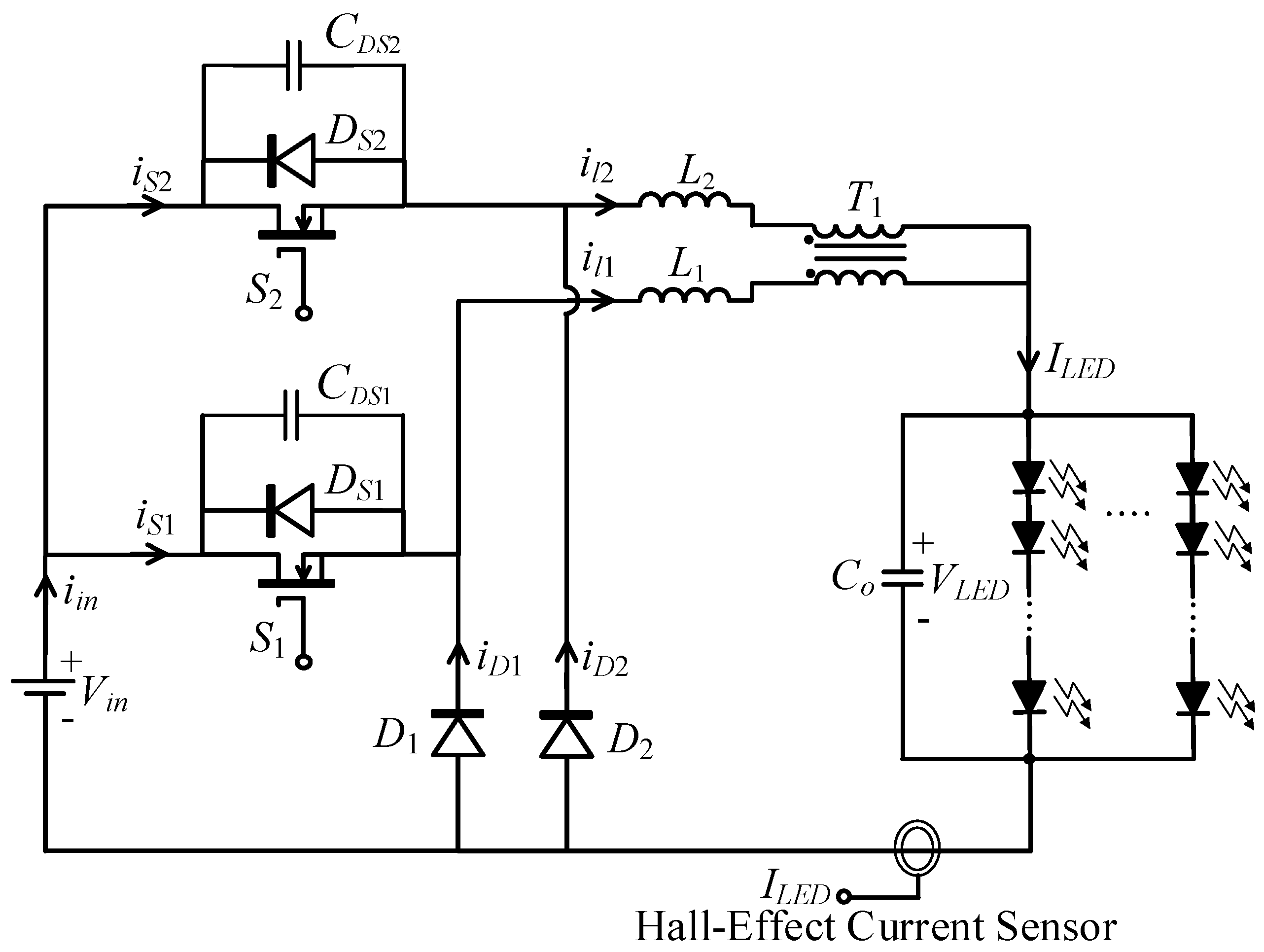
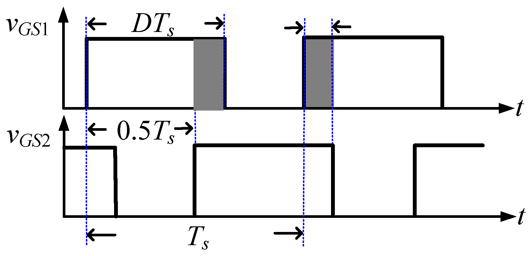
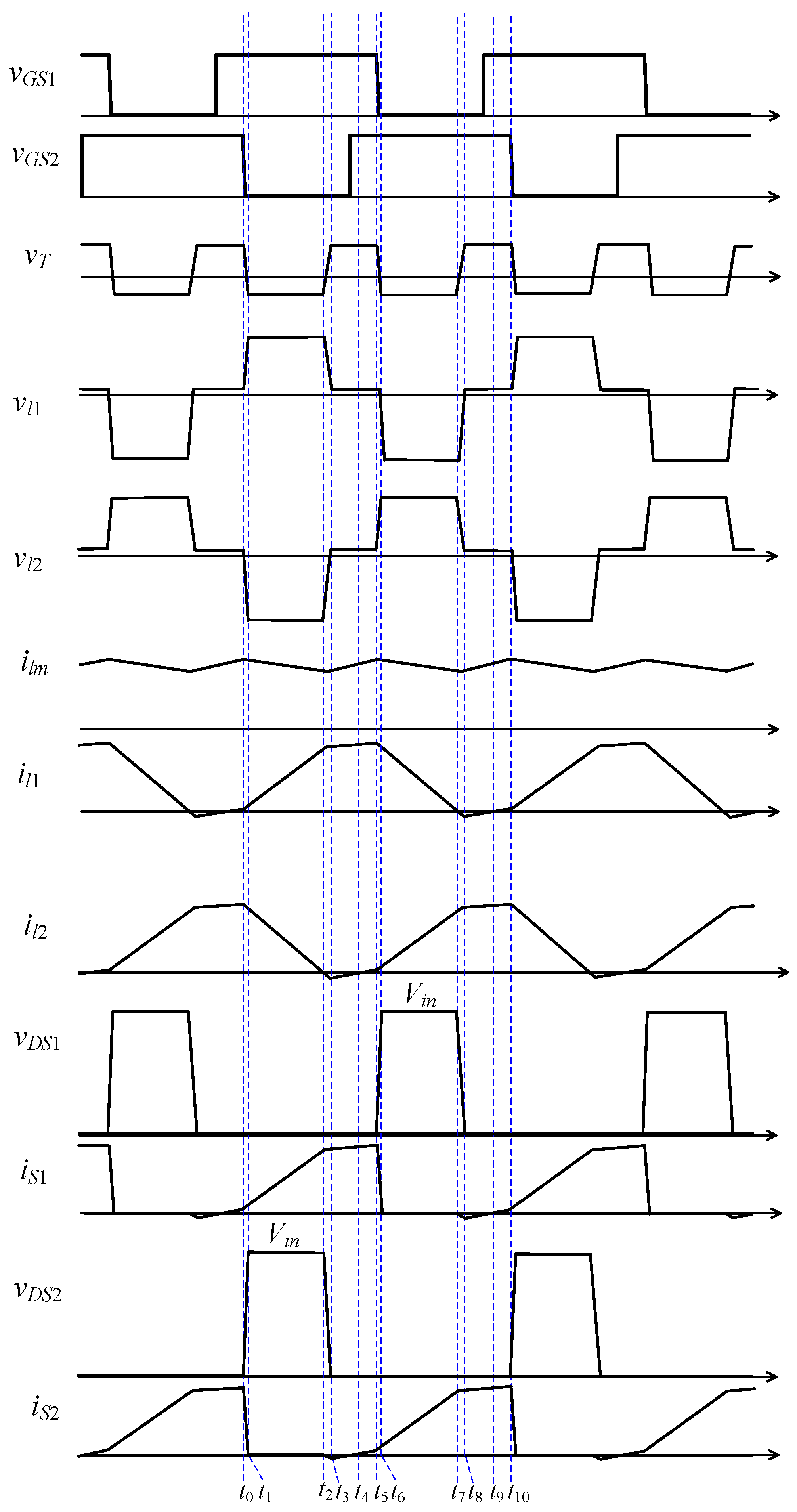
Figure 1 shows the proposed LED driver, which is mainly composed of two buck converters. One buck converter consists of a MOSFET S1, a freewheel diode D1, an inductor L1, and one winding of a coupled inductor T1, while the other converter consists of a MOSFET S2, a freewheel diode D2, an inductor L2, and the other winding of the coupled inductor. Here, the two windings are called primary and secondary windings. Capacitances CDS1 and CDS2 and diodes DS1 and DS2 are the parasitic capacitances and intrinsic diodes of S1 and S2. S1 and S2 are alternately turned on and off by two gated voltages, vGS1 and vGS2. As shown in Figure 2, vGS1 and vGS2 are high-frequency square waveforms. They have the same frequency fs and the same duty cycle D, and there is an overlap time during which both square waves are high voltage.
The coupled inductor consists of a magnetic core and two windings with the same number of turns. It is modeled by using a simplified transformer model, as shown in Figure 3, where L11 and L22 represent the leakage inductance of each winding, Tc is an ideal transformer with a turn ratio equal to 1:1, and magnetizing inductance is LM. The voltage across LM, the current flowing in the two windings, and the magnetizing inductance are denoted as , , , and , respectively. Based on the simplified model, the relation between these currents can be expressed as:
Adding (1) and (2), we obtain:
Equation (3) states that magnetizing current is equal to the sum of the two winding currents, i.e., if the magnetizing current remains constant, the magnetizing current can be converted to flow between the two windings. Using (3) and Faraday’s law of inductance, the following equation is written:
2.2. Steady-State Circuit Analysis
2.2.1. Equivalent Circuits of Different Operating Modes
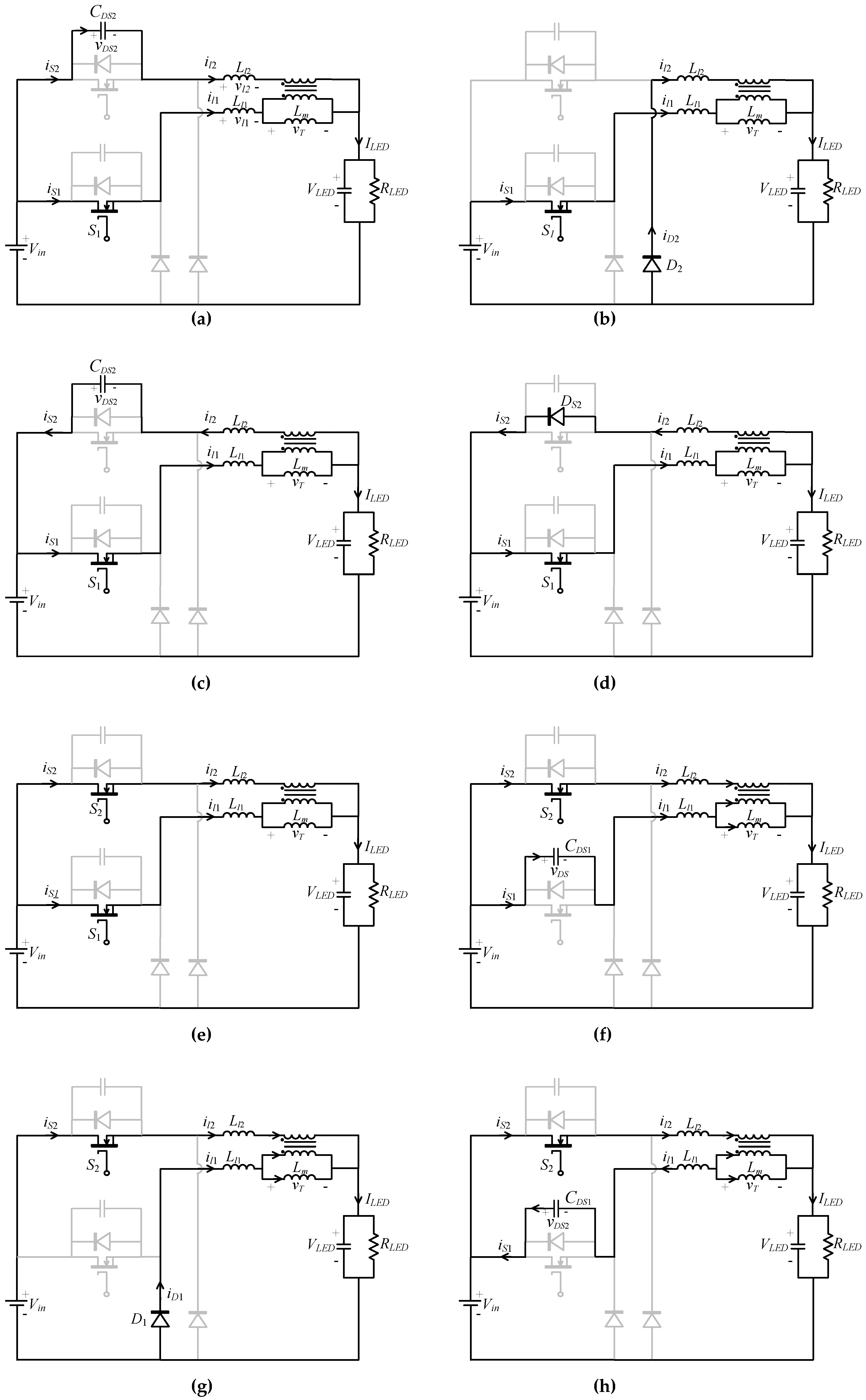
In order to ensure ZVS and ZCS operation, buck converters are designed to operate in DCM. At steady-state operation, the circuit operation can be divided into ten operating modes in one high-frequency cycle. Figure 4 shows the equivalent circuits for different operating modes, where the leakage inductance L11 and L22 are combined with L1 and L2:
As shown in Figure 4a, the voltages across Ll1 and Ll2 are denoted as and , respectively. The following assumptions are made for simplifying the circuit analysis:
- The resistances of all components are neglected.
- Ll1 and Ll2 are equal (Ll1 = Ll2 = Ll).
- LM is large; hence, only changes slightly within one switching period.
- The output capacitance Co is large enough to have a constant output voltage .
The conceptual voltage and current waveforms of the main components for each operation mode are shown in Figure 5.
2.2.2. Detailed Circuit Analysis of Different Operating Modes
Mode I (t0 < t < t1)
Before mode I, S1 and S2 are both on, as shown in Figure 4j. Because S2 is turned on before S1, most of flows through the secondary winding. Therefore, is much larger than . Mode I starts at the moment when S2 is turned off. Figure 4a shows the equivalent circuit. S1 remains on, and charges the parasitic capacitance CDS2. Because CDS2 is very small and is high, CDS2 is quickly charged to Vin. When is equal to Vin, mode I ends. As mentioned above, because CDS2 is small and the charging current is large, the duration of this mode is very short.
Mode II (t1 < t < t2)
S2 is off, and the voltage is maintained at . The current converts from S2 to flow through D2 to the output terminal. From Figure 4b, the voltage equations of the buck converters are as follows:
Adding (7) and (8) results in:
Applying Faraday’s law to Ll1 and Ll2 and using (3) results in:
Substituting (4) and (10) into (9) yields:
Substituting (11) into (7) and (8) yields:
Because LM is much larger than Ll, (12) and (13) show that is positive and is negative. Therefore, rises and decreases. In other words, when S2 is turned off, the current flowing through the secondary winding of the coupled inductor is converted to flow through the primary winding. When the current drops to zero, the circuit enters the next operating mode.
Mode III (t2 < t < t3)
This mode describes the short duration of discharging CDS2 to −0.7 V. From Figure 4c, the voltages across Ll1 and Ll2 are:
Adding (14) and (15) yields:
Substituting (4) and (10) into (16) derives:
Substituting (17) into (14) and (15) yields:
At the beginning of this mode, is equal to Vin. Equation (19) reveals that is negative. Therefore, continues to decrease from zero to become negative. The capacitance is discharged, and decreases. From (17) to (19), it can be seen that vT and increase, while decreases. As soon as decreases to −0.7 V, DS2 is turned on, and the circuit begins operating in mode IV.
Mode IV (t3 < t < t4)
From Figure 4d, neglecting the diode conducting voltage, the voltage equations of the buck converters are:
Adding (20) and (21), we obtain:
Substituting (4) and (10) into (22) derives:
Substituting (23) into (20) and (21), we obtain:
From (23) and (24), , , and are all positive, so , , and all increase. Because LM is much larger than Ll, (24) shows that and are small, and and slowly rise. Before rises to zero, changes from low to high level in this mode. When rises to zero and changes its polarity, it flows through S2, and the circuit enters the next operating mode.
Mode V (t4 < t < t5)
S1 and S2 are both on. Before S2 is turned on, DS2 is on to clamp S2 at zero volts, so S2 fulfills ZVS. Figure 4e shows the equivalent circuit of this mode. The equations of , , and are the same as those of mode IV, so , , and continue to rise. When changes from high to low level, S1 is turned off and the circuit enters operation mode VI.
Mode VI (t5 < t < t6) to Mode X (t9 < t < t10)
Figure 4f–j represents the equivalent circuits of operating modes VI to X, respectively. The circuit operation of modes VI to X is similar to that of modes I to V so is not be repeated here.
When changes from high to low level, S2 is turned off, and the circuit enters mode I of the next high-frequency cycle.
3. Mathematical Equation Derivation
3.1. Magnetizing Current and Inductance Design Equation
According to the previous assumption that LM is large enough, the magnetizing current ILM can be regarded as a constant. In addition, LM is assumed to be much higher than Ll. Therefore, in mode II, from (12) and (13), and are approximately equal to:
Mode III describes the process in which the parasitic capacitance of S2 is discharged from Vin to −0.7 V. In general, CDS2 is small, so the duration of mode III is very short. During this brief period, the drop of is also very small, so when mode III ends, is almost equal to zero (as shown in Figure 5).
In modes IV and V, from (24), vl1 and vl2 are approximately equal to zero:
Because and are almost zero, and hardly change during modes IV and V. To summarize the above description, in mode II, the increasing value of is equal to the decreasing value of , and the increasing value (or decreasing value) is approximately equal to ILM, which can be expressed as:
where represents the duration of mode II ( = − )
In mode II, is negative and decreases. On the contrary, in modes IV and V, is positive and increases. The sum of the durations of modes IV and V is defined as tr (tr = t5 − t3). At a steady-state operation, the average voltage of is equal to zero. Using (11) and (23) yields:
The sum of the fall time and rise time of equals half of the switching period:
where Ts is the switching period of the active switch. Substituting (30) into (29) gives:
Because both tr and tf must be positive values, (30) and (31) imply that the constraints for realizing the LED driver in this study are:
As mentioned above, because the rise amount of il1 in mode II is almost equal to ILM, the following equation can be deduced by substituting (31) into (28):
At steady-state operation, ILM is equal to the LED current:
Using (35), it can be deduced that the inductance of Ll is equal to:
where Po represents the output power of the LED driver.
3.2. LED Voltage Ripple Factor
Figure 6 shows the conceptual waveform of the magnetizing current. Using (23) and (32), the change in is approximately equal to:
The output capacitor is charged when is higher than ILED. The light blue area represents the amount of charge flowing into Co, expressed as:
Using (38), the ripple and ripple factor of the output voltage are expressed as:
4. Prototype LED Driver and Experimental Results
4.1. Parameter Design and Control Circuit
A 180 W prototype of the proposed LED driver was built and tested to verify its feasibility. The specifications is shown in Table 1. The load consisted of sixty 3 W LEDs, and the rated voltage and current of each LED were 3.6 V and 0.83 A, respectively. The LEDs were connected as follows: 6 strings of LEDs in parallel, with each string containing 10 LEDs in series. Hence, the output voltage and current at the rated power operation were 36 V and 5.0 A, respectively. The LED equivalent resistance RLED was calculated to be 7.2 Ω. In this illustrative example, the ripple factor of output voltage was designed to be less than 1%.
Using (36), the values of Ll1 and Ll2 were obtained:
For a buck converter operating in DCM, the input power is inversely proportional to the inductance value. Here, assuming 95% energy conversion efficiency, Ll1 and Ll2 were designed to be 45.6 μF. As mentioned earlier in this article, the magnetizing inductance should be much higher than the value of Ll1 and Ll2. Here, the magnetizing inductance was 732 μF, which was about 16 times that of Ll1 and Ll2.
Using (40), the value of Co was calculated at a 1% ripple factor:
In order to have a ripple factor of less than 1%, a metal-film capacitor with capacitance of 1 μF was chosen. The component parameters are listed in Table 2.
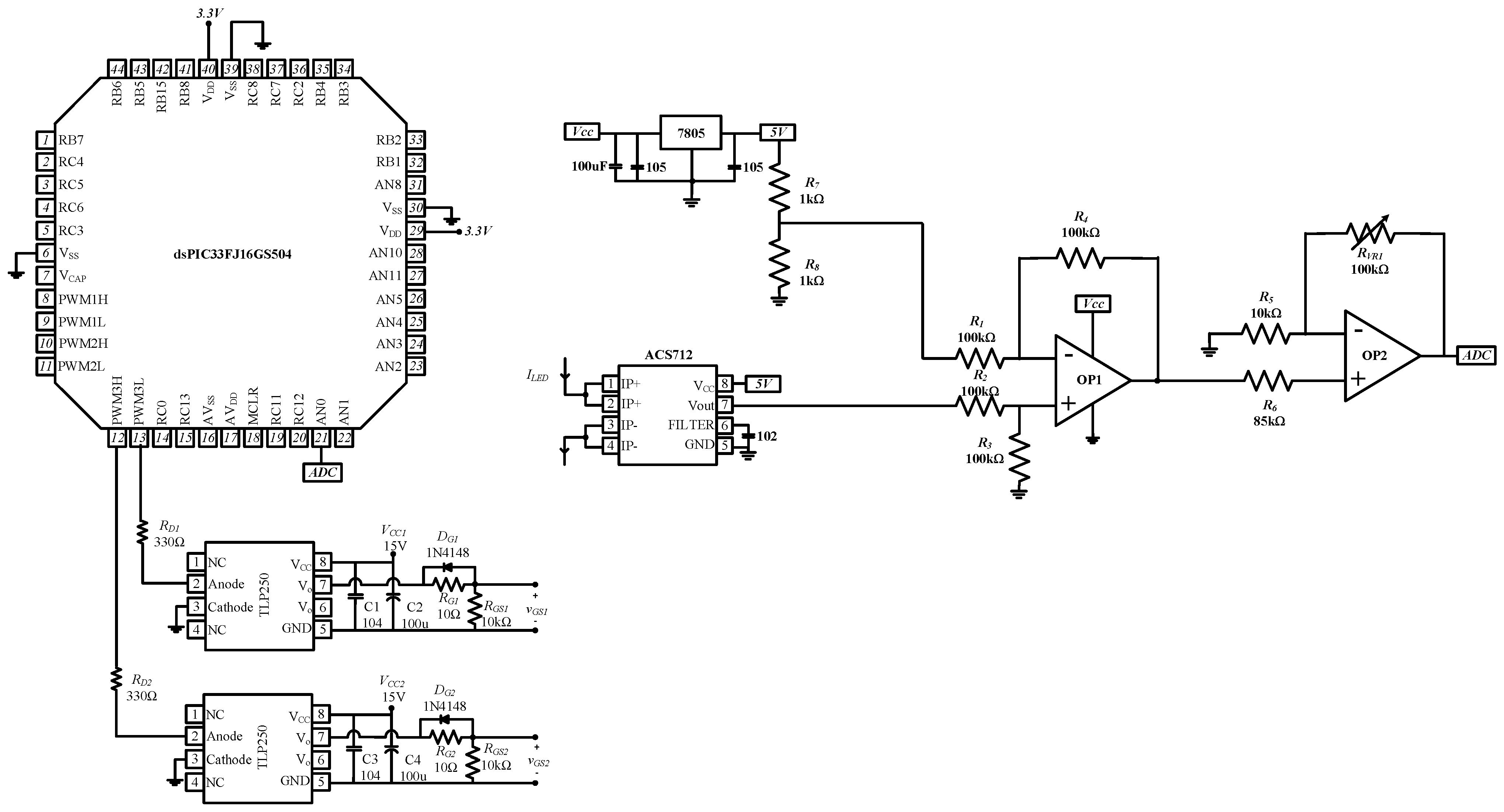
As shown in (36), the output power is inversely proportional to the switching frequency. Therefore, the LED current can be regulated by a frequency control scheme. The control circuit is shown in Figure 7. The output voltages of the microcontroller (dsPIC33FJ16GS504) were fed to two gate drivers (TLP250) that output vGS1 and vGS2 to alternately turn S1 and S2 on and off. The current sensor (ACS712) sensed the LED current and output a voltage value proportional to the magnitude of the current. The difference between the output voltage of the current sensor and a reference value was measured by the operational amplifier (OP1) and sent to the other operational amplifier (OP2) for voltage amplification; then, the amplified voltage was sent to the microprocessor to adjust the switching frequency.
4.2. Experimental Results
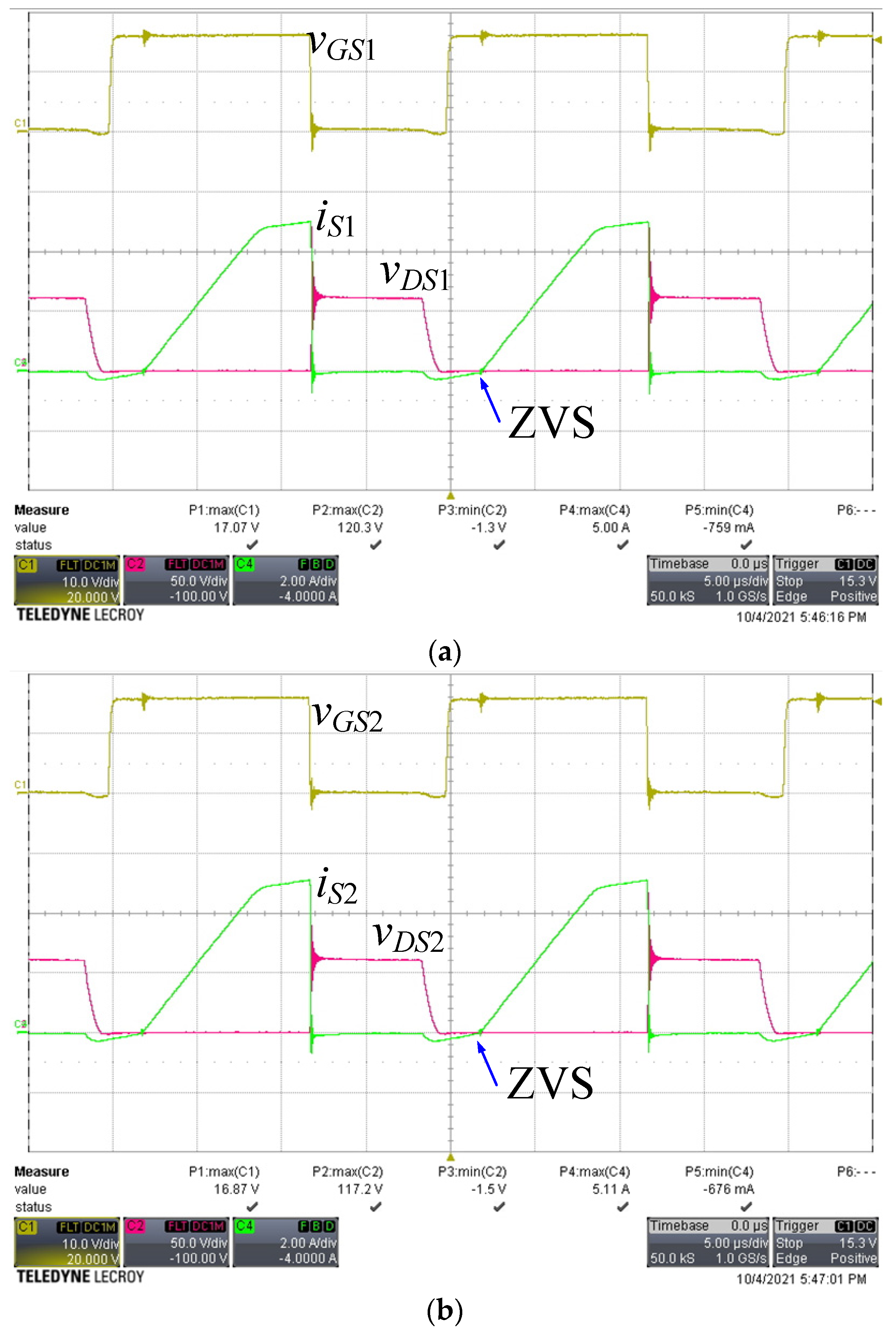
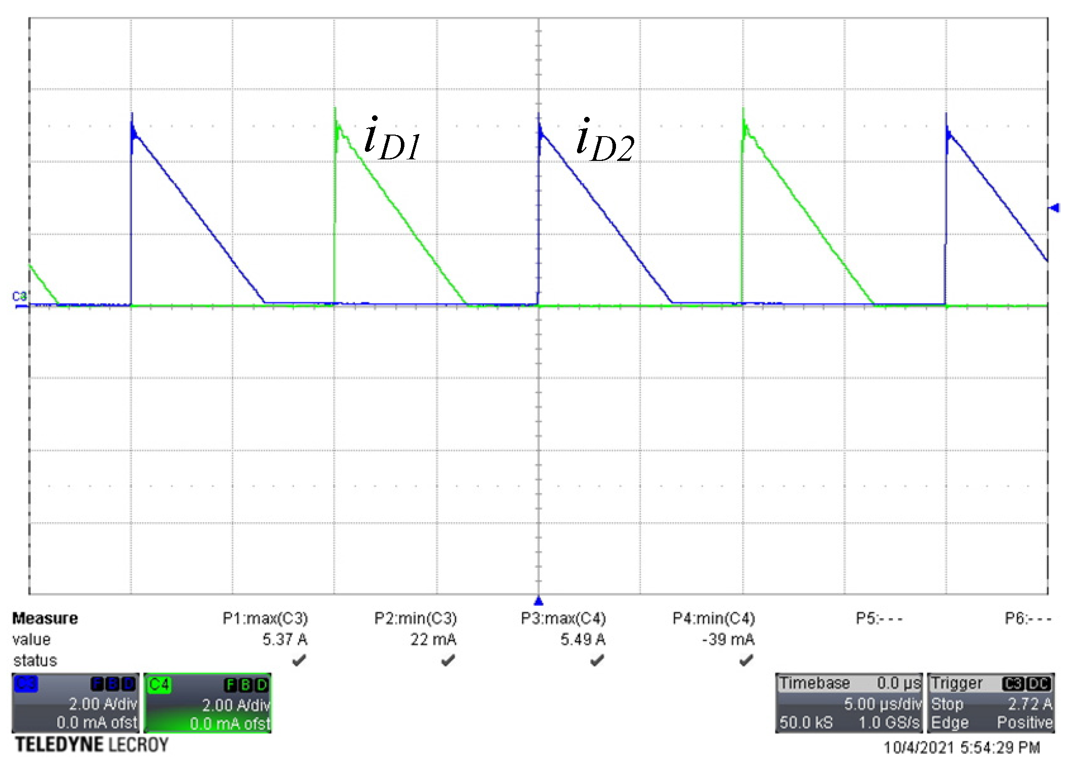
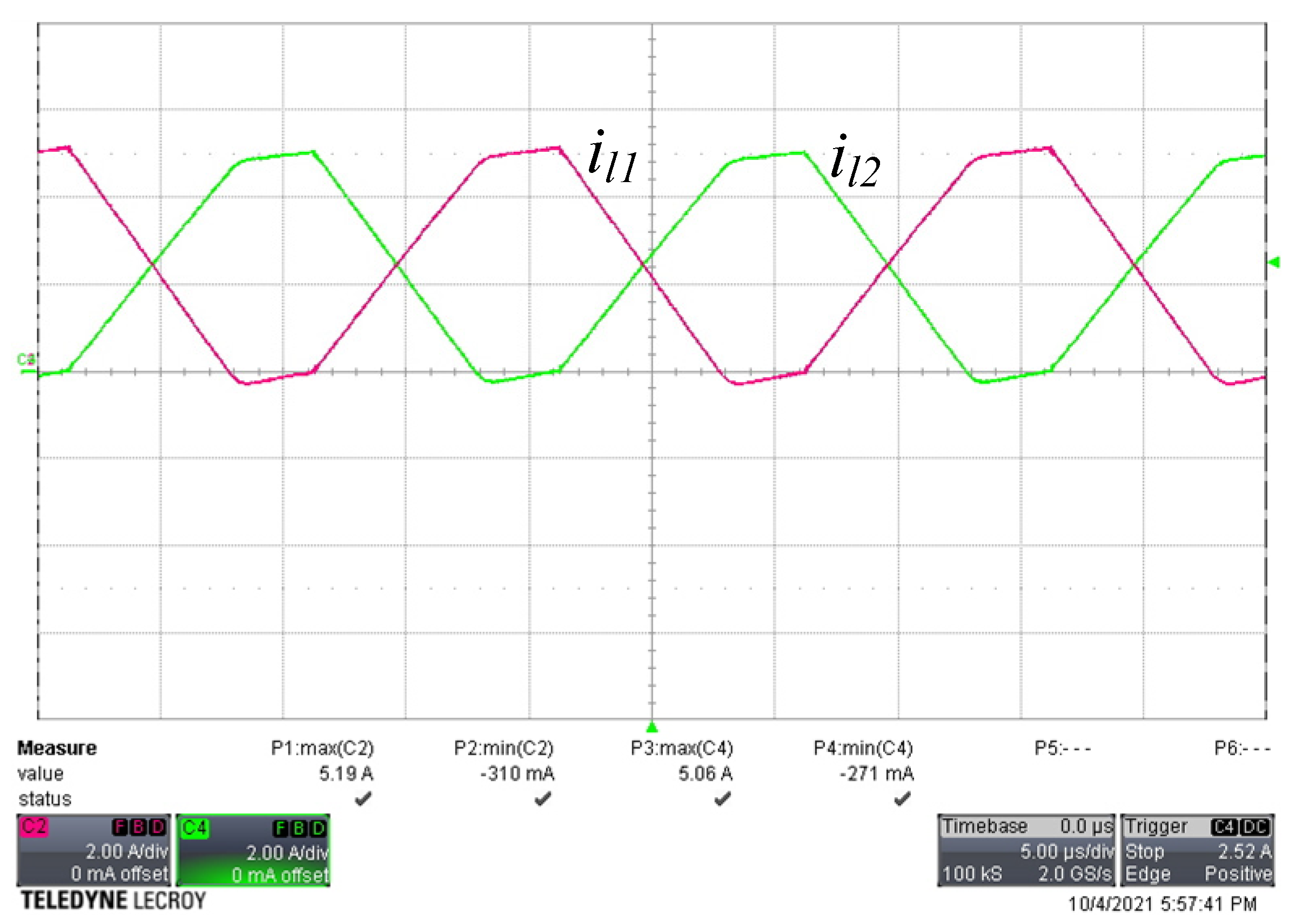
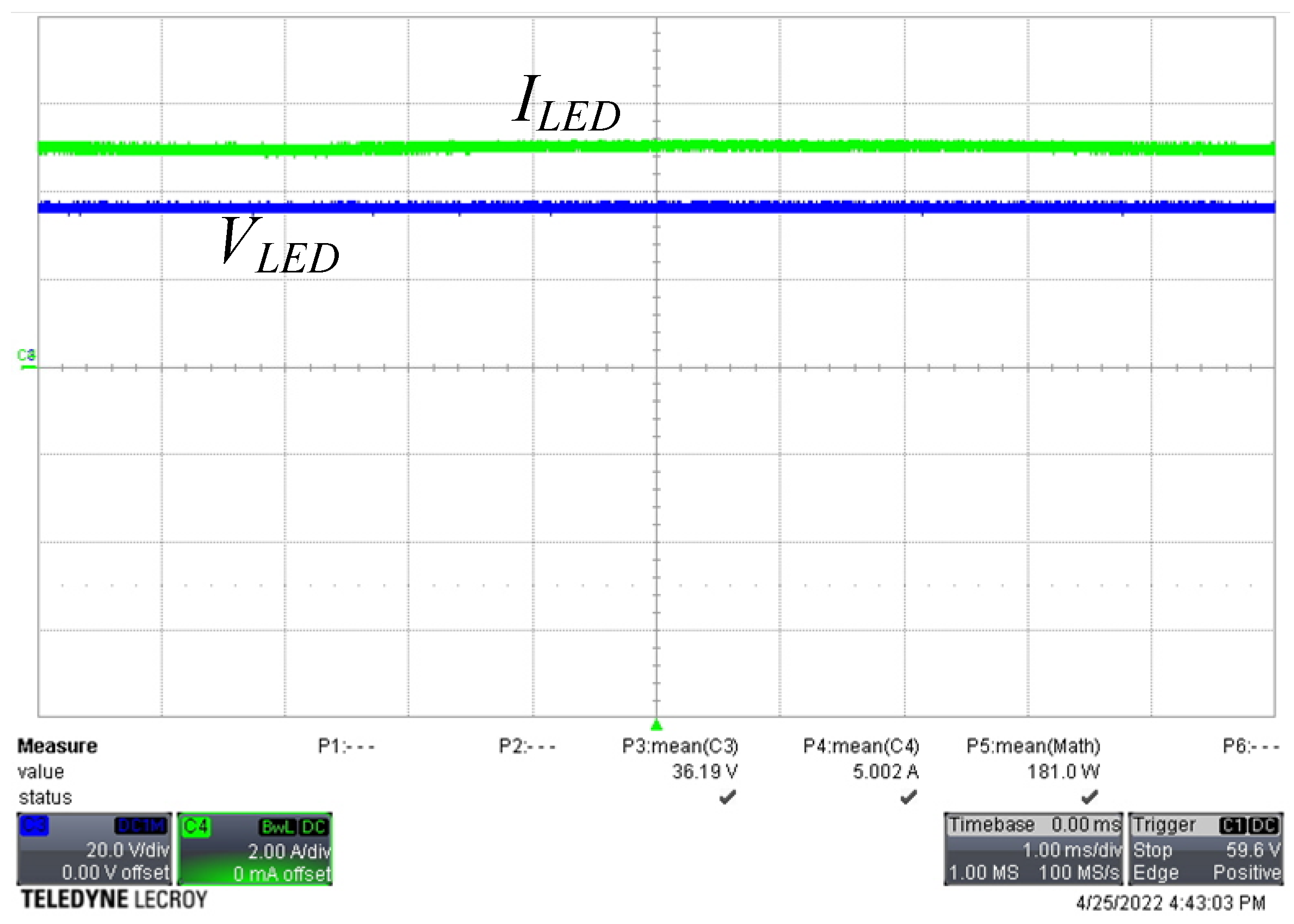
Figure 8 shows the voltage and current waveforms of the two active switches. There was a small amount of negative current flowing through each active switch, and the gate voltage changed from low to high before the negative current became positive. When the negative current discharged the parasitic capacitance of the switch to −0.7 V, it turned on the intrinsic diode. Because the intrinsic diode was turned on, the voltage across the switch was clamped to almost zero voltage; therefore, the switch satisfied ZVS operation. Figure 9 shows the current waveforms of the freewheel diodes. Both diode currents dropped to zero and naturally turned off, leading to ZCS operation. Figure 10 shows the waveforms of the current in both windings of the coupled inductor. As predicted, the magnetizing current was converted between the two windings, and both winding currents dropped to slightly below zero. Figure 11 shows the output voltage and output current waveforms. The measured output power was equal to 181.2 W. The calculated ripple factor was 0.8%. The power losses in the components at the rated power operation were measured and are shown in Table 3. Due to ZVS and ZCS operation, the circuit efficiency was as high as 97.5%.
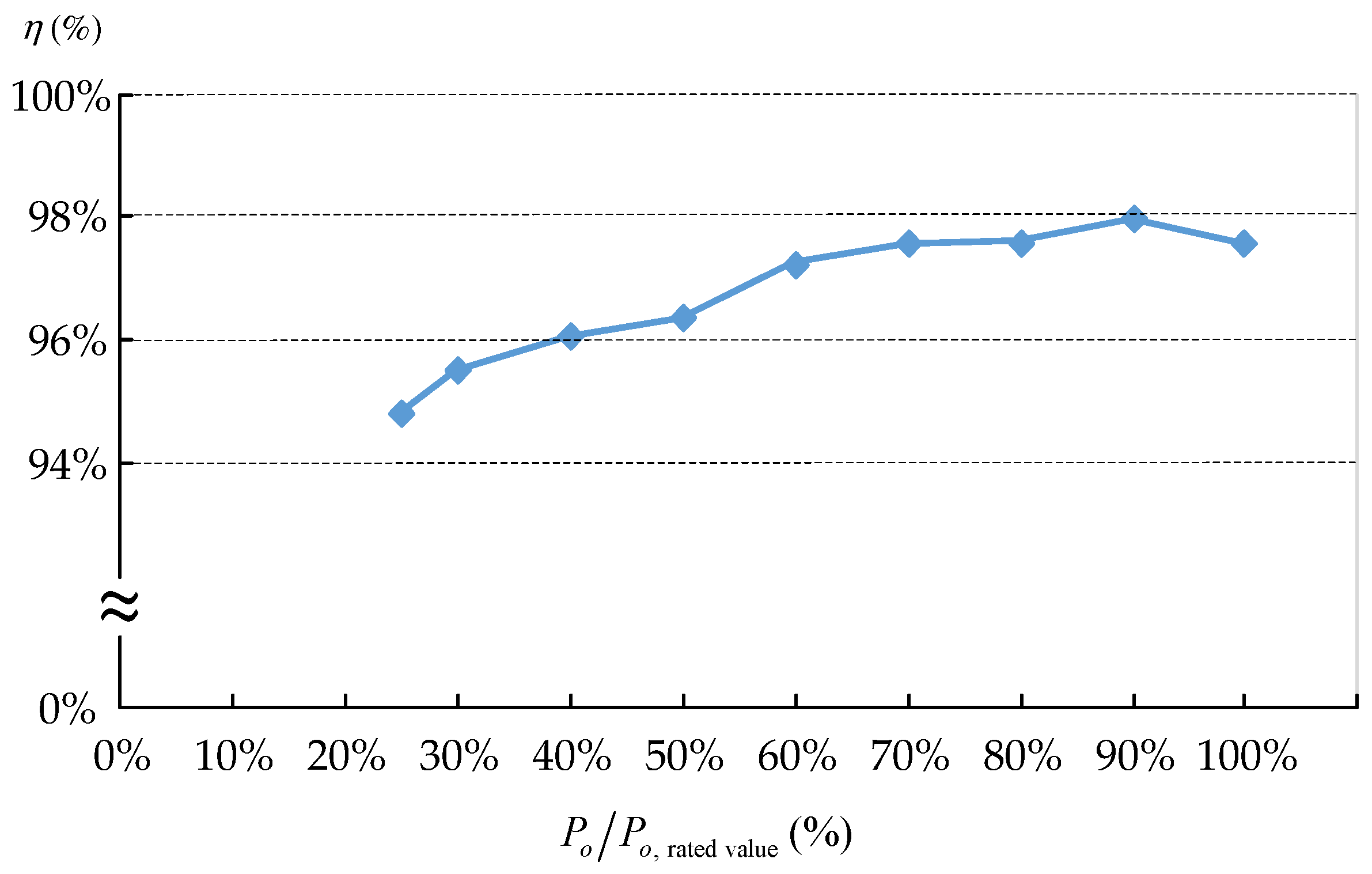
The LED power was controlled by adjusting the switching frequency. The measured efficiency curves over a load range of 25% to 100% rated power are shown in Figure 12. Efficiency slightly dropped when the LEDs were dimmed from 80% to 25% of the rated power.
5. Conclusions
In this study, an interleaved DC-DC converter was designed for driving high-power LEDs. The circuit topology consists of two buck converters, which are alternately turned on and off. A coupled inductor consisting of a magnetic core and two windings is shared by the two buck converters. To maintain the magnetic flux continuity, the magnetizing current is converted between the two windings. In this way, the freewheel diodes can operate at ZCS and the active switches can operate at ZVS. In addition, because the magnetizing current is nearly constant and the buck converter continuously supplies the magnetizing current to the output terminal, the ripple voltage remains very small even when a small metal-film capacitor is used.
Detailed steady-state operation was analyzed and the mathematical equations for different modes were derived; thereafter, the component parameters were designed. Finally, a 180 W prototype circuit was implemented to drive sixty 3 W LEDs. By adjusting the switching frequency of the active switches, the LED power was dimmed from 100% to 25% rated power. Owing to ZVS and ZCS operation, the switching losses of the semiconductor devices were effectively reduced, leading to a high circuit efficiency. The measured circuit efficiency was as high as 97.5% at the rated power operation. At a low power operation, the circuit efficiency remained high. When the circuit was operated at 25% of its rated power, the efficiency was 94.7%. The output capacitor was a 1 μF metal-film capacitor; the measured ripple factor of the output voltage was as low as 0.8%. Without the use of any bulk electrolytic capacitors, the long lifetime of the proposed LED driver can be ensured. The experimental results verified the feasibility of the proposed circuit.
Author Contributions
H.-L.C. and L.-C.H. conceived and designed the circuit and analyzed the operating modes; H.H.C. performed circuit simulations and wrote the manuscript; Q.-Y.W. carried out the prototype LED driver and both measured and analyzed experimental results; C.-A.C. designed parameters of the circuit components and revised the manuscript for submission. All authors have read and agreed to the published version of the manuscript.
Funding
This research was funded by the Ministry of Science and Technology, R.O.C., under grant MOST 110-2221-E-214-015.
Conflicts of Interest
The authors declare no conflict of interest.
References
- Zhan, X.; Chung, H.; Zhang, R. Investigation into the use of single inductor for driving multiple series-connected LED channels. IEEE Trans. Power Electron. 2017, 32, 3034–3050. [Google Scholar] [CrossRef]
- Cheng, H.L.; Chang, Y.N.; Yen, H.C.; Hua, C.C.; Su, P.S. An interleaved flyback-typed LED driver with ZVS and energy recovery of leakage inductance. IEEE Trans. Power Electron. 2019, 34, 4497–4508. [Google Scholar] [CrossRef]
- Abdelmessih, G.Z.; Alonso, J.M.; Dalla Costa, M.A. Analysis, design, and experimentation of the active hybrid-series-parallel PWM dimming scheme for high-efficient off-line LED drivers. IET Power Electron. 2019, 12, 1697–1705. [Google Scholar] [CrossRef]
- Sangrody, R.; Pouresmaeil, M.; Marzband, M.; Pouresmaeil, E. Resonance-based optimized buck LED driver using unequal turn ratio coupled inductance. IEEE Trans. Power Electron. 2020, 35, 13068–13076. [Google Scholar] [CrossRef]
- Qiu, Y.; Wang, L.; Wang, H.; Liu, Y.F.; Sen, P.C. Bipolar ripple cancellation method to achieve single-stage electrolytic-capacitor-less High-Power LED driver. IEEE J. Emerg. Sel. Top. Power Electron. 2015, 3, 698–712. [Google Scholar]
- Li, L.; Gao, Y.; Jiang, H.; Mok, P.K.T.; Lau, K.M. An auto-zero-voltage-switching quasi-resonant LED driver with GaN FETs and fully integrated LED shunt protectors. IEEE J. Solid-State Circuits 2018, 53, 913–923. [Google Scholar] [CrossRef]
- Cao, L.; Zhu, Y.; Wu, H. A new electrolytic-capacitor-less LED driver with coupled-inductor. In Proceedings of the 2020 IEEE Applied Power Electronics Conference and Exposition (APEC), New Orleans, LA, USA, 15–19 March 2020. [Google Scholar]
- Yu, W.; Lai, J.H.; Ma, H.B.; Zheng, C. High-efficiency DC–DC converter with twin bus for dimmable LED ighting. IEEE Trans. Power Electron. 2011, 26, 2095–2100. [Google Scholar] [CrossRef]
- Wang, Q.; Li, T.; He, Q.H. Dimmable and cost-effective DC driving technique for flicker mitigation in LED Lighting. J. Disp. Technol. 2014, 10, 766–774. [Google Scholar] [CrossRef]
- Saxena, A.R.; Kulshreshtha, A. Universal bus front end PFC fourth-order buck converter as LED drivers. In Proceedings of the 2017 IEEE Region 10 Conference, Penang, Malaysia, 5–8 November 2017. [Google Scholar]
- Fang, P.; Sheng, B.; Liu, W.B.; Liu, Y.F.; Sen, P.C. Parallel energy buffering LED driver achieves electrolytic capacitor-less and flicker-free operation. In Proceedings of the IEEE Energy Conversion Congress and Exposition, Portland, OR, USA, 23–27 September 2018. [Google Scholar]
- Sebastian, J.; Villegas, P.J.; Nuno, F.; Hernando, M.M. High-efficiency and wide-bandwidth performance obtainable from a two-input buck converter. IEEE Trans. Power Electron. 1998, 13, 706–717. [Google Scholar] [CrossRef]
- Zhao, K.; Ciufo, P.; Perera, S. Lifetime analysis of aluminum electrolytic capacitor subject to voltage fluctuations. In Proceedings of the 14th International Conference on Harmonics and Quality of Power, Bergamo, Italy, 26–29 September 2010. [Google Scholar]
- Lee, J.H.; Yu, D.H.; Kim, J.G.; Kim, Y.H.; Shin, S.C.; Jung, D.Y.; Jung, Y.C.; Won, C.Y. Auxiliary switch control of a bidirectional soft-switching dc/dc converter. IEEE Trans. Power Electron. 2013, 28, 5446–5457. [Google Scholar]
- Yun, J.J.; Choe, H.J.; Hwang, Y.H.; Park, Y.K.; Kang, B. Improvement of power-conversion efficiency of a dc-dc boost converter using a passive snubber circuit. IEEE Trans. Ind. Electron. 2012, 59, 1808–1814. [Google Scholar] [CrossRef]
- Moo, C.S.; Chen, Y.J.; Cheng, H.L.; Hsieh, Y.C. Twin-buck converter with zero-voltage transition. IEEE Trans. Ind. Electron. 2011, 58, 2366–2371. [Google Scholar] [CrossRef]
- Yu, X.; Su, J.; Guo, S.; Zhong, S.; Shi, Y.; Lai, J. Properties and synthesis of lossless snubbers and passive soft-switching PWM converters. IEEE Trans. Power Electron. 2020, 35, 3807–3826. [Google Scholar] [CrossRef]
- Yang, J.W.; Do, H.L. Soft-switching bidirectional DC-DC converter using a lossless active snubber. IEEE Trans. Power Electron. 2014, 61, 588–1596. [Google Scholar] [CrossRef]
- Yang, J.W.; Do, H.L. High-efficiency ZVS AC-DC LED driver using a self-driven synchronous rectifier. IEEE Trans. Circuits Syst. I Regul. Pap. 2014, 61, 2505–2512. [Google Scholar] [CrossRef]
- Marvi, M.; Fotowat-Ahmady, A. A fully ZVS critical conduction mode boost PFC. IEEE Trans. Power Electron. 2012, 27, 1958–1965. [Google Scholar] [CrossRef]
- Huang, B.; Torrico, X.M.; GLiang, Y. High efficiency telecom rectifier designed for wireless communication networks. In Proceedings of the IEEE 33rd International Telecommunications Energy Conference (INTELEC), Amsterdam, The Netherlands, 9–13 October 2011. [Google Scholar]
Figure 1.
Circuit topology of the proposed LED driver.

Figure 2.
High-frequency waveforms of gated voltages vgS1 and vgS2.

Figure 3.
Simplified transformer model of the coupled inductor.

Figure 4.
Equivalent circuits of different operating modes. (a) Mode I; (b) mode II; (c) mode III; (d) mode IV; (e) mode V; (f) mode VI; (g) mode VII; (h) mode VIII; (i) mode IX; (j) mode X.
Figure 4.
Equivalent circuits of different operating modes. (a) Mode I; (b) mode II; (c) mode III; (d) mode IV; (e) mode V; (f) mode VI; (g) mode VII; (h) mode VIII; (i) mode IX; (j) mode X.


Figure 5.
Conceptual waveforms of the main components.

Figure 6.
Conceptual waveform of the magnetizing current.

Figure 7.
Control circuit.

Figure 8.
Voltage and current waveforms of the active switches. (a) vGS1, vDS1, and iS1; (b) vGS2, vDS2, and iS2 (vGS1, vGS2: 10 V/div, vDS1, vDS2: 50 V/div, iS1, iS2: 2 A/div, time: 5 μs/div).
Figure 8.
Voltage and current waveforms of the active switches. (a) vGS1, vDS1, and iS1; (b) vGS2, vDS2, and iS2 (vGS1, vGS2: 10 V/div, vDS1, vDS2: 50 V/div, iS1, iS2: 2 A/div, time: 5 μs/div).

Figure 9.
Current waveforms of the freewheel diodes. (iD1, iD2: 2 A/div, time: 5 µs/div).

Figure 10.
Current waveforms of the winding current of the coupled inductor (il1, il2: 2A/div, time: 5 µs/div).
Figure 10.
Current waveforms of the winding current of the coupled inductor (il1, il2: 2A/div, time: 5 µs/div).

Figure 11.
Waveforms of LED voltage and current (VLED: 20 V/div, ILED: 2 A/div, time: 1 ms/div).

Figure 12.
Measured circuit efficiency at different output power levels.


Table 1.
Specifications of the proposed LED driver.
| Item | Value |
|---|---|
| Input Voltage, Vin | 60 V |
| Output Voltage, VLED | 36 V |
| Output Power, Po | 180 W |
| Voltage Ripple Factor, rv | <1% |
| Switching Frequency, fs (at rated power) | 50 kHz |
| 3 W LED Rated Voltage | 3.6 V |
| 3 W LED Rated Current | 0.83 A |
Table 2.
Component parameters.
| Item | Value |
|---|---|
| Inductance, Ll1, Ll2 | 45.6 μH, 45.6 μH |
| Magnetizing Inductance, LM | 732 μH |
| Output capacitance, Co | 1 μF (metal-film capacitor) |
| Diodes D1, D2 | C3D10060A |
| Active switches S1, S2 | STW52NK25Z |
Table 3.
Measured losses in the components.
| Item | Value |
|---|---|
| Coupled Inductors, LM | 0.8 W |
| Inductors, L1, L2 | 0.23 W, 0.23 W |
| Active Switches, S1, S2 | 0.8 W, 0.8 W |
| Diodes, D1, D2 | 0.7 W, 0.7 W |
| Output Capacitor, Co | 0.3 W |
Publisher’s Note: MDPI stays neutral with regard to jurisdictional claims in published maps and institutional affiliations. |
© 2022 by the authors. Licensee MDPI, Basel, Switzerland. This article is an open access article distributed under the terms and conditions of the Creative Commons Attribution (CC BY) license (https://creativecommons.org/licenses/by/4.0/).
Share and Cite
MDPI and ACS Style
Cheng, H.-L.; Hwang, L.-C.; Chang, H.H.; Wang, Q.-Y.; Cheng, C.-A. High-Efficiency Flicker-Free LED Driver with Soft-Switching Feature. Micromachines 2022, 13, 797. https://0-doi-org.brum.beds.ac.uk/10.3390/mi13050797
AMA Style
Cheng H-L, Hwang L-C, Chang HH, Wang Q-Y, Cheng C-A. High-Efficiency Flicker-Free LED Driver with Soft-Switching Feature. Micromachines. 2022; 13(5):797. https://0-doi-org.brum.beds.ac.uk/10.3390/mi13050797
Chicago/Turabian StyleCheng, Hung-Liang, Lain-Chyr Hwang, Heidi H. Chang, Qi-You Wang, and Chun-An Cheng. 2022. "High-Efficiency Flicker-Free LED Driver with Soft-Switching Feature" Micromachines 13, no. 5: 797. https://0-doi-org.brum.beds.ac.uk/10.3390/mi13050797
Note that from the first issue of 2016, this journal uses article numbers instead of page numbers. See further details here.