3D NAND Flash Based on Planar Cells

Macronix, Via Val Passiria 8, Milan 20100, Italy
Computers 2017, 6(4), 28; https://0-doi-org.brum.beds.ac.uk/10.3390/computers6040028
Submission received: 28 July 2017
/
Revised: 17 September 2017
/
Accepted: 27 September 2017
/
Published: 24 October 2017
(This article belongs to the Special Issue 3D Flash Memories)
Abstract
:In this article, the transition from 2D NAND to 3D NAND is first addressed, and the various 3D NAND architectures are compared. The article carries out a comparison of 3D NAND architectures that are based on a “punch-and-plug” process—with gate-all-around (GAA) cell devices—against architectures that are based on planar cell devices. The differences and similarities between the two classes of architectures are highlighted. The differences between architectures using floating-gate (FG) and charge-trap (CT) devices are also considered. Although the current production of 3D NAND is based on GAA cell devices, it is suggested that architectures with planar cell devices could also be viable for mass production.
1. Introduction
It is commonly understood that there is a lesser-known observation of Gordon Moore, sometimes referred as Moore’s second law, which is related to the cost expenditure increase to produce the next generation of processors. Whether we want to refer to Moore or not, fab cost and yield are economic limitation factors for the increase in the number of transistors per chip per each new generation. Nevertheless, we cannot think of a future without more powerful computers and huge data saved in the cloud; therefore the race keeps going. Regarding data, the industry is forced to explore new ways to pack bits in a smaller space, while the physical limitations on further miniaturization block the old path.
NAND flash production is transitioning from 2D to 3D by expanding in the third dimension rather than shrinking, thus relaxing the optical lithography needs. However, significant investments are still required to accompany this transition in the manufacturing sites: yield issues have to be addressed and manufacturing costs are limiting the economic viability of the solutions.
The cost advantage of 3D NAND therefore needs to be proven by manufacturing a significant and sufficient number of layers with proper yield.
The structure of the NAND flash cell and the NAND flash string has changed significantly with respect to traditional 2D NAND. Today, there are still several different approaches pursued by NAND manufacturers; the differences in some cases are very substantial, and new types of challenges arise from new architectures. Even if these are studied for several years, they must be proven in volume production.
In this article, we review the most popular 3D structures pursued by manufacturers and highlight the diversities and similarities among the various approaches. We note that the most common structure of the flash cell in 3D NAND today is a gate-all-around (GAA) cell made by a generic “punch-and-plug” process, but that structures with planar cells have also been demonstrated to be viable.
2. Transition to 3D NAND
The basic idea behind 3D NAND is to “grow” cells in the vertical dimension, thus reaching a higher density per area. The necessity stems from the fact that 2D NAND has reached lithographic limitations and no further shrinks are possible. Differently to building a house, where each floor must be grown one on top of the other by repeating construction steps, recent 3D NAND approaches are leveraging on process schemes that use common processing steps to define the geometries of all the cells of the vertical stack at once. This approach is necessary to retain the minimum number of processing steps and thermal reflows. In a first approximation, the number of processing steps is not proportional to the number of layers, as it would be in the case of merely repeating the formation of the 2D strings one on top of the other.
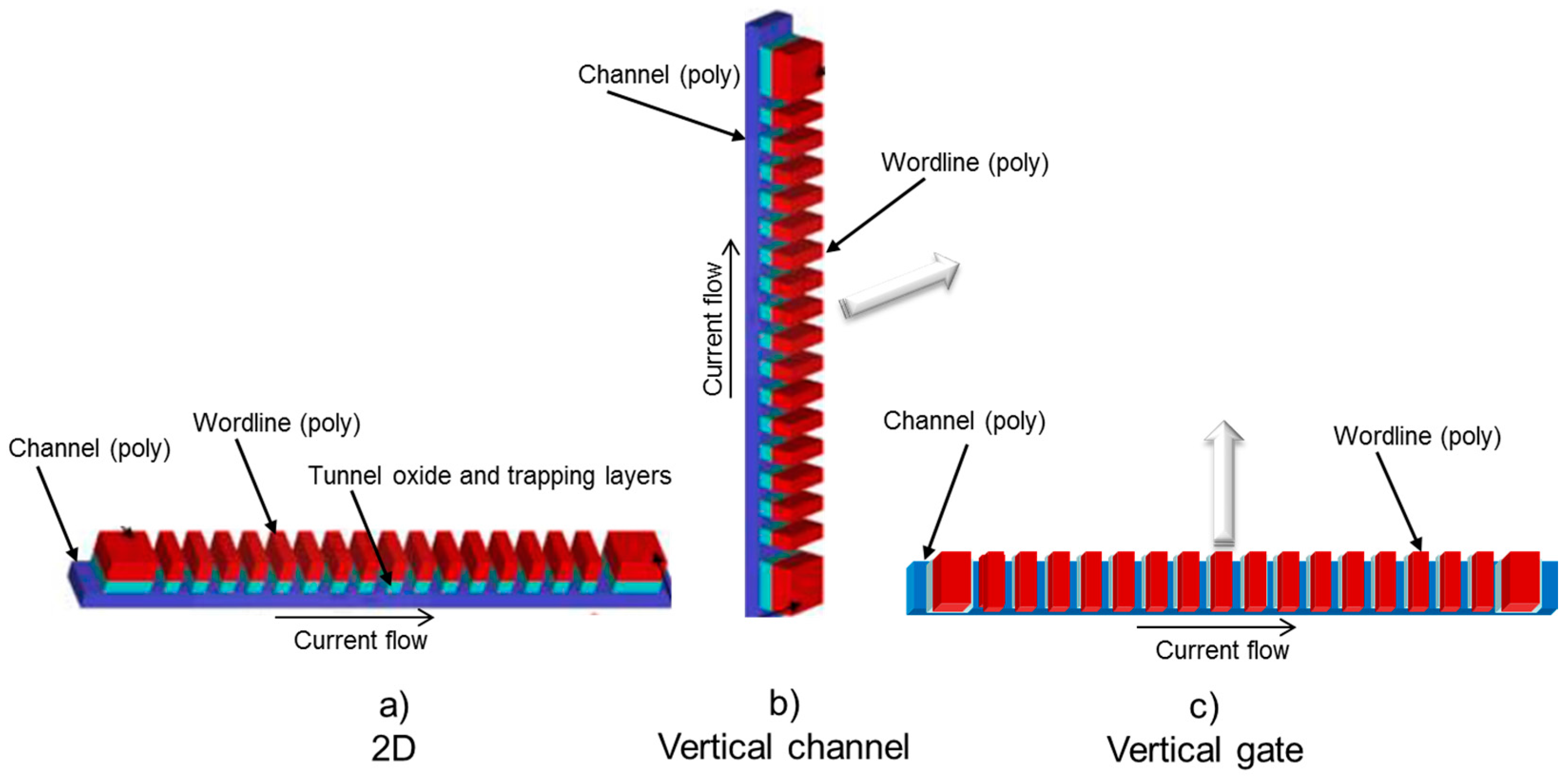
Conceptually, a modern 3D NAND structure could be conceived by starting from the 2D NAND string building block (Figure 1a). By turning the 2D NAND string upside, the resulting 3D structure has a vertical channel. Another way to imagine the 3D NAND consists of rotating the 2D NAND string on its side (Figure 1c); the channel becomes horizontal and the gates run vertically (the structure is replicated vertically so as to obtain multiple horizontal NAND strings). In both cases, we can observe that there is an alternation of polysilicon layers and oxide layers in the vertical direction; in the example of Figure 1b, the wordlines are stacked vertically (with oxide in between), and in the example of Figure 1c, the polysilicon channel is stacked vertically with oxide in between. Starting from this simple consideration, we can derive the basic process flow of forming a 3D NAND. A polysilicon/oxide layer stack is first grown and then the stack is properly etched in order to form the geometries at once. Subsequently, the cells can be formed by deposition of layers on the sidewalls of the etched areas. For the example, the tunnel oxide and polysilicon channel is deposited in the vertical channel structure (Figure 1b), and similarly the tunnel oxide and vertical wordline polysilicon is deposited to form the cells in the vertical gate structure (Figure 1c).
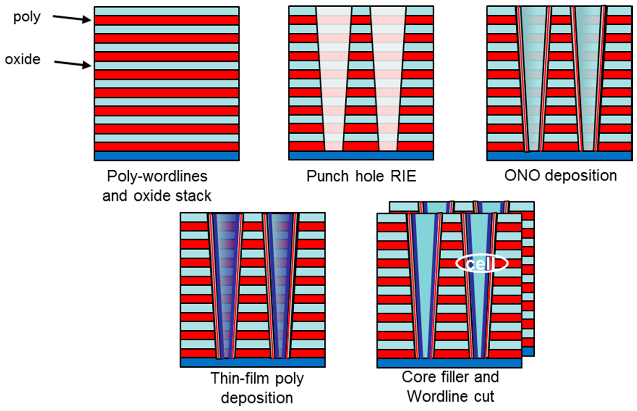
In the rest of this paragraph, the focus is on a simplified process description of two architectures: one vertical channel and one vertical gate. The scope is to highlight some key aspects of the 3D NAND process and architectures. It is worth noting here that a common approach to form the cell stack of vertical channel 3D NAND is by etching holes through the poly/oxide stack followed by deposition of the oxides and channel (punch-and-plug approach). The resulting flash cell device is often referred to as a gate-all-around (GAA) cell [1], because the vertical device has a circular channel (the plug) formed inside a drilled hole and the gate surrounds the channel (all around). This approach is somewhat different from that envisaged in Figure 1b, which results in a planar cell; however, the starting point from a poly/oxide layer stack is the same. The punch-and-plug method was one of the first to be proposed, even if the cell structure is different from the 2D, and it will be used for the example of a vertical channel 3D NAND.
The basic fabrication (Figure 2) of a “gate-first” GAA vertical channel (“gate-last” GAA Vertical Channel methods are a little more complicated) begins with drilling down through the poly/oxide stack by reactive ion etching (RIE) and forming cylindrical holes; then, the tunneling and trapping layers are deposited along the sidewalls of the trenches. Finally, the thin polysilicon channel is deposited, followed by a core filler to form a hollow structure. In bottom source architectures (just as in this example), it is necessary to remove the oxide from the bottom and open the contact to the source line. This operation is critical for the integrity of the oxide and requires special processing steps [2]. In the resulting structure, the single cell transistor is formed in the intersection between the channel and the polysilicon layer (gate). The last necessary step is to form the wordline cut, to separate the NAND pages. It can be noted that the NAND string is vertical, and the string current flows in the vertical direction and is collected by a drain contacting the top of the cell stack. The source current must be provided by source diffusion at the bottom.
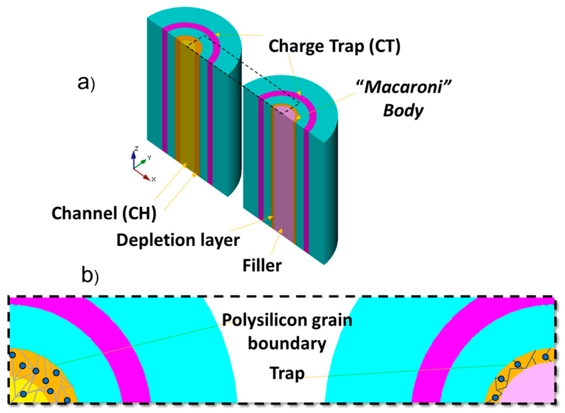
In GAA structures, it is necessary that the drilled hole is relatively large (about 0.12 um), and this is a limitation for shrinking the structure in 2D. In order to avoid degradation and uncontrollability of the Thin Film Transistor (TFT) cell in the subthreshold region due to the polysilicon grain boundary, the adoption of a thin film device is mandatory; the hole is not completely filled—a thin film is deposited and then the remaining space is filled with a dielectric. The cell structure is named “macaroni-type”, and it is shown in Figure 3. Thus, the polysilicon body is made thinner than the depletion width (Figure 3b) to reduce the number of traps and to make subthreshold characteristics of the TFT less dependent on grain boundary traps [1,3].
The transistor cell structure is totally different from the planar cell: the gate is circular and surrounds the channel, as shown in Figure 3.
In a GAA cell, the curvature of the device geometry concentrates the electric field moving toward the center of the structure (the tunnel oxide) creating a field-enhancement (FE) effect. This effect is useful to enhance the programming and erasing operations and to limit the required voltage. However, FE also affects read-disturb (or program-disturb) issues, because the electric field generated by the pass voltages is also enhanced, thus inducing a soft program. In addition, the variations of geometry with the stack height also make the cells along the stack behave differently. Any local variation of the curvature of the cell structure may enhance the negative effects of an increased electric field, and this has also to be considered carefully. Therefore, in GAA cells, special attention must be paid to the design of the programming algorithms for reliable NAND operation [5].
A GAA cell it is not the only option to build vertical channel 3D NAND. For example, in Section 5.3, the single-gate vertical channel (SGVC) is discussed. SGVC concept is similar to that shown in Figure 1b.
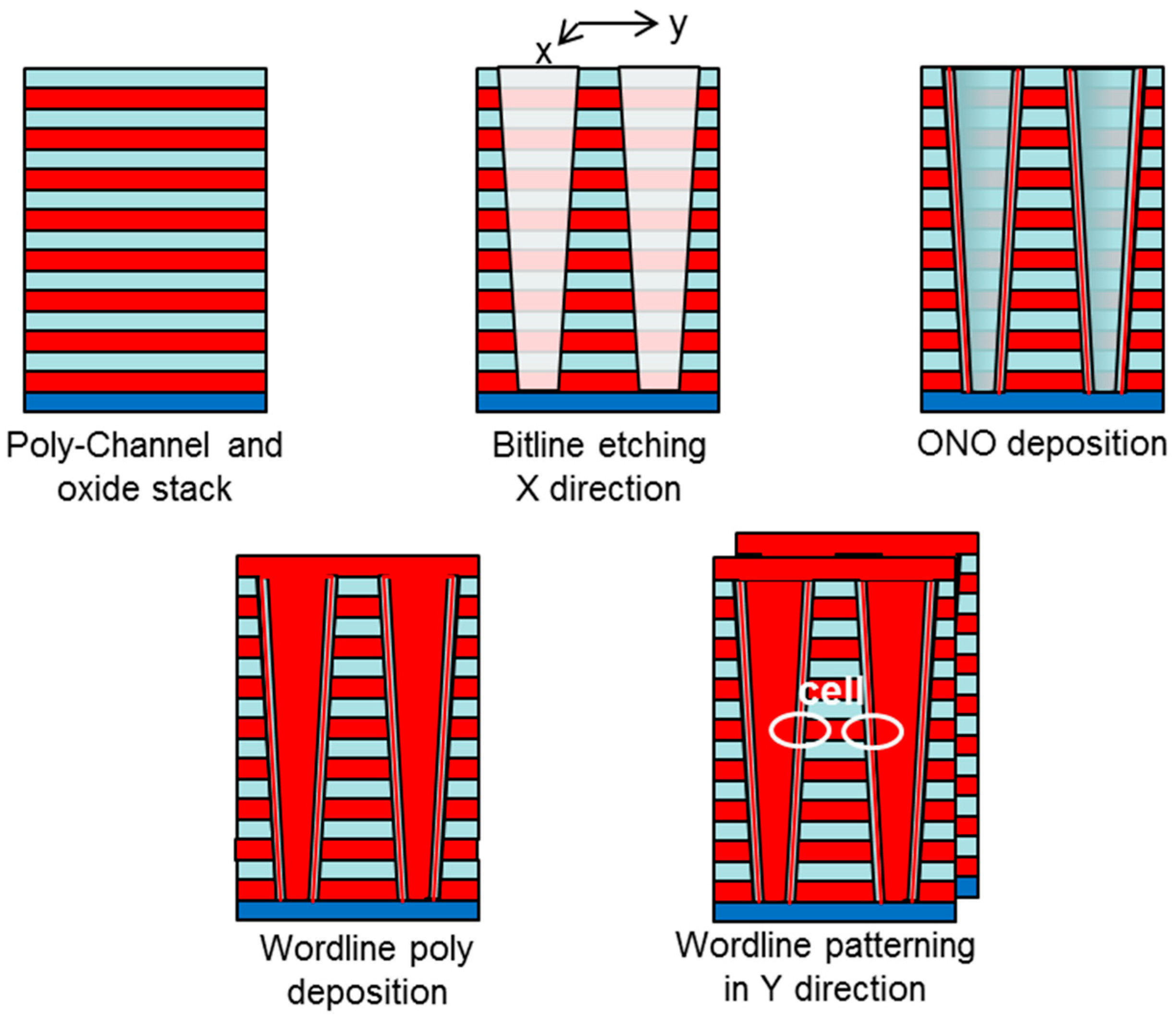
As explained by Figure 1c, a vertical gate (horizontal channel) can be also realized by starting from a poly/oxide stack. In Figure 4, a simplified process sequence to form a vertical-gate 3D NAND is sketched. First, an etching step defines the horizontal channels (the poly of the stack is now used for the channel); then, Oxide/Nitride/Oxide (ONO) layers are deposited along the sidewalls of the etched lines; afterwards, a polysilicon gate can be formed by wrapping around the vertical stack, thus realizing the wordlines and the strings. Another etching step in the opposite direction is used to define the wordlines. The wordlines are wrapped around the channel stack so that the cell transistors are double FinFET structures, as highlighted in Figure 4. It can be noted that the NAND string is horizontal, and the current flows horizontally in the x-direction and is collected by a proper connecting structure (not shown in Figure 4).
From this preliminary introduction, it can be noted that there are two main approaches to make the basic cell structure in 3D NAND: the cell can be of GAA type—made of a circular TFT—or the cell can be a planar TFT. In the following sections, we distinguish between the 3D NAND architectures of these two categories: those using GAA cells and those using planar cell structures.
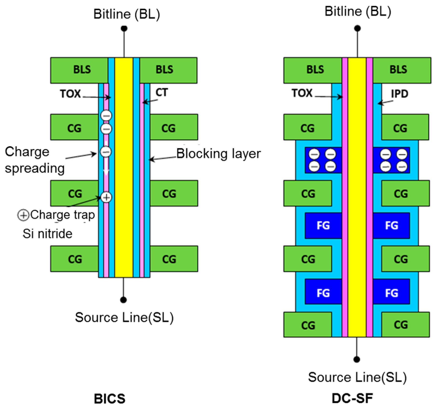
3. The Storage Method: Transitioning from Floating Gate to Charge Trap
In 2D NAND, the basic cell structure is based on a floating gate (FG), where an insulated polysilicon structure between the gate and the channel, the FG, is used to store the electrons. An alternative type of flash cell is the charge-trap (CT) cell, for which the charges are stored in the trapping oxide built between the channel and the gate.
A FG has been the common approach for 2D NAND for over 20 years [6], offering reliable operation and, despite the complex structure, has still been manufactured down to below 16 nm. CT cells have already been proposed as a suitable candidate to replace FGs below 40 nm but finally have not been used in 2D NAND [7,8,9,10,11,12].
For over a decade, several structures have been studied to build the most effective and simpler 3D NAND process. In order to simplify the cell structure, a precondition to be able to scale to multiple layers easily and the use of a CT flash cell was often proposed, and these are now at the base of most 3D NAND architectures. However, some manufacturers still pursue a 3D FG structure, despite it being more complex.
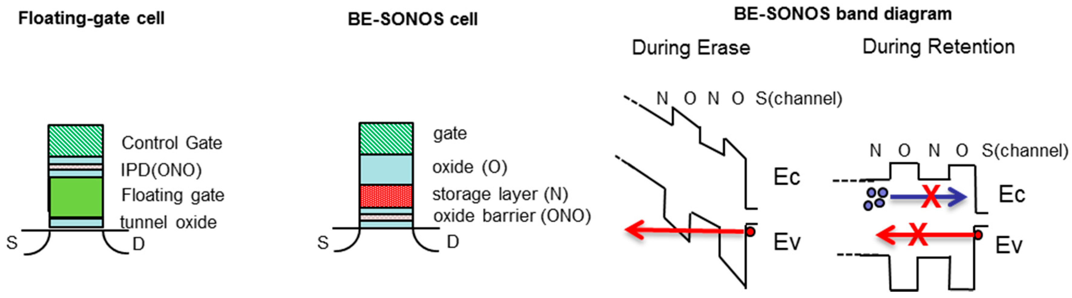
The typical CT NAND cell is a SONOS (silicon/oxide/nitride/oxide/silicon)-type, for which SiO2/SiN/SiO2 layers compose the trapping oxide structure below the polysilicon gate. The drawback of SONOS-type devices is the leakage of trapped charges through the tunnel oxide, made very thin in order to allow direct tunneling. Several innovations have allowed for improving the basic SONOS structure. For example, the use of a combination of a Hi–K metal gate and thicker oxide to improve both retention and erasing has been studied. Barrier Engineered (BE-SONOS) approach to CT [7,8,9,10,11,12] consists of replacing the trapping oxide with a stack of layers, O/N/O/N/O, so as to modify the band structure of the oxide in order to reduce the unwanted drawbacks of the structure (Figure 5).
By proper barrier engineering, the improvement of charge (hole) injection for both erasing and retention has been demonstrated; moreover, the reduction of gate injection, producing erase saturation, is possible, even in GAA devices [13]. Several variants of oxide and even the combination with a metal gate and Hi–K could be employed in CT devices [5,10].
4. 3D NAND with GAA Cell Structure
In this chapter, three 3D NAND architectures using a circular-gate GAA cell are described. The first two are based on a CT device (PBICS and VNAND) and the third is based on a FG device.
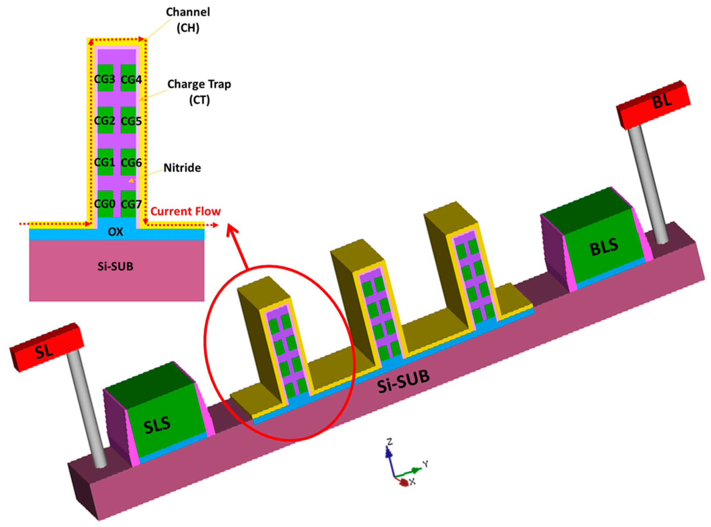
4.1. Pipe-Shaped Bit Cost Scalable (PBICS) Architecture
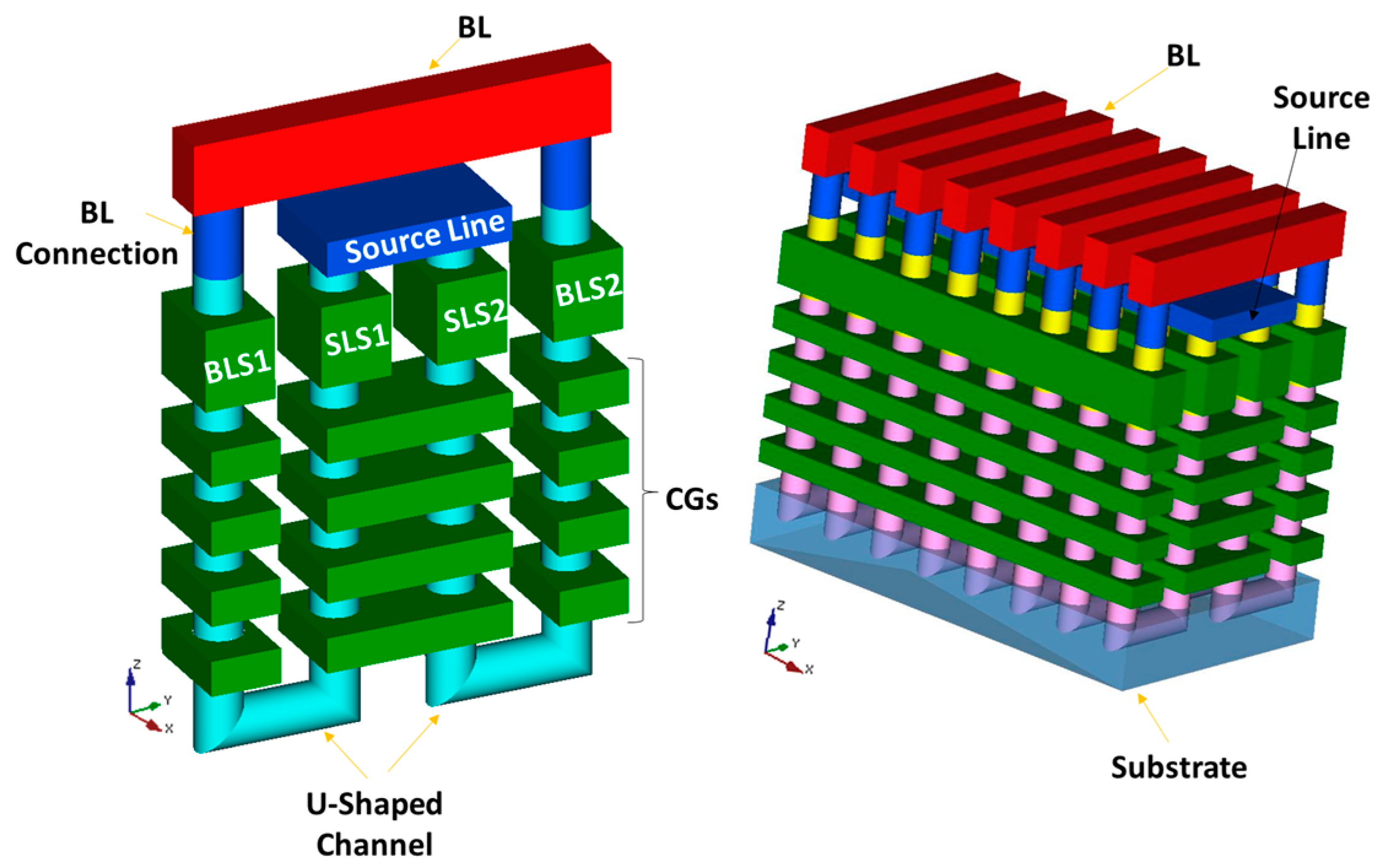
PBICS architecture [14] is a derivation of bit-cost scalable (BiCS) [15,16]; both are based on a vertical channel GAA device. The PBICS structure is composed of two pillars that are shorted at the bottom side by a pipe connection (Figure 6). The resulting structure can thus be contacted only on the top layers, namely the bitline and the sourceline, avoiding the bottom source connection, which is more complicated to realize from the process side and which would also introduce a higher source resistance to be handled with proper strapping sections.
The advantages of PBICS structures compared to BiCS are the following: (1) better controlled String Line Select (SLS) transistors, (2) better sourceline connection realized with backend metal lines, and (3) more reliable ONO with respect to the bottom source side that would require special process steps to prevent its degradation [14].
Proper optimization of the process sequences, together with the use of a thin-film transistor structure (Macaroni structure), allows for achieving vertical devices with very good performance despite the difficulties of a gate-first process.
The wordline fan-out is realized by staircase formation.
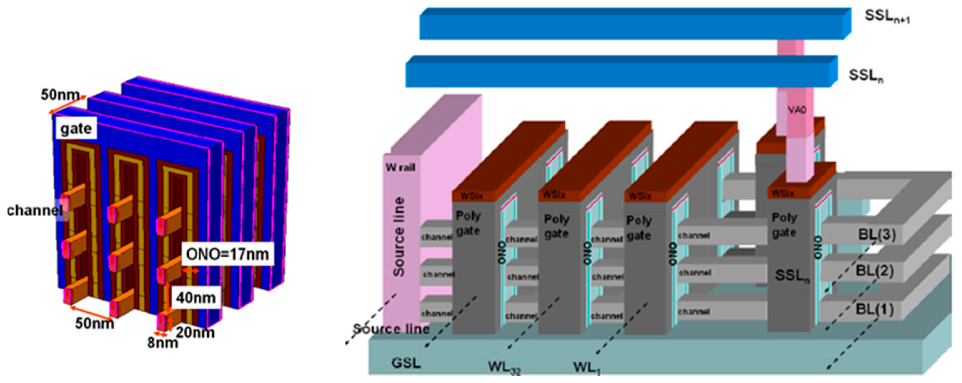
4.2. The V-NAND Architecture
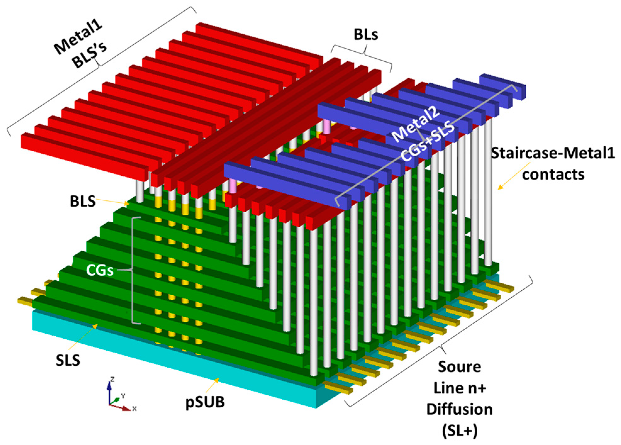
A V-NAND structure is also a GAA vertical-type cell [17,18]. It is derived from the original TCAT architecture [19].
The V-NAND structure is also made with a punch-and-plug process and employs a bottom source. The complexity is given by tuning and operating the bottom SLS transistors and the source line n+ resistance. From the bitline side, it has a simple connection to the metal backend. A staircase structure is used to build the connection to the wordlines and to select gates, which is common in 3D NAND (Figure 7).
The hole trenches can be arranged in a staggered fashion, as shown in Figure 7. The staggering allows for optimizing the area occupation, decreasing the bitline metal pitch and increasing the cell density.
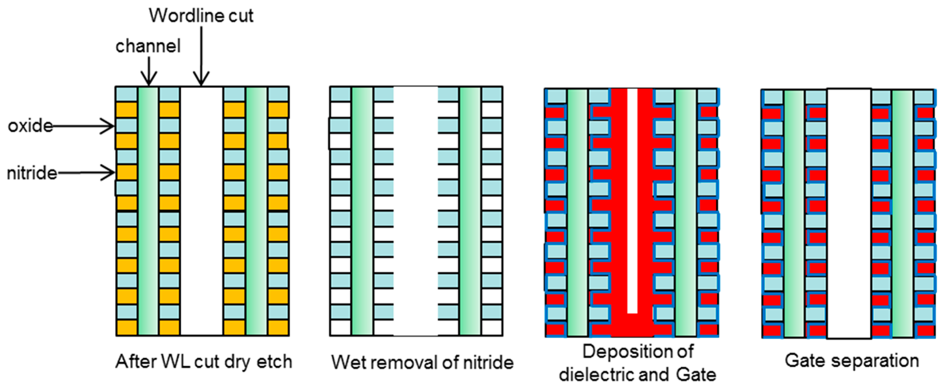
In the process proposed for TCAT architecture [19], a layer stack is not formed by polysilicon/oxide but rather by sacrificial nitride/oxide (Figure 8), because the process is gate-last and requires etching for gate replacement (Figure 8). A polysilicon filler is deposited after the punch process. After wordline cut, a wet removal of the nitride is followed by gate-dielectric and metal-gate deposition. Thus, the resulting process has a more conventional gate-last order with respect to PBICS and also employs Hi–k and a metal gate to optimize the CT operation and wordline resistance. VNAND also makes use of some barrier-engineered materials, according to literature [18].
4.3. The Floating-Gate Cell Architectures
A FG vertical cell is also proposed, with several options [20,21,22,23]. The reasons for pursuing a FG structure in 3D NAND are due to the advantages of FG versus CT cells and the industry’s familiarity with the former in terms of 2D NAND history.
A FG cell requires a more complex process structure; in fact, the deposition of an interpoly dielectric (IPD) and FG in between control-gate poly layers is necessary. The layer stack is therefore made of sacrificial nitride and polysilicon for gate replacement.
From the etched holes, FG areas are selectively etched and then an IPD and FG are formed by deposition. Finally, the tunnel oxide and the polysilicon channel are deposited. The peculiarity of the process for a vertical FG device is the formation of the FG and of course the formation of an IPD. This approach can also be considered gate-first, where critical tunnel oxide is grown before channel deposition. Critical parameters for the FG cell operation are the coupling ratio between the CG and FG and FG–FG coupling. Complex structures have been proposed in order to optimize such issues [24].
FG structures aim to cope with drawbacks of CT, such as erasing speed, poor retention and charge spreading [20] between cells along the CT nitride. The FE effect due to the GAA structure allows for enhancing of the “coupling” between the CG and FG, which is key for the FG; however, the strong electric field through the oxides is also a reliability concern.
5. 3D NAND with Planar Cell Structure
In the previous section, we have seen that the most common 3D structures are based on a GAA circular gate, either CT or FG. Nonetheless, other approaches, using planar devices and not using the GAA punch-and-plug process, have been demonstrated as well. A 3D planar structure has been proposed in many architectures for building NAND strings with a vertical gate (and horizontal or even vertical channels). These structures very often employ a WL-BL patterning scheme that is similar to that of 2D NAND.
In this chapter, we review some 3D NAND options that are based on planar cell structures.
5.1. Vertical-Stacked-Array-Transistor (VSAT) Architecture
VSAT [25] (Figure 10) was proposed as a simple and straightforward process to achieve 3D strings by simple patterning and etching, and likewise for 2D NAND. In the VSAT approach, the doped polysilicon of the stack forms the gates. The stack is then etched by proper patterning and the gates are exposed; afterwards, the tunnel oxide and charge-trapping layers are deposited, followed by polysilicon forming the channel. Another etching step defines the strings. It is to be noted that the process is also gate-first channel-last, which is different to 2D NAND. In this structure, a Chemical-Mechanical Planarization process is able to expose all the wordline/polysilicon layers and allow for a straightforward connection to the wordlines, which is also a key issue for 3D NAND. Another advantage of the structure was to realize Gate-Select-Line (GSL) and String-Select-Line (SSL) transistors on the substrate instead of in the vertical stack, thus easing the tuning of those select gates, which is a critical point for 3D structures. The TFT used a 20 nm film, essentially to make a fully depleted channel, which was a key item to resolve the previously mentioned issues derived from the polysilicon grain boundary, and thus improved the subthreshold slope.
The efficiency of VSAT is not excellent in terms of area and performance, because the channel passes through the same cell twice and because of the external planar select gate; however, it shows the possibility of realizing 3D NAND with standard etching and planar cells.
5.2. Vertical Gate-Type Architectures
A vertical gate (VG) approach has also been proposed [26,27,28], whereby the role of the control-gate and the channel can be reverted substantially with respect to vertical-channel structures.
The VG architecture uses a WL-BL patterning scheme, which is more similar to 2D NAND than the punch-and-plug process. The architecture is more scalable in 2D with respect to the vertical trench approaches, because the latter has to keep a minimum trench size and pitch, while the former has only one critical step per each direction. The VG base cell has a size of 4F2 and studies have shown the scalability to be possibly as low as 25 nm.
The 3D VG is based on a junction-free buried channel. The transistor is a double VG TFT with a BE-SONOS structure in a depletion-mode buried channel to improve the transistor current, and it has a junction-free structure.
Figure 11 shows an implementation of VG-type 3D NAND with an island gate for SSL select transistors. The connection of bitlines to metal layers is not shown. For VG 3D NAND, the formation of the strings is quite straightforward; the wordline and sourceline resistance is managed easily, however the connection to the bitline and the string selection is more complicated compared to vertical channel. In [29,30] a simple method for SSL transistor formation is proposed; this is a special connecting structure from the horizontal polysilicon string channels to the metal bitlines, and it optimizes the layout of the select transistors.
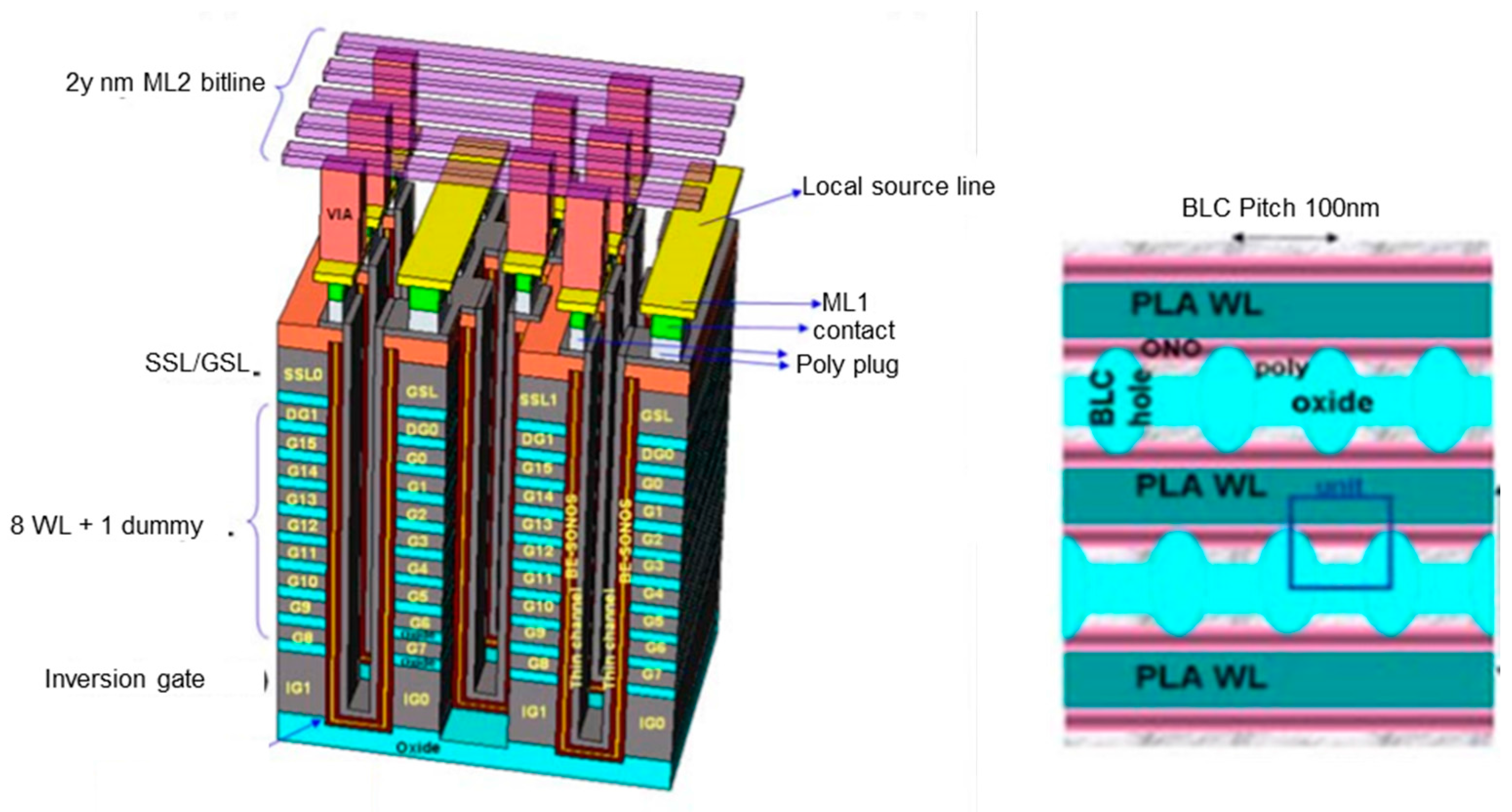
5.3. Single-Gate Vertical Channel (SGVC) Architecture
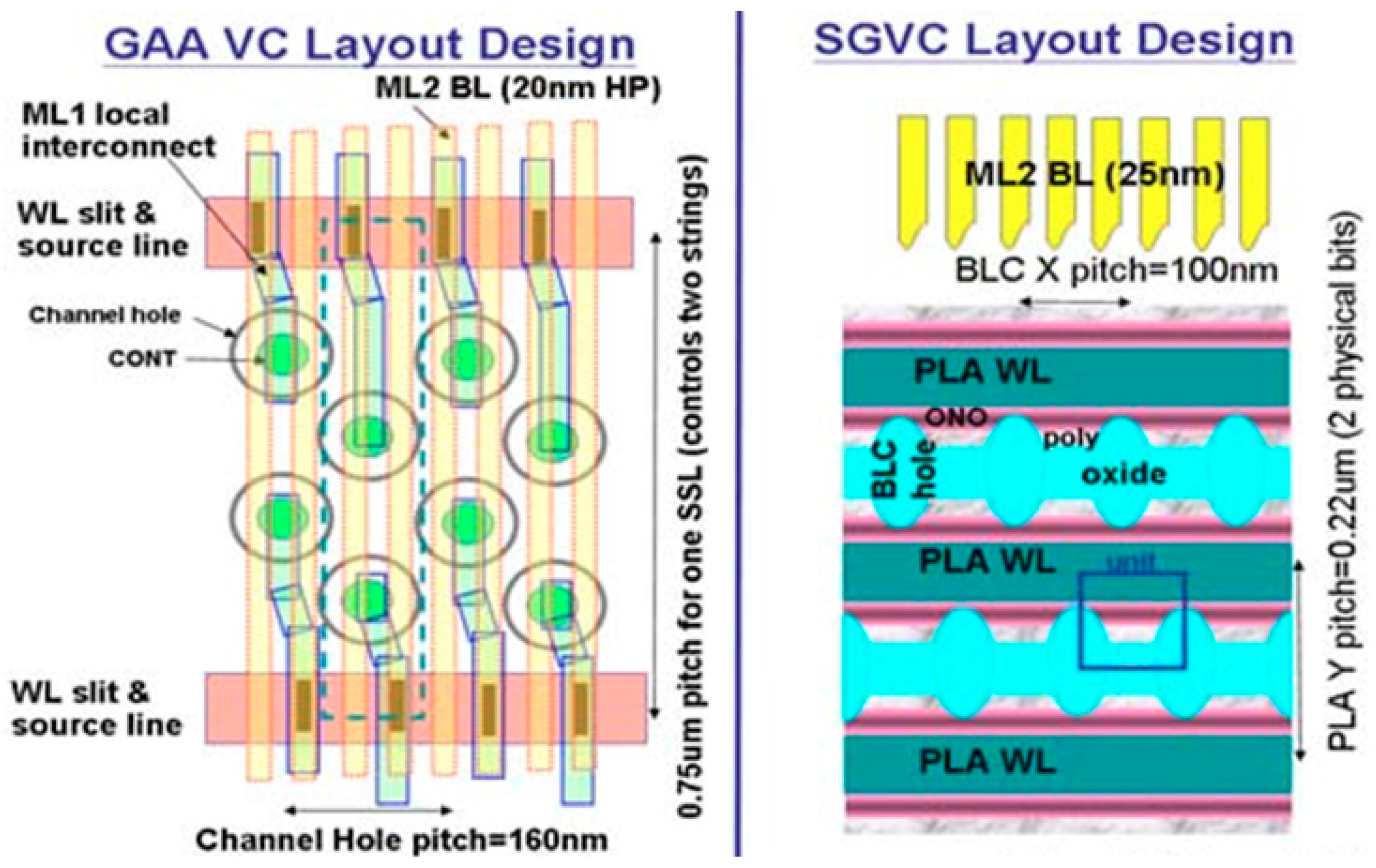
A SGVC [33] is also based on a flat-channel TFT cell. For a SGVC (Figure 12), the charge-trapping layers and the thin-channel are deposited on the sidewalls of a wordline trench; a bitline cut (BLC) is necessary in order to separate the bitlines and to form the strings. The BLC can be seen better in the top view of Figure 12. The interesting feature of this structure is that two channels are formed on the sidewalls of the wordline trench and are controlled by independent wordlines; therefore, there are double the number of transistors in a trench compared to GAA structures. The SGVC structure is also naturally a bottom U-turn-type, as a result of the poly deposition process step. However, a SGVC with a bottom source structure has also been investigated [2]. Bitline and source contacts are connected to the two metal layers’ backend in straightforward manner. In between the two U-turn-type strings, the BLC, which is used to define the width of the strings in the x-direction, is also visible. The twisted layout of the BLC, as shown in the top view, allows for a twisted connection to the bitlines, thus allowing a 25 nm half-pitch for Metal2 bitlines.
The cell of the SGVC is an ultra-thin-body TFT and shows performances that are similar or even better than the Macaroni-type GAA-device. In fact, the structure of the TFT remains flat even if the vertical etching has any taper angle and it retains the same performance; this is in contrast with GAA cells, for which the taper angle determines variations in the cell curvature and thus variations in the cell characteristics. The flat-body cell is therefore insensitive to the Critical Dimention (CD) -etching variations along the vertical string compared to the GAA device, which is dependent on the cell’s curvature; as a consequence, the control of the CD in vertical etching can be less stringent in the SGVC.
For a SGVC, the twisted layout of BLC holes allows for a doubling of the Metal2 bitline pitch to enable a larger page size (Figure 13). The top layout of the SGVC is compared to a GAA VC design in Figure 13. As a result of the optimized layout, double the number of cells per trench and technology shrinks are possible, and it is estimated that SGVC architecture can achieve 2 to 4 times the density of a GAA VC for the same number of layers.
6. Comparison between CT Flat Cell and GAA Cell Structures
In this section 3D NAND flat-cell architectures are compared to GAA cell architectures by highlighting the basic production process characteristics. It must be noted here that the overall performance of the 3D NAND architectures should be finally evaluated after a proper system implementation. In fact, several drawbacks of an architecture can be corrected or mitigated by implementing ad hoc program algorithms and ECC [4,17,31,32,34,35,36,37].
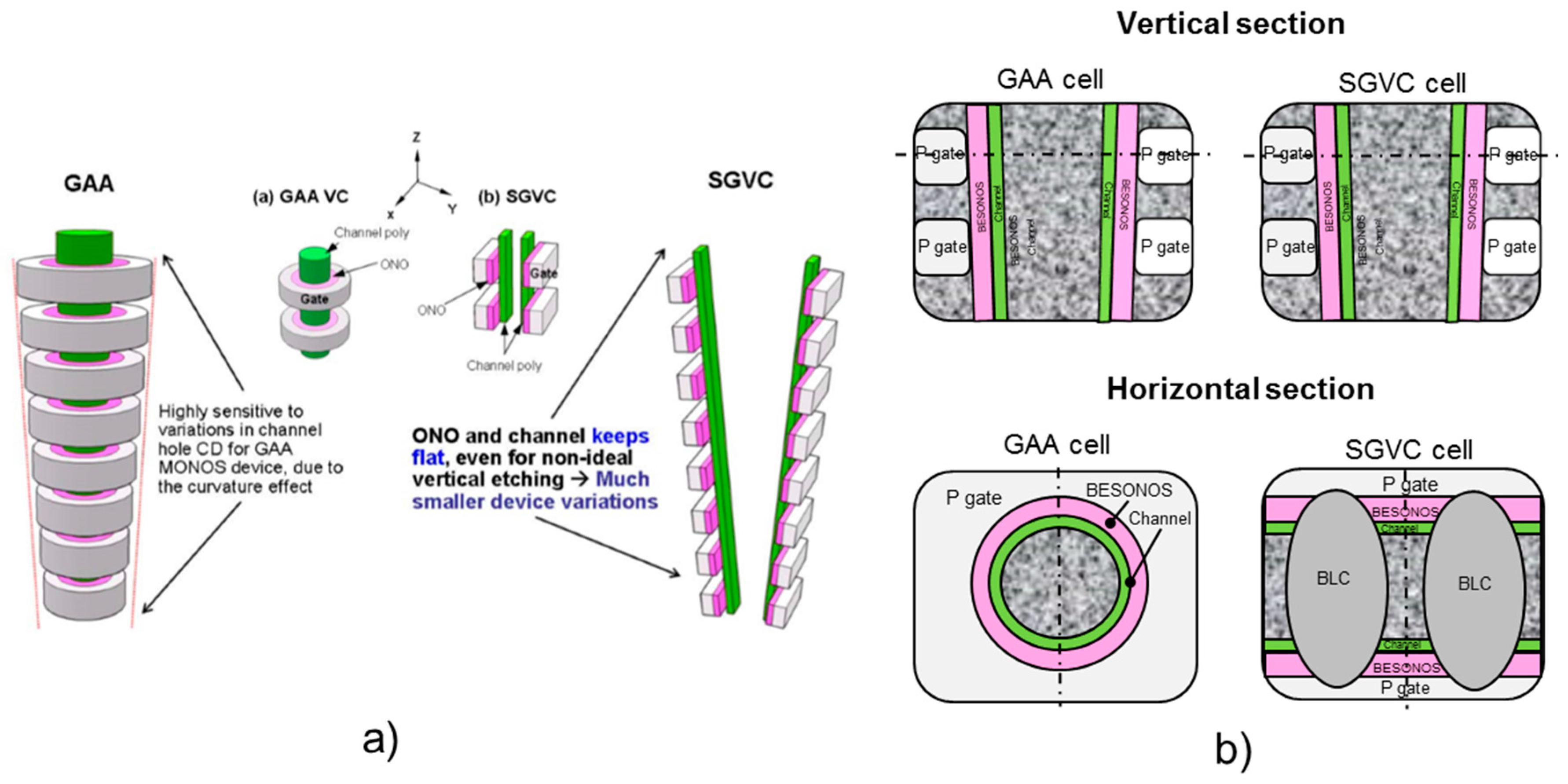
GAA (vertical channel) cells are sensitive to curvature variations because of the electric FE effect. Geometrical layer-to-layer variations are intrinsic in the plug process as a result of the vertical-trench etching difficulty and the fact that the plug has a cone shape rather than a cylindrical shape. Therefore, cells of each layer are subjected to a different FE strength by construction. These variations cause difficulties in obtaining a tight Vth distribution and maintain the margin between the Vth states; they have to be handled properly by programming algorithms as much as possible. The uniformity of the trench has to be controlled tightly when the number of layers is increased. From this perspective, architectures based on an almost-planar cell structure, such as SGVC, have more regular cell-to-cell behavior. A tight control of CD uniformity in the trench and a regular polysilicon structure are essential in order to increase the number of layers.
In Figure 14a, a vertical string of a GAA VC structure and the planar structure of SGVC are shown. In the GAA structure, the variations of the holes’ size from top to bottom cause variation in the cell behavior, as explained. In the SGVC structure, the channel remains flat even with weaker control on the vertical etching, resulting in a better control of the device compared to the GAA strings. In the planar device, the structure remains nearly planar independently from the vertical taper angle of the punched holes. As a consequence, in the SGVC it should be easier to increase the number of layers.
In VG-type 3D NAND, the etching steps are more similar to 2D NAND and also use a planar cell structure. VG-type NAND has a good scalability for the critical features and this also allows for increasing the density, with less layers compared to VC GAA structures.
In a GAA CT cell, it is essential to have a thin body (of Macaroni type) in order to make the TFT device fully depleted, minimizing the negative effects of grain boundary silicon traps. Similarly, the flat-cell single-gate device is also realized with an ultra-thin body of less than 8 nm. As a result, both the GAA CT Cell and flat cell can take advantage of the thin-body TFT advantages [33].
Figure 14b shows a cross-section of a SGVC cell and a GAA cell; it is shown that the cells in fact have the same device structure when looking through a vertical cross-section. In the plane section view, it is highlighted that the cell is in fact planar in the SGVC, while it is circular in the GAA. The BLC does not significantly affect the cell’s performance. In fact, the BLC size can be reduced as much as possible in order to shrink the cell in 2D. On the contrary, the size of the GAA cell built around the vertical trench cannot be reduced significantly.
Regarding the Vth memory window, the SGVC shows an excellent window and can also achieve excellent layer-to-layer operation uniformity that allows for increasing the number of layers. The wordline interference (Z-interference) is dominant, but it could be minimized primarily by an increase of the inter-wordline oxide of the oxide/poly stack. By applying wordline iteration techniques, a sufficient margin for TLC operation for the SGVC has been demonstrated [38].
The 3D VG NAND, which also belongs to the category of planar cells, was also studied thoroughly regarding interference effects and multilevel capability, and similar results showed that TLC operation is achievable as well.
In 3D GAA-based NAND, the interference effects can also be managed by proper algorithms. However, 3D FG NAND has an advantage over CT cells, as the FG cells in the 3D configuration are less susceptible to interferences.
Table 1 summarizes the key factors of the various 3D NAND architectures presented in this article.
7. Conclusions
The challenge of 3D NAND is to prove both its large-scale manufacturability and diminishing unit cost. The most common GAA structures have limitations for the cell’s pitch and therefore the only way to increase the cell planar density is to increase the number of layers. At the same time, the vertical etch control has to be very tight to maintain uniformity between the layers, which prevents obtaining a fairly good Vth distribution for multilevel operation.
Other approaches, employing a flat-body cell, promise excellent scalability, combining the advantages of a flat cell, which is less sensitive to the geometrical variations in vertical etching, and can achieve excellent performance. Moreover, the SGVC structure can also achieve a better cell density, compared to GAA approach, with the same number of layers.
Conflicts of Interest
The author declares no conflict of interest.
References
- Fukuzumi, Y.; Katsumata, R. Optimal Integration and Characteristics of Vertical Array Devices for Ultra-High Density, Bit-Cost Scalable Flash Memory. In Proceedings of the International Electron Devices Meeting (IEDM), Washington, DC, USA, 10–12 December 2007; pp. 449–452. [Google Scholar]
- Lai, S.-C.; Lue, H.-T.; Hsu, T.-H.; Wu, C.-J.; Liang, L.-Y.; Du, P.-Y.; Chiu, C.-J.; Lu, C.Y. A Bottom-Source Single-Gate Vertical Channel (BS-SGVC) 3D NAND Flash Architecture and Studies of Bottom Source Engineering. In Proceedings of the 8th International Memory Workshop (IMW), Paris, France, 15–18 May 2016. [Google Scholar]
- Hsiao, Y.H.; Lue, H.T.; Chen, W.-C.; Chen, C.-P.; Chang, K.-P.; Shih, Y.-H.; Tsui, B.-Y.; Lu, C.-Y. Modeling the Variability Caused by Random Grain Boundary and Trap-location Induced Asymmetrical Read Behavior for a Tight-pitch Vertical Gate 3D NAND Flash Memory Using Double-Gate Thin-Film Transistor (TFT) Device. In Proceedings of the International Electron Device Meeting (IEDM), San Francisco, CA, USA, 10–13 December 2012. [Google Scholar]
- Micheloni, R. 3D Flash Memories; Springer: Dordrecht, Netherlands, 2016. [Google Scholar]
- Hsiao, Y.H.; Lue, H.T. A Critical Examination of 3D Stackable NAND Flash Memory Architectures by Simulation Study of the Scaling Capability. In Proceedings of the International Memory Workshop (IMW), Seoul, Korea, 16–19 May 2010. [Google Scholar]
- Masuoka, F.; Momodomi, M.; Iwata, Y.; Shirora, R. New ultra high density EPROM and flash EEPROM with NAND structured cell. In Proceedings of the International Electron Devices Meeting (IEDM), Washington, DC, USA, 6–9 December 1987; pp. 552–555. [Google Scholar]
- Hsu, T.-H.; Lue, H.T.; King, Y.-C.; Hsieh, J.-Y.; Lai, E.-K.; Hsieh, K.-Y.; Liu, R.; Lu, C.-Y. A High-Performance Body-Tied FinFET Bandgap Engineered SONOS (BE-SONOS) for nand-Type Flash Memory. IEEE Electr. Device Lett. 2007, 28, 443–445. [Google Scholar] [CrossRef]
- Lue, H.T.; Wang, S.Y.; Hsiao, Y.-H.; Lai, E.-K.; Yang, L.-W.; Yang, T.; Chen, K.-C.; Hsieh, K.-Y.; Liu, R.; Lu, C.Y. Reliability model of bandgap engineered SONOS (Be-SONOS). In Proceedings of the International Electron Devices Meeting (IEDM), San Francisco, CA, USA, 11–13 December 2006; pp. 495–498. [Google Scholar]
- Lue, H.T.; Wang, S.-Y.; Lai, E.-K.; Hsieh, K.-Y.; Liu, R.; Lu, C.Y. A BE-SONOS (Bandgap Engineered SONOS) for post-floating gate era flash memory. In Proceedings of the International Symposium on VLSI Technology, Systems and Applications (VLSI-TSA), Hsinchu, Taiwan, 23–25 April 2007; pp. 1–4. [Google Scholar]
- Liu, R.; Lue, H.-T.; Chen, K.C.; Lu, C.-Y. Reliability of barrier engineered charge trapping devices for sub-30 nm NAND flash. In Proceedings of the International Electron Devices Meeting (IEDM), Baltimore, MD, USA, 7–9 December 2009. [Google Scholar]
- Lue, H.-T.; Lo, R.; Hsieh, C.-C.; Du, P.-Y.; Chen, C.-P.; Hsu, T.-H.; Chang, K.-P.; Shih, Y.-H.; Lu, C.-Y. A Novel Double-Trapping BE-SONOS Charge-Trapping NAND Flash Device to Overcome the Erase Saturation without Using Curvature-Induced Field Enhancement Effect or High-K (HK)/Metal Gate (MG) Materials. In Proceedings of the International Electron Devices Meeting (IEDM), San Francisco, CA, USA, 15–17 December 2014. [Google Scholar]
- Lo, R.; Du, P.-Y.; Hsu, T.-H.; Wu, C.-J.; Guo, J.-Y.; Cheng, C.-M.; Lue, H.-T.; Shih, Y.-H.; Hou, T.-H.; Hsieh, K.-Y.; et al. A Study of Blocking and Tunnel Oxide Engineering on Double-Trapping (DT) BE-SONOS Performance. In Proceedings of the International Memory Workshop (IMW), Monterey, CA, USA, 17–20 May 2015. [Google Scholar]
- Nitayama, A.; Aochi, H. Bit Cost Scalable (BiCS) Flash Technology for Future Ultra High Density Storage Devices. In Proceedings of the International Symposium on VLSI Technology Systems and Applications (VLSI-TSA), Hsinchu, Taiwan, 26–28 April 2010. [Google Scholar]
- Katsumata, R.; Kito, M.; Fukuzumi, Y.; Kido, M.; Tanaka, H.; Komori, Y.; Ishiduki, M.; Matsunami, J.; Fujiwara, T.; Nagata, Y.; et al. Pipe-shaped BiCS Flash Memory with 16 Stacked Layers and Multi-Level-Cell Operation for Ultra High Density Storage Device. In Proceedings of the Symposium on VLSI Technology, Honolulu, HI, USA, 16–18 June 2009. [Google Scholar]
- Tanaka, H.; Kido, M.; Yahashi, K.; Oomura, M.; Katsumata, R.; Kito, M.; Fukuzumi, Y.; Sato, M.; Nagata, Y.; Matsuoka, Y.; et al. Bit Cost Scalable Technology with Punch and Plug Process for Ultra High Density Flash Memory. In Proceedings of the Symposium on VLSI Technology, Kyoto, Japan, 12–14 June 2007. [Google Scholar]
- Aochi, H. BICS Flash as a Future 3D Non-volatile Memory Technology for Ultra High Density Storage Devices. In Proceedings of the International Memory Workshop (IMW), Monterey, CA, USA, 10–14 May 2009. [Google Scholar]
- Park, K.T.; Han, J.; Kim, D.; Nam, S.; Choi, K.; Kim, M.-S.; Kwak, P.; Lee, D.; Choi, Y.-H.; Kang, K.-M.; et al. Three-dimensional 128Gb MLC vertical NAND Flash-memory with 24-WL stacked layers and 50MB/s high-speed programming. In Proceedings of the International Solid-State Circuits Conference Digest of Technical Papers (ISSCC), San Francisco, CA, USA, 9–13 February 2014. [Google Scholar]
- Park, K.T.; Byeon, D.S. A world's first product of three-dimensional vertical NAND Flash memory and beyond. In Proceedings of the 14th Annual Non-Volatile Memory Technology Symposium (NVMTS), Jeju Island, Korea, 27–29 October 2014. [Google Scholar]
- Jang, J.; Kim, H.S.; Cho, W.; Cho, H.; Kim, J.; Shim, S.I.; Younggoan; Jeong, J.-H.; Son, B.-K.; Kim, D.W.; et al. Vertical Cell Array using TCAT(Terabit Cell Array Transistor) Technology for Ultra High Density NAND Flash Memory. In Proceedings of the Symposium on VLSI Technology, Honolulu, HI, USA, 16–18 June 2009. [Google Scholar]
- Whang, S.J.; Lee, K.; Shin, D.; Kim, B.Y.; Kim, M.; Bin, J.; Han, J.; Kim, S.; Lee, B.; Jung, Y.; et al. Novel 3-Dimensional Dual Control-Gate with Surrounding Floating-Gate (DC-SF) NAND Flash Cell for 1Tb File Storage Application. In Proceedings of the International Electron Devices Meeting (IEDM), San Francisco, CA, USA, 6–8 December 2010; pp. 668–671. [Google Scholar]
- Parat, K.; Dennison, C. A Floating Gate Based 3D NAND Technology with CMOS Under Array. In Proceedings of the International Electron Devices Meeting (IEDM), Washington, DC, USA, 7–9 December 2015. [Google Scholar]
- Seo, M.S.; Park, S.-K.; Endoh, T. The 3-dimensional vertical FG nand flash memory cell arrays with the novel electrical S/D technique using the extended sidewall control gate (ESCG). In Proceedings of the International Memory Workshop, Seoul, Korea, 16–19 May 2010; pp. 1–4. [Google Scholar]
- Tanaka, T.; Helm, M.; Vali, T.; Ghodsi, R.; Kawai, K.; Park, J.-K.; Yamada, S.; Pan, F.; Einaga, Y.; Ghalam, A.; et al. 7.7 A 768Gb 3b/cell 3D-floating-gate NAND flash memory. In Proceedings of the 2016 IEEE International Solid-State Circuits Conference (ISSCC), San Francisco, CA, USA, 31 January–4 February 2016; pp. 142–144. [Google Scholar]
- Noh, Y.; Ahn, Y.; H, Y.; Han, B.; Chung, S.; Shim, K.; Lee, K.; Kwak, S.; Shin, S.; Choi, I.; et al. A new metal control gate last process (MCGL process) for high performance DC-SF (dual control gate with surrounding floating gate) 3D NAND flash memory. In Proceedings of the Symposium on VLSI Technology, Honolulu, HI, USA, 12–14 June 2012; pp. 19–20. [Google Scholar]
- Kim, J.; Hong, A.J.; Kim, S.M.; Song, E.B.; Park, J.H.; Han, J.; Choi, S.; Jang, D.; Moon, J.-T.; Wang, L.K. Novel Vertical-Stacked-Array-Transistor (VSAT) for ultra-high-density and cost-effective NAND Flash memory devices and SSD (Solid State Drive). In Proceedings of the Symposium on VLSI Technology, Honolulu, HI, USA, 16–18 June 2009. [Google Scholar]
- Kim, W.; Choi, S.; Sung, J.; Lee, T.; Park, C.; Ko, H.; Jung, J.; Yoo, I.; Park, Y. Multi-Layered Vertical Gate NAND Flash Overcoming Stacking Limit for Terabit Density Storage. In Proceedings of the Symposium on VLSI Technology, Honolulu, HI, USA, 16–18 June 2009. [Google Scholar]
- Lue, H.T.; Hsu, T.H.; Hsiao, Y.-H.; Hong, S.P.; Wu, M.T.; Hsu, F.H.; Lien, N.Z.; Wang, S.-Y.; Hsieh, J.-Y.; Yang, L.-W.; et al. A Highly Scalable 8-Layer 3D Vertical-Gate (VG) TFT NAND Flash Using Junction-Free Buried Channel BE-SONOS Device. In Proceedings of the VLSI Symposia on Technology, Honolulu, HI, USA, 15–17 June 2010. [Google Scholar]
- Sakuma, K.; Kusai, H.; Fujii, S.; Koyama, M. Highly Scalable Horizontal Channel 3-D NAND Memory Excellent in Compatibility With Conventional Fabrication Technology. IEEE Electr. Device Lett. 2013, 34, 1142–1144. [Google Scholar] [CrossRef]
- Chen, S.H.; Lue, H.T.; Shih, Y.-H.; Chen, C.-F.; Hsu, T.-H.; Chen, Y.-R.; Hsiao, Y.-H.; Huang, S.-C.; Chang, K.-P.; Hsieh, C.-C.; et al. A Highly Scalable 8-layer Vertical Gate 3D NAND with Split-page Bit Line Layout and Efficient Binary-sum MiLC (Minimal Incremental Layer Cost) Staircase Contacts. In Proceedings of the International Electron Device Meeting (IEDM), San Francisco, CA, USA, 10–13 December 2012. [Google Scholar]
- Yeh, T.H.; Wu, C.-J.; Hu, C.-W.; Chen, W.-C.; Lue, H.-T.; Shih, Y.-H.; King, Y.-C.; Lu, C.-Y. A New String Decoding Scheme for Enhancing Array Block Efficiency of Vertical Gate Type (VG-Type) 3-D NAND. IEEE Electr. Device Lett. 2015, 36, 330–332. [Google Scholar] [CrossRef]
- Hsieh, C.C.; Lue, H.T.; Li, Y.C.; Chang, K.-P.; Lu, H.C.; Li, H.-P.; Chen, W.-C.; Hsiao, Y.-H.; Hung, S.-N.; Chen, T.-W.; et al. Study of the Interference and Disturb Mechanisms of Split-Page 3D Vertical Gate (VG) NAND Flash and Optimized Programming Algorithms for Multi-level Cell (MLC) Storage. In Proceedings of the Symposium on VLSI Technology (VLSIT), Kyoto, Japan, 11–13 June 2013. [Google Scholar]
- Hung, C.H. Layer-Aware Program-and-Read Schemes for 3D Stackable Vertical-Gate BE-SONOS NAND Flash Against Cross-Layer Process Variations. IEEE J. Solid State Circuits 2015, 50, 1491–1501. [Google Scholar] [CrossRef]
- Lue, H.T.; Hsu, T.H.; Wu, C.-J.; Chen, W.-C.; Yeh, T.-H.; Chang, K.-P.; Hsieh, C.-C.; Du, P.-Y.; Hsiao, Y.-H.; Jiang, Y.-W.; et al. A novel double-density single gate vertical channel (SGVC) 3D NAND that is tolerant to deep vertical etching CD variation and possesses robust read-disturb immunity. In Proceedings of the International Electron Devices Meeting (IEDM), Washington, DC, USA, 7–9 December 2015. [Google Scholar]
- Wang, Y.; Shao, Z.; Chan, H.C.B.; Bathen, L.A.D.; Dutt, N.D. A Reliability Enhanced Address Mapping Strategy for Three-Dimensional (3-D) NAND Flash Memory. IEEE Trans. VLSI-Syst. 2014, 22, 2402–2410. [Google Scholar] [CrossRef]
- Wang, Y.; Zhang, M.; Yang, J. Temperature-aware data allocation strategy for 3D charge-trap flash memory. In Proceedings of the 22nd ACM/IEEE Asia and South Pacific Design Automation Conference, Chiba, Japan, 16–19 January 2017; pp. 572–577. [Google Scholar]
- Wang, Y.; Dong, L.; Mao, R. P-Alloc: Process-Variation Tolerant Management for 3D Charge-Trapping Flash Memory. In Proceedings of the ACM Transactions on Embedded Computing Systems (TECS), New York, NY, USA, 1–3 October 2017. [Google Scholar]
- Lue, H.-T.; Li, Y.C.; Chen, T.-W.; Li, H.-P.; Lu, C.-Y. A novel dichotomic programming algorithm applied to 3D NAND flash. In Proceedings of the Symposium on VLSI Technology (VLSI Technology), Kyoto, Japan, 16–18 June 2015. [Google Scholar]
- Wu, C.-J.; Lue, H.-T.; Hsu, T.-H.; Hsieh, C.-C.; Chen, W.-C.; Du, P.-Y.; Chiu, C.-J.; Lu, C.-Y. Device Characteristics of Single-Gate Vertical Channel (SGVC) 3D NAND Flash Architecture. In Proceedings of the 8th International Memory Workshop (IMW), Paris, France, 15–18 May 2016. [Google Scholar]
Figure 1.
2D and 3D vertical channel and 3D horizontal channel concepts.

Figure 2.
Punch-and-plug process steps (gate first).

Figure 3.
Macaroni gate-all-around (GAA) cell structure [copyright 2016 by Springer] [4].
Figure 3.
Macaroni gate-all-around (GAA) cell structure [copyright 2016 by Springer] [4].

Figure 4.
Vertical gate simplified process.

Figure 5.
Floating-gate (FG) structure vs barrier-engineered silicon/oxide/nitride/oxide/silicon (BE-SONOS) charge-trap (CT) structure.
Figure 5.
Floating-gate (FG) structure vs barrier-engineered silicon/oxide/nitride/oxide/silicon (BE-SONOS) charge-trap (CT) structure.

Figure 6.
PBiCS structure.

Figure 7.
V-NAND structure [copyright 2016 by Springer] [4].
Figure 7.
V-NAND structure [copyright 2016 by Springer] [4].

Figure 8.
TCAT/V-NAND process.

Figure 9.
BiCS structure compared to 3D dual control gate with surrounding floating gate (DC-SF) [copyright 2016 by Springer] [4].
Figure 9.
BiCS structure compared to 3D dual control gate with surrounding floating gate (DC-SF) [copyright 2016 by Springer] [4].

Figure 10.
VSAT architecture.

Figure 11.
3D vertical-gate (VG) NAND [27].
Figure 11.
3D vertical-gate (VG) NAND [27].

Figure 12.
Single-gate vertical channel (SGVC) [33].
Figure 12.
Single-gate vertical channel (SGVC) [33].

Figure 13.
Layout of gate-all-around (GAA) and single-gate vertical channel (SGVC) structures [33].
Figure 13.
Layout of gate-all-around (GAA) and single-gate vertical channel (SGVC) structures [33].

Figure 14.
Comparison of gate-all-around (GAA) vs single-gate vertical-channel (SGVC) flat cell [33].
Figure 14.
Comparison of gate-all-around (GAA) vs single-gate vertical-channel (SGVC) flat cell [33].


Table 1.
Comparison table of 3D NAND flash types.
| P-BiCS | TCAT/VNAND | 3D-FG | VG | SGVC | |
|---|---|---|---|---|---|
| Cell shape | GAA | GAA | GAA | Planar | Planar |
| Channel | Vertical | Vertical | Vertical | Horizontal | Vertical |
| Storage | CT | CT | FG | CT | CT |
| Gate process | Gate-first | Gate-last | Gate-first | Gate-last | Gate-first |
| Cell size (1) (um2) | 0.03 | 0.03 | 0.03 | 0.0064 | 0.011 |
| 2D scalability | Poor | Poor | Poor | Good | Fairly good |
| Etching difficulty | High | High | Very High | High | Moderately High |
| Advantages | Simple process | Simple process | FG cell | Cell size Planar cell | Simple process cell size Planar cell |
(1) Cell size is a reference value at current state of literature; 2D scalability has to be considered to evaluate the potential of the structure.
© 2017 by the author. Licensee MDPI, Basel, Switzerland. This article is an open access article distributed under the terms and conditions of the Creative Commons Attribution (CC BY) license (http://creativecommons.org/licenses/by/4.0/).
Share and Cite
MDPI and ACS Style
Silvagni, A. 3D NAND Flash Based on Planar Cells. Computers 2017, 6, 28. https://0-doi-org.brum.beds.ac.uk/10.3390/computers6040028
AMA Style
Silvagni A. 3D NAND Flash Based on Planar Cells. Computers. 2017; 6(4):28. https://0-doi-org.brum.beds.ac.uk/10.3390/computers6040028
Chicago/Turabian StyleSilvagni, Andrea. 2017. "3D NAND Flash Based on Planar Cells" Computers 6, no. 4: 28. https://0-doi-org.brum.beds.ac.uk/10.3390/computers6040028
Note that from the first issue of 2016, this journal uses article numbers instead of page numbers. See further details here.