
Recent Advances in WS2 and Its Based Heterostructures for Water-Splitting Applications


1
Materials Science & Technology Program, College of Arts & Sciences, Qatar University, Doha 2713, Qatar
2
Center for Advanced Materials (CAM), Qatar University, Doha 2713, Qatar
*
Author to whom correspondence should be addressed.
Catalysts 2021, 11(11), 1283; https://0-doi-org.brum.beds.ac.uk/10.3390/catal11111283
Submission received: 4 September 2021
/
Revised: 8 October 2021
/
Accepted: 10 October 2021
/
Published: 24 October 2021
Abstract
:The energy from fossil fuels has been recognized as a main factor of global warming and environmental pollution. Therefore, there is an urgent need to replace fossil fuels with clean, cost-effective, long-lasting, and environmentally friendly fuel to solve the future energy crisis of the world. Therefore, the development of clean, sustainable, and renewable energy sources is a prime concern. In this regard, solar energy-driven hydrogen production is considered as an overriding opening for renewable and green energy by virtue of its high energy efficiency, high energy density, and non-toxicity along with zero emissions. Water splitting is a promising technology for producing hydrogen, which represents a potentially and environmentally clean fuel. Water splitting is a widely known process for hydrogen production using different techniques and materials. Among different techniques of water splitting, electrocatalytic and photocatalytic water splitting using semiconductor materials have been considered as the most scalable and cost-effective approaches for the commercial production of sustainable hydrogen. In order to achieve a high yield of hydrogen from these processes, obtaining a suitable, efficient, and stable catalyst is a significant factor. Among the different types of semiconductor catalysts, tungsten disulfide (WS2) has been widely utilized as a catalytic active material for the water-splitting process, owing to its layered 2D structure and its interesting chemical, physical, and structural properties. However, WS2 suffers from some disadvantages that limit its performance in catalytic water splitting. Among the various techniques and strategies that have been constructed to overcome the limitations of WS2 is heterostructure construction. In this process, WS2 is coupled with another semiconducting material in order to facilitate the charge transfer and prevent the charge recombination, which will enhance the catalytic performance. This review aims to summarize the recent studies and findings on WS2 and its heterostructures as a catalyst in the electrocatalytic and photocatalytic water-splitting processes.
1. Introduction
Nowadays, energy crises and environmental pollution have become serious issues, and thus, seeking for renewable and clean energy is an urgent task. According to the International Energy Agency report [1], the energy demand of the world is expected to increase by 30% by 2040. Therefore, finding a sustainable and clean energy system on a large scale is a challenging global target. Countries around the world are working on developing renewable energy applications such as wind, solar, hydropower, etc. However, these sources are suffering from some limitations such as temporal and spatial discontinuities, which result in low delivery efficiency [2,3]. One of the promising solutions to this dilemma is converting these renewable energy sources into other forms that can be easily transported and stored, such as chemical fuels. Among all the chemical fuels, hydrogen has the highest gravimetric energy density (142 MJ kg−1), which makes it a promising ultimate clean energy carrier [4]. Therefore, using hydrogen fuel is expected to mitigate the environmental consequences due to the clean source and zero emission of pollutant species.
One of the well-known and promising processes of hydrogen production is water splitting, where water molecules will decompose into hydrogen and oxygen using several techniques and materials. Recently, electrocatalytic and photocatalytic water splitting using semiconductor-based catalysts have gained significant interest, as these are clean methods of water splitting with high purity and good efficiency [5,6]. However, numerous catalytic systems have been reported to be active for water splitting. Electrocatalysis and photocatalysis contribute only 4% to the global water-splitting processes to produce hydrogen [7,8]. This limited contribution on the large scale is mainly due to the lack of stable, sufficient, and cost-effective materials for catalysis. The discovery of 2D materials was a significant stage in the era of nanoscience and specially in energy production as they possess exceptional chemical, mechanical, electrical, and optoelectronic properties [9,10]. Among the 2D materials, transition metal dichalcogenides (TMDs) have been widely studied as a promising candidate to act as a catalyst in the catalytic water-splitting process [11,12]. These 2D-TMDs have a quasi 2D structure, where each transition metal atom is sandwiched between two chalcogenide atoms covalently at the hexagonal site, and the adjacent layers are held physically by van der Waals forces. A notable member in this family is tungsten disulfide (WS2), which has electrical and optoelectronic properties that can be tuned by manipulating the number of layers and the crystal structure. As a 2D material, WS2 exhibits high specific area, which leads to the abundance of active sites [13,14,15,16]. This will significantly nominate it to have a good performance in catalytic activity. A recent study revealed that WS2 possesses a superior electrical conductivity and large number of catalytic active sites for hydrogen evolution [17]. Moreover, WS2 is nontoxic, inexpensive, and resistant to corrosion. However, the water-splitting system using WS2 as a single catalyst has faced several obstacles including the fast recombination of the generated electrons and holes and low charge transfer efficiency [17,18,19].
Various strategies have been used to enhance the catalytic activity of the WS2 semiconductor for water-splitting application. These strategies include controlling the size and morphology of the materials, defect and phase engineering, elemental doping, and the construction of heterostructure. Developing a heterostructure can be defined as the formation of interfaces between two different solid-state materials [20]. This strategy has been used widely in the catalytic water-splitting processes in order to enhance the performance by increasing the photon absorption, decreasing the recombination rate, and improving the charge separation [21,22].
Although there are some reviews on the catalytic water splitting activity of WS2, WS2-based heterostructures for water splitting applications are not widely discussed. Therefore, this review will give a comprehensive discussion about WS2 and its based heterostructures in the field of water splitting, especially electrocatalytic and photocatalytic water splitting.
2. Fundamental Features of WS2 Nanostructures
Basic and structural traits of the material have a significant role in determining its functionality in different applications. Major properties and features such as morphology/crystallinity of the structure as well as the electronic and optical properties influence the catalytic activity significantly. This section discusses some of the main features of WS2, which reveal its potential for applications in electrocatalytic and photocatalytic water splitting.
2.1. WS2 Crystallographic Structures
As a member of TMDs, WS2 possesses a sandwich-like structure, where each sandwich is composed of three atomic layers: the tungsten atom layer mediates two sulfur atom layers (S–W–S), as shown in Figure 1a. The thickness of each sandwich layer is about 0.6–0.7 nm. Atoms within each sheet or slab of the structure are connected through an ionic bond with a contribution of covalent interaction [23]. The sandwich layers are held by Van der Waals forces with a separation distance of around 0.65 nm. This distance is quite high in the 2D materials, which provides higher space for the extraction and insertion [24].
Depending on its crystal structure, WS2 belongs to either the space group of P63/mmc with a = 0.31532 nm and c = 1.2323 nm lattice parameters, or the R3m space group with lattice parameters a = 0.3158 nm and c = 1.849 nm. WS2 may exhibit three crystal structures according to its stacking form: 3R WS2 with three layers stacked in a rhombohedral lattice, 2H WS2 with two layers stacked in a hexagonal lattice, and 1T WS2 with one layer stacked in a trigonal lattice [25,26,27]. 2H WS2 belongs to the P63/mmc group space, whereas 3R WS2 belongs to R3m group space. Figure 1b shows the three different crystal structures that WS2 may exhibit. In the 1T-WS2 crystal structure, one tungsten atom is centering the unit cell with six sulfur atoms occupying the edges. This crystal structure represents the metallic phase of WS2 with a conductivity about 105 times higher than the 2H phase conductivity. This makes it better candidate for the electrochemical applications. The 2H-WS2 crystal structure represents the semiconductor phase of WS2 with a hexagonal polytype structure, where the tungsten atom is located at the center, and sulfur atoms are sharing a trigonal prism. In this phase, the second layer is rotated around the c axis by 60° with respect to the first layer. This crystal structure exhibits natural stability with semiconductor characteristics. In the third crystal structure, which is 3R WS2, the trigonal prism in the adjacent layers are in parallel arrangement to each other, where every fourth layer conforms to the first layer. Therefore, all the layers in this phase have the same orientation; however, they are shifted with respect to one another. This phase has semiconducting activity with a lack of inversion symmetry, which makes it suitable for the application of spin valley physics and optoelectronic devices [28,29].

2.2. WS2 Electrical Properties
As WS2 has a wide range of applications in the energy conversion field, many efforts have been dedicated to understand and enhance its electrical characteristics and properties such as conductivity, mobility, and charge carrier concentration. According to a theoretical study [32], WS2 has the highest mobility (μ) among the TMDs family, due to its reduced effective mass. An early report revealed that bulk WS2 exhibits the following electrical parameters: ρ = 3.37 Ω·cm; p = 7 × 1016 cm–3; μ = 30 cm2·V–1·s–1 [33]. Recently, it has been shown that reducing the number of WS2 layers into a single layer or bilayer would lead to improving the electronic mobility [34]. Experimental work on single- and double-layer WS2-based field-effect transistors reported room temperature electrical mobility up to 50 cm2/(Vs) [32]. The reported carrier concentration of WS2 nanotubes showed higher value compared to the bulk and thin film with about 3.0 × 10¹⁷ to 1.6 × 1018 cm−3 [35].
2.3. WS2 Electronic Band Structure
The electronic band structure is one of the most fundamental properties of a material and is the foundation for understanding its various properties and finding possible applications. This section will review the recent works on electronic properties of WS2.
2.3.1. Brillouin Zone
The repetition of the lattice structure is described by the Brillouin zone, which allows using the band structure of a single lattice to describe or represent the band structure of the entire solid. The Brillouin zone is usually being utilized to represent the primitive cell of the lattice in the reciprocal space. Thus, as the Bravais lattice is divided into cells, the reciprocal lattice is divided into Brillouin zones. Figure 2 shows the hexagonal lattice of the WS2 with the representative Brillouin zone [36].
2.3.2. Band Structure
The electronic band structure can be investigated experimentally by using photoelectron spectroscopy (PES) or theoretically by using theoretical calculations and atomic simulation based on the density functional theory method (DFT). Several theoretical studies have been conducted to study the electronic band structure of WS2. Peter reports a study on the electronic properties of monolayer, bilayer and bulk WS2 using DFT calculations, where the band structure and its corresponding band gap, the absorption coefficient, density of state, and other parameters were obtained [37]. The DFT calculations of bulk WS2 show a band structure with 1.29 eV indirect band gap energy, with possible direct transition starting around 2.2 eV, as shown in Figure 3a. This band structure shows some interesting features, such as that both direct and indirect optical transitions can take place in this material, depending on the energy of the incident photon. The electronic dispersion graph shows the relative locations of the conduction band minima and valence band maxima, which correspond directly to the strength of these transitions. The bilayer WS2 exhibits an indirect band gap with energy of 1.64 eV with a possible direct transition of 2.13 eV, as represented in Figure 3b. For the single or monolayer WS2, the calculations revealed that a single-layer WS2 exhibits a direct band gap with energy of 2.15 eV, as shown in Figure 3c. Other researchers have also conducted studies on WS2 band structures using other simulation methods such as Hedin quasiparticle (GW), where they obtained similar results [38]. Experimentally, PES is used, where the surface of the material is bombarded with high-energy radiation, which causes electrons to be ejected from the material and then detected. By measuring the electronic energy distribution of the detected electrons, the information of the occupied states can be found. The experimental reports also support the significant effect of the number of WS2 layers on the electronic band structure. The results show that the band gap increases as the material goes from the bulk and is exfoliated into a monolayer [39,40]. It also shows that the bulk form can exhibit both direct and indirect band gap. Moreover, the experimental studies showed that the fabrication of WS2 nanostructures with different morphologies could change and expand the band gap due to the quantum confinement effect [41,42].
3. Basic Principles of Water Splitting
Recently, much effort has been dedicated to developing several methods for hydrogen fuel production, which is considered the most suitable green energy source. Among all the techniques of hydrogen production, water splitting is highly nominated by the researchers because of water being the most plentiful, unlimited, and environment friendly material. Water splitting is a process based on a chemical reaction in which water will be decomposed or broken down into hydrogen and oxygen. Thermodynamically, water has a stable molecule, where 237 KJ of energy is needed to decompose 1 mole of water into hydrogen and oxygen. Thus, several methods have been developed to overcome this thermodynamic barrier. This section will provide a review on two types of water-splitting techniques: electrocatalytic and photocatalytic.
3.1. Electrocatalytic Water Splitting
The electrocatalytic water-splitting process using renewable sources has been widely investigated and considered as a promising green energy production technology. In order to lower the electricity consumption required to drive the essential reactions for water splitting, which are the hydrogen evolution reaction (HER) and the oxygen evolution reaction (OER), a highly stable and sufficient electrocatalyst should be used.
3.1.1. Electrocatalytic Mechanism of HER
Acid Electrolyte Mechanism
The catalytic electrochemical process significantly depends on the concentration of the reactants and the number of active sites according to the mass action law. Acidic electrolyte can provide the system with a large amount of protons, which will facilitate the HER. Firstly, the surface of the catalyst will absorb H+, which will form an adsorbed hydrogen atom at the active site (H*), as represented in Equation (1). This step of the process is called discharge or the Volmer step. Then, the adsorbed atom (H*) will react with an H+ and an electron to form a hydrogen molecule (H2). The formation of a hydrogen molecule, as shown in Equation (2), is known as the electrochemical desorption step. The combination of two adsorbed atoms (H*) at the active site could also lead to the formation of a hydrogen molecule, which is called chemical desorption step or Tafel step (Equation (3)). Equation (4) shows the overall electrocatalytic HER in acidic media [43,44,45].
Alkaline Electrolyte Mechanism
In order to meet some specific applications’ requirements, HER under the alkaline media condition has been conducted widely. In alkaline HER, the protons are supplied by the dissociation of water molecules due to the lack of H+ in the basic media (Equations (5) and (6)). Equation (6) represents the Tafel step, which is similar to that in the acidic mechanism. Equation (7) represents the overall process reaction. The formation of OH− by-product species in the solution will lead to an increase in the rate of the reverse reaction of hydrogen formation, which will result in large overpotential. Thus, additional energy is needed to be provided for the generation of protons, which makes the kinetic of HER on most catalytic surfaces in alkaline solution sluggish [46].
3.1.2. Electrocatalytic Mechanism of OER
The oxygen evolution reaction takes place at the anode, where several proton and electron coupling reactions take place. When applying a sufficient external voltage, water molecules are going to be oxidized into oxygen molecules. As a result of the corrosive properties of acidic solutions, most of the metal-based catalysts undergo OER in basic electrolytes. One of the most studied OER mechanisms under alkaline condition is as follows:
The process proceeds by the absorbance of OH− species by the catalyst surface to form an adsorbed hydroxyl anion (OH*). This will be followed by the reaction between OH- and OH* to form an adsorbed oxygen atom O*. The combination of two O* will lead to the liberation of oxygen molecule O2 [47].
3.1.3. Parameters to Evaluate the Electrocatalytic Activity
Overpotential
Overpotential is the difference between the potential measured experimentally and the one determined by the thermodynamic electrochemical reaction. This difference is actually due to the formation of intermediates within the process, which requires higher activation energy, especially in the catalytic process. This will result in increasing the kinetic energy barrier. Thus, to achieve electrocatalytic water splitting, extra voltage, which is greater than the equilibrium potential, needs to be supplied [48,49,50]. This parameter is one of the most significant values for the evaluation of the electrocatalytic water decomposition performance. A large overpotential value will result in a low-efficiency electrolysis system and energy conversion. The linear sweep voltammetry (LSV) test is commonly performed for obtaining the value of overpotential. At 10 mA cm−2 of current density, this overpotential is conventionally introduced or selected as standard benchmark for evaluating the catalytic activity [51,52].
Tafel Slope and Exchange Current Density
The slope of the linear part of the Tafel plot, which is a relation between the overpotential vs. the log of current density, is called the Tafel slope. This value is a very significant kinetic parameter that can reflect the behavior of the relationship between the current density of the steady state and the overpotential. The equation of the linear region of the Tafel curve can be written as:
where represents the value of the overpotential, b stands for the Tafel slope, and j is the current density. The Tafel slope has an inverse proportional relationship with the charge transfer coefficient, where a larger Tafel slope means lower charge transfer capability [53].
The parameter exchange current density represents the value of the current density when there is no overpotential or the overpotential in the Tafel equation equals zero. In other words, it is the value of the current density at the equilibrium potential, where the cathodic and anodic currents are equal. This value can be obtained from the X-axis intersection of the extrapolated linear region of the Tafel plot. This parameter reflects the charge transfer intrinsic properties between the electrodes and the electrolytes [53,54].
3.1.4. WS2 as an Electrocatalyst
The performance or activity of the electrocatalyst is generally determined by several factors such as the crystal structure, the chemical composition, and the morphology. Overall, an ideal electrocatalyst should have high surface area with abundant exposed active sites. Moreover, the active sites of the electrocatalyst should exhibit suitable binding strength to the reactants and products [55]. This key consideration means that the adsorption and desorption ability of the intermediates during the reaction on the surface of the catalysts is desirable to facilitate the formation of the products. For hydrogen evolution reaction, the rate depends on the free energy adsorption of the hydrogen on the catalyst surface (ΔGH*). If the adsorption on the surface is very strong, then the desorption process will be the rate-determining step of the overall reaction. According to this, a good electrocatalyst for HER should have a value of ΔGH* close to 0 eV, which means that both reactants will be absorbed and the products will be easily desorbed [56,57,58]. Additionally, a good electrocatalyst should be conductive, earth abundant, and inexpensive. Due to their high activity, noble metals and platinum (Pt)-based catalysts are being used and serving as benchmark materials for the electrocatalytic water splitting. However, their limited sources and high cost restrict their widespread usage in electrocatalytic applications. Therefore, the development of an electrocatalyst with good performance, low cost, and earth-abundance is required to obtain a breakthrough in the electrocatalytic field. To address this, research attention has been paid recently to the abundant two-dimensional materials, especially the TMDs family. TMDs such as MoS2 and WS2 have been extensively studied as electrocatalysts, owing to their large surface area that can increase the active sites and their atomic thick structure that can facilitate charge transfer [59,60,61]. In addition, the Fermi level of TMDs lies within the d subshell, which fits one of the important criteria for an efficient electrocatalyst [45]. Although the basal planes of the semiconductor phase (2H-TMDs) are catalytically inert, their edge sites were experimentally verified and theoretically proposed to be active for HER. These edges are identified to exhibit similar values of (ΔGH*) to the most catalytic active Pt group [62,63,64]. Theoretical study reveals that WS2 can have very good catalytic activity, where both tungsten and sulfur edge sites are the most thermoneutral (ΔGH*) [65]. Therefore, many efforts have been devoted to maximize the exposure of these active edge sites by several techniques such as defect engineering, the construction of nanostructures, and morphology controlling. Wang et al. reported a notable enhancement for HER by MoS2/WS2 vertically aligned nanosheets [66]. This improvement in the catalytic activity was ascribed to the vertically standing structure, where the exposure of the edge active sites was maximized. Defect engineering was also used as an effort to activate the inert basal planes. In 2H-TMDs, active sites can be created on either the (0001) basal plane or the edges of the inert S-dimer. Wu et al. reported an improvement in the electrocatalytic activity of 2H-WS2 by growing vertically aligned highly defective nanosheets [67]. Although many efforts have been made to improve the catalytic activity of 2H-WS2, its performance still limited by the poor electrical conductivity, number of active sites, and the charge transfer.
Table 1 summarizes the electrocatalytic performance for HER of different prepared WS2 materials using H2SO4 as an electrolyte.
3.2. Photocatalytic Water Splitting
Generally, water can be decomposed throughout a solar driven process, where the water-splitting reactions will be promoted by a semiconductor material. The semiconductor will absorb the sunlight and act as a photocatalyst. This process can be done through two main systems, a photocatalytic system (PC) and a photoelectrochemical system (PEC). In principle, both systems are using photoactive semiconductor materials as the main active component that will require the excitation by sunlight to generate electron–hole pairs. However, the two systems have different mechanisms and setup configuration. The PC system usually involves the construction of a semiconductor in a form of powder that is suspended homogenously in the reactant solution (water). When exposed to sunlight, this suspension should be able to absorb sufficient photons to facilitate the redox reactions on its surface. Therefore, in the PC system, sunlight is the only input source of energy. However, the PEC system involves the development of a photoactive thin film that will act as a cell electrode in the presence of electrolyte. Counter to the PC system, the redox reactions in the PEC system take place on separate surfaces. Oxidation and reduction will occur at the photoanode and photocathode, respectively, which means that the products are readily separable. In this system, external applied bias is provided to facilitate the redox reaction and charge separation. Regardless of the above-mentioned differences between the PC and PEC systems, there are major common strategies and properties that can be improved to enhance the photocatalytic activity in both systems [77,78]. For WS2, photocatalytic activity is a very significant property, which is mainly dominated by the band structure. To study the use of WS2 in the photocatalytic field in both systems, it is useful to discuss the basic theory and mechanism of the photocatalysis process.
3.2.1. Theory and Mechanism
In general, the electronic band structure of a semiconductor consists of a valence band (VB) filled with electrons, a vacant conduction band (CB), and a band gap between them. When a semiconductor is exposed to photons with energy equal to or greater than its band gap, the electrons in the VB can be excited to the CB, leaving behind holes. The mechanism of this process can be summarized in three steps: (1) the absorption of the photons by the photocatalyst semiconductor, which will generate the charge carriers’ electrons and holes; (2) the separation of these charge carriers and their migration to the surface of the photocatalyst; (3) the participation of these charge carriers in the surface redox reactions to split water. The efficiency of the photocatalyst can be evaluated by the kinetics of the three main steps as follows:
where ɳ1 represents the light absorption efficiency, ɳ2 represents the charge separation efficiency, and ɳ3 represents the surface catalytic redox reaction efficiency [1].
ɳ = ɳ1 × ɳ2 × ɳ3
The photoinduced electrons in the CB will drive the reduction reaction to produce hydrogen, and the photoinduced holes in the VB will participate in the water oxidation. Therefore, to have a sufficient redox reaction, the minimum band edge of the photocatalyst CB should have more negative value than the potential of hydrogen reduction reaction, and the maximum band edge of the VB should have more positive value than the potential of water oxidation reaction. Moreover, with no available suitable reaction center or activity site, the photogenerated species will tend to recombine in the bulk, preventing them from participating in the redox reaction. Thus, specific criteria are needed to be met by the photocatalyst to achieve efficient water splitting [79].
3.2.2. Criteria for Efficient Photocatalyst
As mentioned earlier, to have a high-performance photocatalytic water-splitting process, a sufficient material for the photocatalyst is required with specific properties. In addition to good electrical conductivity, low resistivity, and stability, there are some critical conditions that should be met [80,81]. One of these conditions is the light absorption characteristics and the band gap. For a WS2 semiconductor, the absorption of photons can lead to transitions among the electronic bands, in the bands, and the defects, which forms an absorption spectrum. For the bulk WS2, a characteristic absorption peak at around 910 nm has been reported that is located in the near-infrared region [20]. However, tuning the material band gap by forming nanostructures was found to have a blue-shift effect with a wider absorption range in the visible region. Figure 4 represents the UV-Vis absorption spectrum of WS2 nanosheets where it showed a distinct peak in the range of 380 to 530 nm in the visible region and another distinct peak at the range from 600 to 700 nm [82]. Moreover, nanostructured WS2, especially nanosheets, showed an enhancement in the rate of the optical absorption as reported by Liu et al. [83]. This combination between the wide absorption ranges in the visible region with the improvement in the absorption range makes WS2 nanostructures a good candidate for the solar-driven catalytic water splitting, as the major composition of the solar spectrum is visible light.
Another feature that should be considered when choosing a photocatalyst for the water-splitting process is the suitability of the band-edge positions. As mentioned before, the CB edge should have energy lower than the potential for water oxidation (O2/H2O), while the VB edge should have energy higher than the potential needed for hydrogen reduction (H+/H2). Therefore, the redox potentials of water should be aligned within the band gap of the photocatalyst. Bulk WS2 is not a suitable material for photocatalytic water splitting, as it has a small band gap of 1.23 eV with unsuitable band position alignment with water redox potential [84]. Since the band gap is nothing but the energy between the CB minimum and VB maximum, increasing this band gap by the construction of nanostructures enables water redox potential to lie within the band gap. Piskunov et al. reported a simulation study on WS2 nanotubes with 12 nm diameter, and the calculated band edges were relatively aligned with water redox potentials [85]. In addition, Kuc et al. reported that WS2 single nanosheets exhibit a direct band gap with band-edge positions covering the water redox values [39]. Thus, WS2 semiconductor nanostructures have appropriate electronic band structure and band-edge positions for photocatalytic water splitting. However, as other layered 2D materials, they suffer from short minority diffusion length, which is the average distance that the carriers will move before recombination. This means that the material will exhibit a high recombination rate, which will prevent the carriers from participating in the redox reaction. To overcome this limitation, WS2 material has been coupled with other semiconductor materials to form a heterojunction with an enhancement in the charge separation and transfer.
4. WS2 Synthesis Techniques
The unique properties of 2D TMDs are significantly dependent on their method of synthesis. Therefore, the synthesis techniques are considered as a key challenge in preparing high-quality 2D materials with outstanding properties. For WS2, the successful synthesis of layered 2D structure was back in 1980; however, the efficiency and yield were quite poor, with no significant enhancement for a long time [86]. After the great interest and attention that 2D WS2 has gained in the last few years, a lot of effort has been put into the development of new methods and the enhancement of existing routes for higher yield and better quality. In most cases, selecting the proper method will depend on the field of application or the end use. Several synthesis routes of 2D WS2 are briefly discussed in this section.
4.1. Mechanical Exfoliation
Mechanical exfoliation is one of the most important techniques to achieve a crystalline, clean, and ultrathin monolayer of 2D materials, with suitable use for fundamental analysis and non-industrial device production. In general, the mechanical exfoliation process involves peeling off the weakly held layers of WS2 from a bulk sample using scotch or adhesive tape. By repeating this step on a freshly peeled area, few layers or even a monolayer of WS2 can be obtained and then transferred into the desired substrate for the specific application by gentle press [87,88]. Several reports have been done on the mechanical exfoliation of WS2; however, the numerous drawbacks of this route limit its utilization. Some of these limitations are the lack of control over the number of layers, contamination by the scotch glue, and the minor scale production.
4.2. Chemical/Solvent Exfoliation
In this route of synthesis, proper chemical solvents are used to obtain 2D layers of WS2 from the bulk material with the aid of sonication. Chemical or liquid/solvent exfoliation has mainly two types: direct exfoliation and lithium intercalation. For the direct exfoliation, powder of bulk WS2 is dissolved in suitable solvent, usually N-vinyl-pyrrolidone (NVP), N-methyl-2-pyrrolidone (NMP), and N,N-dimethylformamide (DMF), and then placed in the ultra-sonication. During the sonication process, the generated vibration will disintegrate the WS2 bulk crystal structure into individual layers. Further centrifugation will help in separating these exfoliated layers. To achieve successful dispersion of the WS2 structure, certain solvent with specific criteria should be chosen. Some of the limitations that this technique suffers from is the long sonication time and the waste of chemical solvents used [86,89].
The other type of solvent or liquid exfoliation is the Li-intercalation exfoliation method. In this technique, the powder of WS2 will be intercalated with lithium ions by placing it in a solution of hexane and n-butyl lithium under inert and dry conditions for a few days. During these conditions, Li ions migrate into the spaces between the layers and react with the material to form LixWS2. Then, this compound is sonicated in a water bath where Li will react with water, leading to the evolution of hydrogen gas. These reactions will lead to the separation of WS2 into individual layers. One major advantage of this method is the production of 1-T metallic phase of WS2. However, poor control on the ions’ intercalation with the material crystal and the long period of soaking are significant drawbacks of this technique. To overcome these disadvantages, an electrochemical exfoliation method (ECEX) has been developed. Compared to the conventional Li-intercalation, ECEX is faster and provides more control to form single-layer WS2. In this method, Li-foil is used as the anode and WS2 bulk is used as the cathode in an electrochemical cell with LiPF6 electrolyte. By applying a direct current, the lithiation process is controlled. Recently, Subramanian et al. reported the synthesis of porous WS2 nanosheets by electrochemical exfoliation for sensor application [90,91,92]. Table 2 provides a summary of different exfoliation techniques which were used to synthesize several morphologies of WS2.
4.3. Chemical Vapor Deposition
Large-scale synthesis of 2D thin layers is a significant requirement to satisfy the practical application of electronic and optoelectronic devices. The production of uniform 2D materials in wafer scale is an obstacle in the industrial field. The development of the chemical vapor deposition (CVD) technique is considered as one of the efficient routes for the production of high-quality, low-cost, and large-scale 2D-TMDs semiconductor materials. CVD is classified as a bottom–up approach at equilibrium state, which helps in the fabrication of layered 2D-TMDs with good crystallinity, controlled morphology, and minimal structural defects [105,106,107]. The control over this process is achieved by optimizing the deposition parameters such as pressure, temperature, carrier gas type, gas flow rate, substrate type, and precursor amount. The synthesis mechanism of 2D materials using the CVD method has been studied in detail in past reports. In general, the growth process of 2D-TMDs materials involves the nucleation and crystal growth steps. In contrast, 2D-WS2 films follow the same principle—however, with some differences. Generally, there are two models proposed for the growth mechanism of 2D-WS2. The first one is represented by a direct nucleation at the substrate surface in an incomplete way, which is followed by lateral growth subsequently. The second mechanism proposed the formation of WS2 nanoparticles, which was followed by the growth of a layered material shell and then the lateral formation of complete 2D film [108,109,110].
The CVD technique for synthesizing 2D-WS2 can be categorized into a vapor source method and solid source method. For the vapor source route, it does not imply that all the used precursors are in the vapor phase. Actually, this route uses liquid and solid precursors; however, they are converted first into vapor state before being introduced to the chamber. Depending on the type of materials being used, vapor source CVD can be further classified into conventional CVD and metal–organic CVD (MOCVD). MOCVD uses metal organic precursors, which generally help lower the growth temperature, as they usually have low evaporating temperature. Kang et al. reported the first MOCVD synthesis of WS2 thin film on a SiO2 insulating substrate [111]. W(CO)6 and (C2H5)2S were used as precursors and diluted in argon carrier gas. Moreover, hydrogen gas was employed during the growth time. By regulation of the partial pressure of each reactant, the concentration of the precursor can be precisely controlled. It was found that lowering the partial pressure of the tungsten source results in growing the film in a layer-by-layer mode. When utilizing the high partial pressure of a tungsten precursor, this layer-by-layer mode tends to be destroyed, where a mixture of multilayer, monolayer, and empty region is observed. It was noticed also that the grain structure of WS2 thin film is highly dependent on the concentration of sulfur precursor and the amount of H2 being introduced. Thus, optimizing the amount of the precursor is necessary for achieving a high-quality continuous monolayer.
In the conventional gas source CVD, inorganic precursor materials are fed to the system in the gas phase. Park et al. reported the growth of WS2 film using WCl6 and H2S as tungsten and sulfur sources [112]. With utilizing argon as a carrier gas, the reaction was performed at a relatively high temperature of 700 °C with no need for a reducing agent. It was observed that the growth of the WS2 film is also obeying the layer-to-layer mode. The mechanism starts by the nucleation step, which was followed by the formation of the first monolayer. After achieving the complete growth of the first layer, the second layer begins to grow subsequently. In this regard, adjusting the number of grown layers can be achieved by optimizing the growth time. This method shows a large area synthesis; however, it has a relatively small grain size.
In the solid-state source CVD, the precursor materials are used in the form of powders, pallets, or a combination of them. As a result of the diversity of solid-state sources, there are several materials and parameters to control, such as the type of precursor, the configuration of the setup, and the used substrate. In addition to these parameters, the function of introducing hydrogen gas and the role of adding salts compounds have been studied recently. In addition to the etching effect of hydrogen gas on the grown WS2 flakes, the shape of these flakes can also be manipulated by adjusting the flow of hydrogen gas during the deposition, as reported by Zhang et al. [113]. Without subjecting the system to hydrogen flow, WS2 flakes exhibit an asymmetrical triangular shape with toothed edges under the flow of pure Ar gas. When introducing the flow of hydrogen gas, the flakes grew in an equilateral triangular with straight edges. Chemically, H2 works on reducing WO3, the precursor of W, into the form of volatile WO3−x, which is a rich environment for WS2 growth in the presence of sulfur source. Moreover, the presence of H2 flow can help in etching some defects formed during the synthesis, which will result in pure phase WS2 deposition. Li et al. initially reported studying the addition of halide salts for the synthesis of TMDs [114]. It was found that the addition of salts would help in lowering the melting temperature of the metal source or precursor. During the synthesis of WS2, the formation of tungsten oxy-chloride species, WO2Cl2 and WOCl4, is proposed to be a way of reducing the synthesis temperature. In addition, the crystal size of the material was found to be enlarged when adding salts compounds. A recent study shows that the kinetic of the formation of MoS2 can be enhanced by adding sodium atoms, where it helps reduce the energy barrier [115]. Taking into account the similarities between MoS2 and WS2, incorporating Na atoms may also reduce the energy barrier of the reaction. Following the same concept, it was observed that incorporating a fluorine element in the synthesis of WS2 leads to lowering the energy barrier with the formation of large single crystal WS2 [116]. Table 3 shows some examples of recently obtained results on CVD-grown WS2 nanostructures along with their growth parameters and achieved morphologies.
4.4. Magnetron Sputtering
The sputtering technique has been widely used for the synthesis of different 2D films such as metal oxides. Generally, this method involves the introduction of chemically inert gas into a vacuum chamber, where an electrically energized cathode will establish a self-plasma. The charged ions of the plasma will be accelerated into the target surface and dislodge atoms and molecules; then, they will be deposited on the substrate [124,125,126]. Hussain et al. reported a successful synthesis of WS2 2D film by sulfurizing a frequency magnetron sputtered WO3 target [127]. The thickness of the film can be precisely controlled by adjusting the sputtering time. The grown WS2 film exhibits a monocrystalline structure with several layers. Orofeo et al. reported the preparation of WS2 thin film using a W metal magnetron sputtered target [126]. The obtained film has a polycrystalline structure where its domain size ranges from 20 to 200 nm. Another report by Jung et al. shows that the orientation of the deposited WS2 film depends significantly on the thickness of the used W metal seed [125]. When the thickness of the W metal seed was about 15 nm, WS2 layers show a vertical orientation to the substrate. When decreasing the thickness of W seed into 2 nm, the WS2 layers shifted their orientation to be parallel to the substrate. This may be explained via understanding the competition between the strain energy and the surface energy. Recently, radio frequency magnetron sputtering deposition of WS2 thin film using a WS2 target and soda lime glass substrate was achieved for solar cell application [128].
4.5. Hydrothermal Method
The hydrothermal/solvothermal technique can be defined as a wet-chemical synthesis of materials at high pressure and temperature in a closed system using water (hydro) or non-aqueous solutions (solvo). This method is commonly used in the synthesis of several nanostructures, especially for the TMDs-based 2D materials [129,130]. Performing this approach for TMDs material dates back to 1998, when Zhan et al. reported the development of a solvothermal method for the synthesis of a thin platelets MoS2 nanostructure using MoO3 and elemental sulfur as precursors and pyridine as a solvent [131]. In the following years, hydrothermal became a common synthesis route of different morphologies for different TMDs, including WS2. Ratha et al. conducted one of the earliest reports where they successfully synthesized high-quality WS2 nanosheets by a one-step hydrothermal method, using tungsten chloride and thioacetamide as precursors [132]. Coupling this nanostructure with reduced graphene oxide showed an enhancement in the capacity performance for super capacitor application. As other synthesis techniques, several parameters should be optimized to control the formation mechanism of WS2, such as the reaction time and reaction temperature as well as the amount and type of precursors and additives. Cao et al. reported the influence of surfactants concentration on the construction of WS2 [133]. It has been found that upon the addition of different concentrations of CTAB surfactant, WS2 tends to grow in different nanostructures including nanoparticles, nanorods, nanofibers, and nanosheets. Given a proposed mechanism, surfactant molecules play a significant role in the nucleation and growth steps of WS2. Table 4 shows some examples of recently obtained results on hydrothermal synthesis of WS2 nanostructures along with their processing parameters, achieved morphologies, and application.
5. WS2-Based Heterostructures for Electrocatalytic Water Splitting
As mentioned earlier, a heterostructure catalyst is achieved by combining two or more materials using different chemical and physical approaches. The idea of a heterojunction catalyst has been proven to be an effective route to enhance the catalytic activity. Although WS2 has shown electrocatalytic activity toward water splitting, its heterostructure-based materials provide a notable improvement in the electrocatalytic water decomposition. This section will discuss some of the recent progresses in different heterojunction systems based on WS2 for electrocatalytic water splitting.
5.1. WS2-Metal Oxide Heterostructure
Oxide compounds can promote the hydrolysis step of the water molecule due to the strong interaction between the oxide surface and the adsorbed water molecule. Thus, the fabrication of heterostructure between WS2 and metal oxides is believed to promote the electrocatalytic water splitting effectively. A recent work by Wang et al. shows the construction of a NiO@Ni/WS2 bifunctional heterostructure for electrocatalytic water decomposition [139]. The fabrication of this material was achieved by hydrothermal and electrodeposition techniques, as shown in Figure 5a, where WS2 nanosheets provide a 3D supportive structure to the Ni and NiO catalysts. Moreover, WS2 nanosheets provide active site exposure with a large active area. The mechanism shows that the presence of Ni was beneficial for the hydrogen evolution reaction due to the good electrical conductivity and active site for hydrogen absorption. For the oxygen evolution reaction, the presence of NiO2 was beneficial due to the attraction of OH− to the unfilled d orbital of Ni2+. The results revealed that the material provides a current density of 10 mA cm−2 with an overpotential of 40 mV. For the oxygen evolution reaction, the material required 347 mV overpotential to provide 50 mA cm−2 with good stability, as shown in Figure 5.
Liu et al. reported the synthesis of a novel TiO2@WS2 heterostructure by a facial two-step hydrothermal method followed by selective etching as a high-efficient HER electrocatalyst [140]. The morphology of the structure contains an etched TiO2 nanobelt as a substrate, with ultrathin WS2 nanosheets grown vertically. Figure 6a shows the SEM image of the synthesized TiO2 with ribbon-like morphology and rough surface. This rough surface facilitates the nucleation and growth of WS2 nanosheets, as shown in Figure 6b. The ultrathin nanosheets grew uniformly and cross-linked to each other, forming a 3D network on the TiO2 framework. This configuration ensures more exposure of the edge active sites of the WS2 and provides an enhancement in the charge transfer. In addition, the presence of W–O bonds remaining from the precursor provides an enhancement in the electrical conductivity of the material. Thus, this heterojunction system was proven to be a durable and efficient catalyst for HER in alkaline media. At 10 mA cm−2 current density, this heterostructure requires a low overpotential of 142 mV with a small onset of 95 mV, which is superior to the WS2 and TiO2 in pristine form, as presented in Figure 6c–e. Figure 6f shows the EIS curve of the heterostructure compared with the pristine materials, which reveals that the heterostructure has significant enhancement in the conductivity with a significant drop in the charge transfer resistance.
Another report by Yang et al. shows the preparation of a WO3·2H2O/WS2 heterostructure by the in situ anodic oxidation of WS2 film on carbon fiber substrate [141]. Figure 7a,b shows the TEM image and XRD patterns of the prepared heterostructures where they confirm the formation of the WS2-WO3 heterojunction. This hybrid structure shows a good synergistic behavior, which helps in facilitating the kinetics of HER. The in situ synthesis of WO3·2H2O provides an intimate contact with WS2, which results in an enhancement in the charge transfer and hydrogen migration. Moreover, the catalytic activity of this heterojunction can be enhanced by optimizing the synthesis temperature and the degree of oxidation. Figure 7c,d represents the LSV curves and Tafel plots of the different prepared heterostructure. The WS2-ox6 heterojunction exhibits an overpotential of 152 mV at 100 mA cm−2 current density, with a lower Tafel slope of 48 mV dec−1, making it one of the most active HER catalysts.
5.2. WS2-TMDs Heterostructures
The construction of a WS2 heterostructure with 2D materials, especially the transition metal dichalcogenides, can provide an increment in the number of active sites as well as promote the transfer of charges. This will result in enhancing the electrocatalytic performance for water splitting. Several reports have studied the performance of the junction between WS2 and other TMDs such as MoS2, MoSe2, and CoSe2. Vikraman et al. successfully reported the deposition of a MoS2/WS2 heterostructure on FTO glass substrate using chemical bath deposition and the sputtering method [142]. Figure 8a shows an FESEM image of the heterostructure film where dense grains with no cracks and pinholes are grown. It also shows the cauliflower structure of these grains in a spherical shape. The TEM image also confirms the formation of these spherical grains, as shown in Figure 8b. This heterojunction shows an enhanced electrocatalytic activity toward HER over the pristine MoS2 and WS2. It requires an overpotential as low as 129 mV at 10 mA·cm−2 current density with a 72 mV/decade Tafel slope, as represented in Figure 8c,d. This improvement in the electrocatalytic activity is believed to be a result of the enhanced electron–hole separation at the layers’ interfaces, as well as the sharing of active sites at the edge of the grains.
Another work reported by Hussain et al. provides the fabrication of a CoSe2/WS2 heterostructure catalyst by the electrodeposition of cobalt, which is followed by the selenization step [143]. Then, the construction of the junction with WS2 film was done via the sputtering technique, as shown in the schematic illustration in Figure 9a. Figure 9b shows the X-ray diffraction patterns of the individual films and the heterostructure. All the peaks in the heterostructure fit well with the pattern of hexagonal WS2 and orthorhombic CoSe2, which confirms the formation of a heterojunction between them. Figure 9c,d shows the LSV test and Tafel curve of the heterostructures and the pristine materials performed in acidic media. The CoSe2/WS2 electrocatalyst exhibits fast kinetics for hydrogen evolution with a Tafel slope and onset potential of 44 mV and 95 mV, respectively. It also demonstrates an excellent long-term stability owing to the strong electrical and chemical coupling, as well as the abundance of active sites.
A recent report by Vikraman et al. shows the engineering of the MoSe2/WS2 heterostructure to act as an active electrode for hydrogen evolution reaction [144]. Chemical bath and chemical vapor deposition techniques were used to fabricate the electrode material on a conducting glass electrode, as shown in Figure 10a. The constructed heterostructure electrode displayed a good electrocatalytic performance for HER, with an overpotential of 75 mV for 10 mA·cm−2, 60 mV/decay Tafel slope, and stability over 20 h performance in acidic media, as shown in Figure 10b–d. This outstanding electrocatalytic behavior compared to the pristine materials is caused by the highly interconnected interface at the heterojunction, which results in abundant active edges and enhances charge transport behavior.
5.3. WS2-Carbon-Based Material Heterostructures
There are several outstanding properties of carbon materials to make them a good candidate for building up a heterostructure catalyst for water splitting. Carbon materials can provide a large number of exposed active sites, which can assist with forming a well-dispersed nanostructure. Carbon materials can also improve the charge transport for the electrocatalytic activity as they have high electrical conductivity [46,145]. Therefore, utilizing the junction between WS2 and carbon-based material has been proven to be an efficient way for enhancing the catalytic activity for water splitting.
Zhou et al. reported the development of highly active and stable self-standing WS2/graphene heterostructure catalysts for hydrogen evolution reaction [146]. WS2 was grown into a 3D porous graphene sheet, which was deposited first on Ni foam, as shown in Figure 11a. Figure 11b–d show SEM images of pure Ni foam, graphene/Ni, and WS2/graphene/Ni foam, respectively. It can be seen that WS2 particles were grown uniformly on the surface of graphene/Ni foam. The heterostructure was tested as a catalyst for HER. The catalyst exhibits a current density of 10 mA cm−2 at −119 mV or 77 mA cm−2 at −200 mV. It also shows a small onset potential below 0.1 V and Tafel slope of 43 mV/decade, as represented in Figure 11e,f. Compared to pristine WS2, the improvement of the catalytic performance for HER of the heterostructure is due to the electrical conductivity enhancement and the porous structure.
Tiwari et al. reported the synthesis of a WS2/CNT bifunctional heterostructure for electrocatalytic OER [147]. The heterojunction was prepared by sulfur coating applied on CNTs, which was followed by a chemical treatment with a tungsten source. This results in the growth of WS2 nanosheets on the surface of the CNTs via a tungsten carbide bond, as shown in Figure 12a. Figure 12b shows the HRTEM image of the heterostructure, which demonstrates that well-stacked sheets of WS2 with a 0.61 nm interlayer distance were grown on the surface of CNTs. In addition, EDX spectroscopy was performed on the sample, and the atomic percentage was obtained: C, W, and S are 90.33%, 3.24%, and 6.43%, respectively. The electrocatalytic behavior of the heterostructure with 0.125 mmol of WS2 (CSW2) shows the best activity with 0.7 V (vs. Ag/AgCl) onset potential requirement at 10 mA/cm2, Tafel slope of 62 mV per decade, and 15 h performance stability in alkaline media, as shown in Figure 12d,e. This result indicates that the interconnection between the heterostructure provides a lower resistance for the electron transfer. In addition, the growth of WS2 nanosheets supplies the structure with more active sites, where the CNTs provide conducting channels with a large surface area.
Zhang et al. reported the preparation of layered heterostructure of (WS2-C-WS2) via the hydrothermal method [148]. The growth conditions result in WS2 nanosheets embedded vertically in hollow mesoporous carbon spheres. The vertical deposition of WS2 nanosheets help reduce the aggregation process, which leads to an increase in the surface area with efficient contact between the electrolyte and the prepared electrodes. This will facilitate the fast migration of the ions and charges. With increasing the electrical conductivity and the number of active sites, this heterostructure exhibits excellent electrocatalytic HER performance with an overpotential of 175 mV at 10 mA/cm2 and 57 mV/decade Tafel slope, as shown in Figure 13a,b. The EIS test represented in Figure 13c reveals that the heterojunction exhibits a smaller semicircle diameter, indicating faster kinetics than the pure WS2. Moreover, the prepared WS2/C electrode displays good durability for 12 h, as shown in Figure 13d.
6. WS2-Based Heterostructures for Photocatalytic Water Splitting
The utilization of semiconductor catalysts to decompose water under light irradiation is considered as one of the most promising routes to resolve the environmental issues. As a member of the TMDs family, WS2 has the potential to be utilized in the process of photocatalytic water splitting. However, WS2 alone is not very suitable for overall photocatalytic water spitting. Therefore, the construction of WS2-based heterostructures was studied to overcome the drawbacks and improve the photocatalytic performance. This section will discuss some recent progress reports on WS2-based heterostructures for photocatalytic water splitting.
6.1. WS2-Metal Oxide Heterostructures
To extend the photocurrent response and the photocatalytic activity, WS2 has been coupled with several metal oxide semiconductors to facilitate the rapid charge transfer and inhibit their recombination. Ma et al. reported the fabrication of a WS2/WO3 heterojunction by partial oxidation laser drilling and magnetron sputtering methods [149]. A thin film of WS2 was deposited on a silicon substrate by sputtering, which was followed by several laser treatments using a pulse laser drilling setup to promote the partial oxidation and the formation of a WS2/WO3 heterojunction, as shown in Figure 14a. UV-Vis spectroscopy was performed before and after the laser treatment. Using the transmittance spectra, the band-gap values were evaluated, where a slight increment was observed after the laser treatment. This indicates the occurrence of partial oxidation of the WS2 film to form WO3 layers. Figure 14d represents a schematic diagram of the band structures of the heterostructures under illumination. According to the obtained flat band positions and the band gaps, the approximate band structure of the heterojunction is obtained. It can be said that as WS2 has a valence band edge lower than that of WO3, the holes will tend to transfer and accumulate on the WS2 valence band, which will reduce the recombination rate of the photogenerated carriers. Therefore, the construction of WS2/WO3 heterostructure contributes to the improvement of the photocatalytic activity for water splitting, as the results revealed. The photoelectrocatalytic measurements showed that the laser-treated samples exhibit an enhancement in the photocurrent density up to 31 times larger than the pristine sample. The heterojunction sample provides an optimal photocurrent density of 2 × 10⁻⁵ A cm−2 under visible light illumination, which is about 80 times larger than that of WS2 film, as shown in Figure 14c.
A recent study done by Tayebi et al. investigated the influence of coupling WS2 nanosheets with 2D-WO3 on the PEC performance for water splitting [150]. Both WS2 nanosheets and plate-like WO3 were synthesized by the liquid exfoliation technique using the sonication method. Then, the heterojunction WS2/WO3 electrode was fabricated by drop casting the nanosheets of WS2 on the surface of the WO3 film. Figure 15a–c shows the low magnification and high-resolution TEM images of the heterostructure nanoplate, where thin WS2 nanosheets were grown near the surface WO3 plates. The PEC measurements showed that the growth of WS2 nanosheets on the film of WO3 has increased the photocurrent density substantially. At 1.75 V vs. Ag/AgCl, the heterojunction electrode displayed a photocurrent density of 6.6 mA/cm2, which is higher than the pristine WS2 and WO3, as shown in Figure 15d,e. This improvement was caused by increasing the donor concentration, decreasing the flat band position, and reducing the space charge layer.
Vattikuti et al. reported a successful synthesis of a binder-free 2D/0D-WS2/ZrO2 heterostructure for photocatalytic hydrogen production [151]. The deposition of ZrO2 nanoparticles (NPs) on the planar surface of WS2 nanosheets was achieved by a two-step hydrothermal method. Figure 16a,b represents the SEM images of the bare WS2 and the as-prepared WS2/ZrO2 heterostructure. The images show clearly the random deposition of ZrO2 NPs over the planar surface of WS2 nanosheets, which indicates the heterojunction formation between them. To evaluate their photocatalytic activity toward H2 production, pure ZrO2, bare WS2, and several heterostructures of them were used as a catalyst under simulated solar light irradiation. Figure 16c shows the plots for H2 production rates with respect to time under a sunlight simulator. Among the tested catalysts, the WS2/ZrO2-2 heterostructure exhibited the best photocatalytic activity with a production rate of 1023.9 μmol h−1·g−1, which is 1.49-fold higher than bare WS2. Notably, increasing the ZrO2 content (more than 5%) results in decreasing the photocatalytic production rate, as represented by the WS2/ZrO2-3 heterostructure. This might be due to the clogging effect of the agglomerated NPs. This enhancement in the photocatalytic activity of H2 production results from the band alignment of the two structures. Figure 16d shows a proposed mechanism for the photocatalytic process of hydrogen production using the heterostructure. ZrO2 has high hydrogen evolution potential; however, it has a wide band gap. On the other side, WS2 has a narrower band gap, where it will act as a sensitizer to enhance the visible light absorption. According to the VB and CB positions, the photoinduced electrons will accumulate in the CB of the ZrO2, where the photoinduced holes will move to the VB of WS2. This will facilitate the formation of a migration path for the photoinduced carriers while minimizing the recombination rate.
6.2. WS2-TMCs Heterostructures
Among the several developed nanostructure families, transition metal chalcogenide (TMCs) and transition metal dichalcogenides (TMDs) have been suggested as promising materials for building up photocatalytic heterostructures, owing to their rich active sites and suitable electronic band structure. Reddy et al. reported the synthesis of a WS2-MoS2 heterostructure grown on CdS nanorods for enhanced solar-driven hydrogen evolution [152]. The formation of this heterostructure was achieved by the hydrothermal synthesis of WS2 nanosheets, which was followed by the hydrothermal deposition of MoS2 on the WS2 nanosheets and then the formation of ultrathin WS2-MoS2 via ultrasonication treatment, as shown in Figure 17a. The as-prepared ultrathin layered WS2-MoS2 was integrated on hydrothermally prepared CdS nanorods. This successfully developed heterostructure demonstrates the high photocatalytic activity of HER with the production of 209.79 mmol·g–1·h–1 under simulated sunlight irradiation, which is higher than early reported CdS/MoS2, CdS/WS2, and CdS as shown in Figure 17b,c. The developed heterostructure also showed higher current density in the chopped values compared to the pure CdS and the other prepared heterojunctions, as represented in Figure 17d. This remarkable enhancement in the HER is believed to be due to the ultrafast separation of the photoinduced carriers and the facilitated transportation between WS2-MoS2 nanosheets and CdS nanorods. The suggested mechanism is that the nanostructure sheets served as an electron collector and transporter as well as an active site for reduction reactions to produce hydrogen.
Zhao et al. reported an enhancement in the photocatalytic activity for hydrogen evolution from water for the hydrothermally prepared heterostructure of Zn0.5Cd0.5S/WS2 [153]. Figure 18a,b shows the TEM and HRTEM of the prepared heterostructure, where it can be seen that Zn0.5Cd0.5S nanoparticles have been deposited on the surface of the WS2 sheets. This confirms the formation of the junction between the two materials, which may facilitate the charge separation. The photocatalytic activity of the samples was tested by measuring the photocurrent responses with several on–off/light illumination under zero bias. With light on, WS2 had almost zero response, while Zn0.5Cd0.5S showed a very weak photocurrent. When introducing WS2 into the structure of Zn0.5Cd0.5S, a remarkable enhancement in the photocurrent response was observed. The heterostructure with 41% Zn0.5Cd0.5S exhibited the largest photocurrent density, where more or less percent caused the photocurrent responses to decrease, as shown in Figure 18c. This enhancement in the photocurrent responses indicates increasing the charge concentration, which results from the separation of the photogenerated electron–hole pairs. This also was confirmed by the EIS plots, as shown in Figure 18d.
A recent report conducted by Lai et al. successfully prepared a few-layer WS2-MoS2 in-plane heterostructure to act as an efficient photocatalyst for hydrogen evolution [154]. The heterostructure was prepared via a combined exfoliation synthesis strategy. Figure 19a–c shows the SEM, TEM, and HRTEM images of the heterostructure. It reveals the interface of the heterostructure where small flakes of MoS2 are grown on WS2 sheets. A pure WS2 sample and several samples of the heterostructure with different amounts of epitaxially grown MoS2 were tested for photocatalytic HER. Figure 19e,f represents the photocatalytic hydrogen productions of the different heterostructures with their rates. Among all the heterostructures, 5% MW of MoS2 deposited on WS2 exhibits the highest hydrogen evolution rate of 9.83 mmol g–1 h–1, which is significantly greater than that of pure WS2. Figure 19d represents a proposed mechanism for the photocatalytic hydrogen production using a WS2/MoS2 heterostructure. The two-band alignment type of this heterostructure as well as its ultrathin geometry were the key for the enhancement in the HER photo activity by acting as a sink for the electrons to retard the photogenerated carriers recombination and shortening their transport path.
6.3. WS2 Carbon-Based Material Heterostructures
Due to their large surface area and optical properties, carbon-based materials such as graphite, graphene, and carbon nitride have been investigated for photocatalytic water splitting. Akple et al. reported the synthesis of a g-C3N4/WS2 composite heterostructure for enhanced visible light photocatalytic hydrogen production [155]. This composite was prepared using the gas–solid reaction method, where different amounts of WS2 were deposited on g-C3N4. Figure 20a shows a TEM image of the as-prepared heterostructure, where it demonstrates a porous structure of g-C3N4 sheets with some WS2 layered slabs grown on the surface. All heterostructures displayed an enhancement in the photocatalytic activity of hydrogen evolution. The WS2 sample with 0.01 wt% displayed the maximum hydrogen evolution rate of 101 µmol g−1·h−1, as shown in Figure 20b,c. This improvement is due to the construction of a heterojunction, which allows efficient separation of the photoinduced carriers. Khan et al. reported recently a facial synthesis of a WS2/graphite heterostructure for solar-driven OER [156]. The 2D nanodisc-like structure of 1T-WS2 was deposited on graphite sheets via a two-step solvothermal method, as shown in Figure 20d. The fabricated WS2 and WS2/G were tested for PEC performance of water splitting. Under illumination, a linear sweep voltammetry test shows that the photocurrent density of the pure WS2 and WS2/graphite were 3 and 9 μA/cm−2, respectively, which means that the photocurrent density magnitude of the as-prepared heterostructure was about three-fold that of the pure WS2, as shown in Figure 20e. To support this result, the current density was evaluated under chopped illumination of short periods (ON/OFF) with 1 V applied bias, as represented in Figure 20f. The plot confirms the significant enhancement in the photo activity arising from the heterostructure. This could be attributed to the excellent charge transfer property of graphite. The formation of a conductive interconnected network by the graphite sheets may facilitate sufficient channels for the photogenerated carriers, thus expanding their lifetime against recombination.
7. Conclusions
As a member of 2D-TMDs materials, WS2 has been demonstrated as a promising catalyst for electrocatalytic and photocatalytic water splitting. However, because of some limitations, WS2 does not satisfy the criteria for an efficient water-splitting catalyst. In order to overcome these limitations, various strategies have been developed, including the construction of heterostructures. Constructing the semiconductor heterostructures by coupling WS2 with suitable materials has been shown to be an effective approach to address the catalytic activity issues and to enhance the electrocatalytic and photocatalytic water splitting. WS2 can be combined with different materials to form heterostructures such as metal oxides, carbon-based materials, TMCs, and TMDs through different synthesis techniques such as CVD, magnetron sputtering, hydrothermal/solvothermal, and chemical bath. In this review, we discussed mainly the catalytic fundamental features of WS2 and the recent research developments in WS2-based heterostructures for the enhancement of the electrocatalytic and photocatalytic decomposition of water.
Author Contributions
Z.T., writing and original draft preparation, review and editing; A.S., review and editing; T.A., conceptualization, comprehensive revision, and supervision. All authors have read and agreed to the published version of the manuscript.
Funding
This research received no external funding.
Data Availability Statement
Data available in a publicly accessibility.
Conflicts of Interest
The authors declare no conflict of interest.
References
- Shanker, G.S.; Biswas, A.; Ogale, S. 2D materials and their heterostructures for photocatalytic water splitting and conversion of CO2 to value chemicals and fuels. J. Phys. Energy 2021, 3, 022003. [Google Scholar] [CrossRef]
- Rafiee, A.; Khalilpour, K.R.; Milani, D.; Panahi, M. Trends in CO2 conversion and utilization: A review from process systems perspective. J. Environ. Chem. Eng. 2018, 6, 5771–5794. [Google Scholar] [CrossRef]
- Artz, J.; Müller, T.E.; Thenert, K.M.; Kleinekorte, J.; Meys, R.; Sternberg, A.; Bardow, A.; Leitner, W. Sustainable Conversion of Carbon Dioxide: An Integrated Review of Catalysis and Life Cycle Assessment. Chem. Rev. 2018, 118, 434–504. [Google Scholar] [CrossRef] [PubMed]
- Fujishima, A.; Honda, K. Electrochemical Photolysis of Water at a Semiconductor Electrode. Nature 1972, 238, 37–38. [Google Scholar] [CrossRef]
- Abas, N.; Kalair, A.; Khan, N. Review of fossil fuels and future energy technologies. Futures 2015, 69, 31–49. [Google Scholar] [CrossRef]
- Owusu, P.A.; Asumadu-Sarkodie, S. A review of renewable energy sources, sustainability issues and climate change mitigation. Cogent Eng. 2016, 3. [Google Scholar] [CrossRef]
- Konieczny, A.; Mondal, K.; Wiltowski, T.; Dydo, P. Catalyst development for thermocatalytic decomposition of methane to hydrogen. Int. J. Hydrog. Energy 2008, 1, 264–272. [Google Scholar] [CrossRef]
- Tee, S.Y.; Win, K.Y.; Teo, W.S.; Koh, L.-D.; Liu, S.; Teng, C.P.; Han, M.-Y. Recent Progress in Energy-Driven Water Splitting. Adv. Sci. 2017, 4. [Google Scholar] [CrossRef] [Green Version]
- Tewary, V.K.; Zhang, Y. Modeling, Characterization and Production of Nanomaterials: Electronics, Photonics and Energy Applications; Woohead Publishing: Cambridge, UK, 2015; pp. 1–536. [Google Scholar] [CrossRef]
- Siahrostami, S.; Tsai, C.; Karamad, M.; Koitz, R.; García-Melchor, M.; Bajdich, M.; Vojvodic, A.; Abild-Pedersen, F.; Nørskov, J.K.; Studt, F. Two-Dimensional Materials as Catalysts for Energy Conversion. Catal. Lett. 2016, 146, 1917–1921. [Google Scholar] [CrossRef]
- Nam Trung, T.; Kamand, F.Z.; Al tahtamouni, T.M. Elucidating the mechanism for the chemical vapor deposition growth of vertical MoO2/MoS2 flakes toward photoelectrochemical applications. Appl. Surf. Sci. 2020, 505, 144551. [Google Scholar] [CrossRef]
- Shurbaji, S.; Huong, P.T.; Altahtamouni, T.M. Review on the Visible Light Photocatalysis for the Decomposition of Ciprofloxacin, Norfloxacin, Tetracyclines, and Sulfonamides Antibiotics in Wastewater. Catalysts 2021, 11, 437. [Google Scholar] [CrossRef]
- Li, H.; Jia, X.; Zhang, Q.; Wang, X. Metallic Transition-Metal Dichalcogenide Nanocatalysts for Energy Conversion. Chem 2018, 4, 1510–1537. [Google Scholar] [CrossRef] [Green Version]
- Voiry, D.; Mohite, A.; Chhowalla, M. Phase engineering of transition metal dichalcogenides. Chem. Soc. Rev. 2015, 44, 2702–2712. [Google Scholar] [CrossRef]
- Chia, X.; Eng, A.Y.S.; Ambrosi, A.; Tan, S.M.; Pumera, M. Electrochemistry of Nanostructured Layered Transition-Metal Dichalcogenides. Chem. Rev. 2015, 115, 11941–11966. [Google Scholar] [CrossRef] [Green Version]
- Sun, C.-B.; Zhong, Y.-W.; Fu, W.-J.; Zhao, Z.-Q.; Liu, J.; Ding, J.; Han, X.-P.; Deng, Y.-D.; Hu, W.-B.; Zhong, C. Tungsten disulfide-based nanomaterials for energy conversion and storage. Tungsten 2020, 2, 109–133. [Google Scholar] [CrossRef]
- Xia, D.; Gong, F.; Pei, X.; Wang, W.; Li, H.; Zeng, W.; Wu, M.; Papavassiliou, D.V. Molybdenum and tungsten disulfides-based nanocomposite films for energy storage and conversion: A review. Chem. Eng. J. 2018, 348, 908–928. [Google Scholar] [CrossRef]
- Sang, Y.; Zhao, Z.; Zhao, M.; Hao, P.; Leng, Y.; Liu, H. From UV to Near-Infrared, WS2 Nanosheet: A Novel Photocatalyst for Full Solar Light Spectrum Photodegradation. Adv. Mater. 2015, 27, 363–369. [Google Scholar] [CrossRef]
- Wen, Y.; Xia, Y.; Zhang, S. Tungsten disulphide nanorattle: A new type of high performance electrocatalyst for hydrogen evolution reaction. J. Power Sources 2016, 307, 593–598. [Google Scholar] [CrossRef]
- Randall, J.N.; Luscombe, J.H.; Bate, R.T. Heterostructures and Quantum Devices; Elsevier: London, UK, 1994; Volume 24, ISBN 9780122341243. [Google Scholar]
- Nikam, R.D.; Lu, A.-Y.; Sonawane, P.A.; Kumar, U.R.; Yadav, K.; Li, L.-J.; Chen, Y.-T. Three-Dimensional Heterostructures of MoS2 Nanosheets on Conducting MoO2 as an Efficient Electrocatalyst To Enhance Hydrogen Evolution Reaction. ACS Appl. Mater. Interfaces 2015, 7, 23328–23335. [Google Scholar] [CrossRef]
- Yang, L.; Zhou, W.; Hou, D.; Zhou, K.; Li, G.; Tang, Z.; Li, L.; Chen, S. Porous metallic MoO2-supported MoS2 nanosheets for enhanced electrocatalytic activity in the hydrogen evolution reaction. Nanoscale 2015, 7, 5203–5208. [Google Scholar] [CrossRef]
- Polyakov, A.Y.; Zak, A.; Tenne, R.; Goodilin, E.A.; Solntsev, K.A. Nanocomposites based on tubular and onion nanostructures of molybdenum and tungsten disulfides: Inorganic design, functional properties and applications. Russ. Chem. Rev. 2018, 87, 251–271. [Google Scholar] [CrossRef]
- Matte, H.S.; Gomathi, A.; Manna, A.K.; Late, D.J.; Datta, R.; Pati, S.K.; Rao, C.N.R. MoS2 and WS2 analogues of graphene. Angew. Chem. Int. Ed. 2010, 49, 4059–4062. [Google Scholar] [CrossRef]
- Chhowalla, M.; Shin, H.S.; Eda, G.; Li, L.-J.; Loh, K.; Zhang, H. The chemistry of two-dimensional layered transition metal dichalcogenide nanosheets. Nat. Chem. 2013, 5, 263–275. [Google Scholar] [CrossRef]
- Chia, X.; Ambrosi, A.; Lazar, P.; Sofer, Z.; Pumera, M. Electrocatalysis of layered Group 5 metallic transition metal dichalcogenides (MX2, M = V, Nb, and Ta; X = S, Se, and Te). J. Mater. Chem. A 2016, 4, 14241–14253. [Google Scholar] [CrossRef]
- Li, S.; Zhao, Z.; Yu, D.; Zhao, J.Z.; Su, Y.; Liu, Y.; Lin, Y.; Liu, W.; Xu, H.; Zhang, Z. Few-layer transition metal dichalcogenides (MoS2, WS2, and WSe2) for water splitting and degradation of organic pollutants: Understanding the piezocatalytic effect. Nano Energy 2019, 66, 104083. [Google Scholar] [CrossRef]
- Sokolikova, M.S.; Mattevi, C. Direct synthesis of metastable phases of 2D transition metal dichalcogenides. Chem. Soc. Rev. 2020, 49, 3952–3980. [Google Scholar] [CrossRef]
- Suzuki, R.; Sakano, M.; Zhang, Y.J.; Akashi, R.; Morikawa, D.; Harasawa, A.; Yaji, K.; Kuroda, K.; Miyamoto, K.; Okuda, T.; et al. Valley-dependent spin polarization in bulk MoS2 with broken inversion symmetry. Nat. Nanotechnol. 2014, 9, 611–617. [Google Scholar] [CrossRef]
- Radisavljevic, B.; Radenovic, A.; Brivio, J.; Giacometti, V.; Kis, A. Single-layer MoS2 transistors. Nat. Nanotechnol. 2011, 6, 147–150. [Google Scholar] [CrossRef] [PubMed]
- Wang, Q.; Kalantar-Zadeh, K.; Kis, A.; Coleman, J.N.; Strano, M.S. Electronics and optoelectronics of two-dimensional transition metal dichalcogenides. Nat. Nanotechnol. 2012, 7, 699–712. [Google Scholar] [CrossRef] [PubMed]
- Ovchinnikov, D.; Allain, A.; Huang, Y.-S.; Dumcenco, D.; Kis, A. Electrical Transport Properties of Single-Layer WS2. ACS Nano 2014, 8, 8174–8181. [Google Scholar] [CrossRef] [PubMed]
- Jäger-Waldau, A.; Lux-Steiner, M.C.; Jäger-Waldau, G.; Bucher, E. WS2 thin films prepared by sulphurization. Appl. Surf. Sci. 1993, 70–71, 731–736. [Google Scholar] [CrossRef]
- Jo, S.; Ubrig, N.; Berger, H.; Kuzmenko, A.B.; Morpurgo, A.F. Mono- and Bilayer WS2 Light-Emitting Transistors. Nano Lett. 2014, 14, 2019–2025. [Google Scholar] [CrossRef] [Green Version]
- Zhang, C.; Ning, Z.; Liu, Y.; Xu, T.; Guo, Y.; Zak, A.; Zhang, Z.; Wang, S.; Tenne, R.; Chen, Q. Electrical transport properties of individual WS2 nanotubes and their dependence on water and oxygen absorption. Appl. Phys. Lett. 2012, 101, 113112. [Google Scholar] [CrossRef]
- Winslow, M.; Zhang, D.; Pandey, D.; Yap, R.K. Recent advancement on the optical properties of two-dimensional molybdenum disulfide (MoS2) thin films. Photonics 2015, 2, 288–307. [Google Scholar] [CrossRef] [Green Version]
- Roy, S.; Bermel, P. Electronic and optical properties of ultra-thin 2D tungsten disulfide for photovoltaic applications. Sol. Energy Mater. Sol. Cells 2018, 174, 370–379. [Google Scholar] [CrossRef]
- Jiang, H. Electronic Band Structures of Molybdenum and Tungsten Dichalcogenides by the GW Approach. J. Phys. Chem. C 2012, 116, 7664–7671. [Google Scholar] [CrossRef]
- Kuc, A.; Zibouche, N.; Heine, T. Influence of quantum confinement on the electronic structure of the transition metal sulfide T S 2. Phys. Rev. B 2011, 83, 245213. [Google Scholar] [CrossRef] [Green Version]
- Johari, P.; Shenoy, V.B. Tuning the electronic properties of semiconducting transition metal dichalcogenides by applying mechanical strains. ACS Nano 2012, 6, 5449–5456. [Google Scholar] [CrossRef]
- Cao, S.; Liu, T.; Zeng, W.; Hussain, S.; Peng, X.; Pan, F. Synthesis and characterization of flower-like WS2 nanospheres via a facile hydrothermal route. J. Mater. Sci. Mater. Electron. 2014, 25, 4300–4305. [Google Scholar] [CrossRef]
- Seifert, G.; Terrones, H.; Terrones, M.; Jungnickel, G.; Frauenheim, T. On the electronic structure of WS2 nanotubes. Solid State Commun. 2000, 114, 245–248. [Google Scholar] [CrossRef]
- Bard, A.J.; Faulkner, L.R. Electrochemical Methods: Fundmanentals and Applications; Wiley: New York, NY, USA, 2001; pp. 1–833. [Google Scholar]
- Danilovic, N.; Subbaraman, R.; Strmcnik, D.; Stamenkovic, V.R.; Markovic, N.M. Electrocatalysis of the HER in acid and alkaline media. J. Serbian Chem. Soc. 2013, 78, 2007–2015. [Google Scholar] [CrossRef]
- Quaino, P.; Juarez, F.; Santos, E.; Schmickler, W. Volcano plots in hydrogen electrocatalysis–Uses and abuses. Beilstein J. Nanotechnol. 2014, 5, 846–854. [Google Scholar] [CrossRef] [Green Version]
- Zhao, G.; Rui, K.; Dou, S.X.; Sun, W. Heterostructures for Electrochemical Hydrogen Evolution Reaction: A Review. Adv. Funct. Mater. 2018, 28, 1803291. [Google Scholar] [CrossRef] [Green Version]
- Takagi, Y.; Wang, H.; Uemura, Y.; Ikenaga, E.; Sekizawa, O.; Uruga, T.; Ohashi, H.; Senba, Y.; Yumoto, H.; Yamazaki, H.; et al. In situ study of an oxidation reaction on a Pt/C electrode by ambient pressure hard X-ray photoelectron spectroscopy. Appl. Phys. Lett. 2014, 105, 131602. [Google Scholar] [CrossRef]
- Casalongue, H.S.; Kaya, S.; Viswanathan, V.; Miller, D.J.; Friebel, D.; Hansen, H.A.; Nørskov, J.K.; Nilsson, A.; Ogasawara, H. Direct observation of the oxygenated species during oxygen reduction on a platinum fuel cell cathode. Nat. Commun. 2013, 4, 2817. [Google Scholar] [CrossRef]
- Guo, Y.; Park, T.; Yi, J.W.; Henzie, J.; Kim, J.; Wang, Z.; Jiang, B.; Bando, Y.; Sugahara, Y.; Tang, J.; et al. Nanoarchitectonics for Transition-Metal-Sulfide-Based Electrocatalysts for Water Splitting. Adv. Mater. 2019, 31, 1807134. [Google Scholar] [CrossRef]
- Loayza, J.M.; Bard, A.J.; Faulkner, L.R. Available online: https://www.academia.edu/15060550/Allen_J_Bard_Larry_R_Faulkner (accessed on 12 August 2021).
- Benck, J.D.; Hellstern, T.R.; Kibsgaard, J.; Chakthranont, P.; Jaramillo, T.F. Catalyzing the Hydrogen Evolution Reaction (HER) with Molybdenum Sulfide Nanomaterials. ACS Catal. 2014, 4, 3957–3971. [Google Scholar] [CrossRef]
- Luo, J.; Im, J.-H.; Mayer, M.T.; Schreier, M.; Nazeeruddin, M.K.; Park, N.-G.; Tilley, S.D.; Fan, H.J.; Grätzel, M. Water photolysis at 12.3% efficiency via perovskite photovoltaics and Earth-abundant catalysts. Science 2014, 345, 1593–1596. [Google Scholar] [CrossRef]
- Yu, P.; Wang, F.; Shifa, T.A.; Zhan, X.; Lou, X.; Xia, F.; He, J. Earth abundant materials beyond transition metal dichalcogenides: A focus on electrocatalyzing hydrogen evolution reaction. Nano Energy 2019, 58, 244–276. [Google Scholar] [CrossRef]
- Hamann, C.H.; Hamnett, A.; Vielstich, W. Electrochemistry; Wiley-VCH: Hoboken, NJ, USA, 2007; ISBN 978-3527310692. Available online: https://0-www-wiley-com.brum.beds.ac.uk/en-us/9783527310692 (accessed on 12 August 2016).
- Yu, Q.; Luo, Y.; Mahmood, A.; Liu, B.; Cheng, H.-M. Engineering Two-Dimensional Materials and Their Heterostructures as High-Performance Electrocatalysts. Electrochem. Energy Rev. 2019, 2, 373–394. [Google Scholar] [CrossRef]
- Parsons, R. The rate of electrolytic hydrogen evolution and the heat of adsorption of hydrogen. Trans. Faraday Soc. 1958, 54, 1053–1063. [Google Scholar] [CrossRef]
- Zheng, Y.; Jiao, Y.; Jaroniec, M.; Qiao, S.Z. Advancing the electrochemistry of the hydrogen-evolution reaction through combining experiment and theory. Angew. Chem. Int. Ed. 2015, 54, 52–65. [Google Scholar] [CrossRef] [PubMed]
- Nørskov, J.K.; Bligaard, T.; Logadottir, A.; Kitchin, J.R.; Chen, J.G.; Pandelov, S.; Stimming, U. Trends in the exchange current for hydrogen evolution. J. Electrochem. Soc. 2021, 152, 23–26. [Google Scholar] [CrossRef] [Green Version]
- Li, H.; Shi, Y.; Chiu, M.H.; Li, L.J. Emerging energy applications of two-dimensional layered transition metal dichalcogenides. Nano Energy 2015, 18, 293–305. [Google Scholar] [CrossRef] [Green Version]
- Chou, S.S.; Sai, N.; Lu, P.; Coker, E.N.; Liu, S.; Artyushkova, K.; Luk, T.S.; Kaehr, B.; Brinker, C.J. Understanding catalysis in a multiphasic two-dimensional transition metal dichalcogenide. Nat. Commun. 2015, 6. [Google Scholar] [CrossRef]
- Zhang, G.; Liu, H.; Qu, J.; Li, J. Two-dimensional layered MoS2: Rational design, properties and electrochemical applications. Energy Environ. Sci. 2016, 9, 1190–1209. [Google Scholar] [CrossRef]
- Li, H.; Tsai, C.; Koh, A.L.; Cai, L.; Contryman, A.W.; Fragapane, A.H.; Zhao, J.; Han, H.S.; Manoharan, H.C.; Abild-Pedersen, F.; et al. Activating and optimizing MoS2 basal planes for hydrogen evolution through the formation of strained sulphur vacancies. Nat. Mater. 2016, 15, 48–53. [Google Scholar] [CrossRef]
- Kibsgaard, J.; Chen, Z.; Reinecke, B.N.; Jaramillo, T. Engineering the surface structure of MoS2 to preferentially expose active edge sites for electrocatalysis. Nat. Mater. 2012, 11, 963–969. [Google Scholar] [CrossRef]
- Nørskov, J.K.; Bligaard, T.; Rossmeisl, J.; Christensen, C.H. Towards the computational design of solid catalysts. Nat. Chem. 2009, 1, 37–46. [Google Scholar] [CrossRef]
- Tsai, C.; Chan, K.; Abild-Pedersen, F.; Nørskov, J.K. Active edge sites in MoSe2 and WSe2 catalysts for the hydrogen evolution reaction: A density functional study. Phys. Chem. Chem. Phys. 2014, 16, 13156–13164. [Google Scholar] [CrossRef]
- Woods, J.M.; Jung, Y.; Xie, Y.; Liu, W.; Liu, Y.; Wang, H.; Cha, J.J. One-Step Synthesis of MoS2/WS2 Layered Heterostructures and Catalytic Activity of Defective Transition Metal Dichalcogenide Films. ACS Nano 2016, 10, 2004–2009. [Google Scholar] [CrossRef]
- Wu, L.; van Hoof, A.J.F.; Dzade, N.Y.; Gao, L.; Richard, M.-I.; Friedrich, H.; De Leeuw, N.H.; Hensen, E.J.M.; Hofmann, J.P. Enhancing the electrocatalytic activity of 2H-WS2 for hydrogen evolution via defect engineering. Phys. Chem. Chem. Phys. 2019, 21, 6071–6079. [Google Scholar] [CrossRef] [Green Version]
- Alsabban, M.M.; Min, S.; Hedhili, M.N.; Ming, J.; Li, L.-J.; Huang, K.-W. Editors’ Choice—Growth of Layered WS2 Electrocatalysts for Highly Efficient Hydrogen Production Reaction. ECS J. Solid State Sci. Technol. 2016, 5, Q3067–Q3071. [Google Scholar] [CrossRef] [Green Version]
- Zhang, J.; Liu, S.; Liang, H.; Dong, R.; Feng, X. Hierarchical Transition-Metal Dichalcogenide Nanosheets for Enhanced Electrocatalytic Hydrogen Evolution. Adv. Mater. 2015, 27, 7426–7431. [Google Scholar] [CrossRef]
- Yang, Y.; Fei, H.; Ruan, G.; Li, Y.; Tour, J.M. Vertically Aligned WS2 Nanosheets for Water Splitting. Adv. Funct. Mater. 2015, 25, 6199–6204. [Google Scholar] [CrossRef]
- Balasubramanyam, S.; Shirazi, M.; Bloodgood, M.A.; Wu, L.; Verheijen, M.A.; Vandalon, V.; Kessels, W.M.M.; Hofmann, J.P.; Bol, A.A. Edge-Site Nanoengineering of WS2 by Low-Temperature Plasma-Enhanced Atomic Layer Deposition for Electrocatalytic Hydrogen Evolution. Chem. Mater. 2019, 31, 5104–5115. [Google Scholar] [CrossRef] [Green Version]
- Ling, Y.; Yang, Z.; Zhang, Q.; Zhang, Y.; Cai, W.; Cheng, H. A self-template synthesis of defect-rich WS2 as a highly efficient electrocatalyst for the hydrogen evolution reaction. Chem. Commun. 2018, 54, 2631–2634. [Google Scholar] [CrossRef]
- Lin, J.; Peng, Z.; Wang, G.; Zakhidov, D.; Larios, E.; Jose Yacaman, M.; Tour, J.M.; Lin, J.; Tour, J.M.; Wang, G.; et al. Enhanced Electrocatalysis for Hydrogen Evolution Reactions from WS2 Nanoribbons. Adv. Energy Mater. 2014. [Google Scholar] [CrossRef]
- Wang, L.; Zhou, G.; Luo, H.; Zhang, Q.; Wang, J.; Zhao, C.; Rao, A.M.; Xu, B.; Lu, B. Enhancing catalytic activity of tungsten disulfide through topology. Appl. Catal. B Environ. 2019, 256, 117802. [Google Scholar] [CrossRef]
- Zhu, Q.; Chen, W.; Cheng, H.; Lu, Z.; Pan, H. WS2 Nanosheets with Highly-Enhanced Electrochemical Activity by Facile Control of Sulfur Vacancies. ChemCatChem 2019, 11, 2667–2675. [Google Scholar] [CrossRef]
- He, Q.; Wang, L.; Yin, K.; Luo, S. Vertically Aligned Ultrathin 1T-WS2 Nanosheets Enhanced the Electrocatalytic Hydrogen Evolution. Nanoscale Res. Lett. 2018, 13, 1–9. [Google Scholar] [CrossRef]
- Hisatomi, T.; Kubota, J.; Domen, K. Recent advances in semiconductors for photocatalytic and photoelectrochemical water splitting. Chem. Soc. Rev. 2014, 43, 7520–7535. [Google Scholar] [CrossRef]
- Wu, H.; Tan, H.L.; Toe, C.Y.; Scott, J.; Wang, L.; Amal, R.; Ng, Y.H. Photocatalytic and Photoelectrochemical Systems: Similarities and Differences. Adv. Mater. 2020, 32, 1904717. [Google Scholar] [CrossRef]
- Nikolaidis, P.; Poullikkas, A. A comparative overview of hydrogen production processes. Renew. Sustain. Energy Rev. 2017, 67, 597–611. [Google Scholar] [CrossRef]
- Li, Y.; Li, Y.-L.; Sa, B.; Ahuja, R. Review of two-dimensional materials for photocatalytic water splitting from a theoretical perspective. Catal. Sci. Technol. 2017, 7, 545–559. [Google Scholar] [CrossRef] [Green Version]
- Lee, Y.Y.; Jung, H.S.; Kang, Y.T. A review: Effect of nanostructures on photocatalytic CO2 conversion over metal oxides and compound semiconductors. J. CO2 Util. 2017, 20, 163–177. [Google Scholar] [CrossRef]
- Liu, Q.; Li, X.; Xiao, Z.; Zhou, Y.; Chen, H.; Khalil, A.; Xiang, T.; Xu, J.; Chu, W.; Wu, X.; et al. Stable Metallic 1T-WS2 Nanoribbons Intercalated with Ammonia Ions: The Correlation between Structure and Electrical/Optical Properties. Adv. Mater. 2015, 27, 4837–4844. [Google Scholar] [CrossRef]
- Cao, S.; Liu, T.; Hussain, S.; Zeng, W.; Pan, F.; Peng, X. Synthesis and characterization of novel chrysanthemum-like tungsten disulfide (WS2) nanostructure: Structure, growth and optical absorption property. J. Mater. Sci. Mater. Electron. 2015, 26, 809–814. [Google Scholar] [CrossRef]
- Notley, S.M. High yield production of photoluminescent tungsten disulphide nanoparticles. J. Colloid Interface Sci. 2013, 396, 160–164. [Google Scholar] [CrossRef] [PubMed]
- Piskunov, S.; Lisovski, O.; Zhukovskii, Y.F.; D’yachkov, P.N.; Evarestov, R.A.; Kenmoe, S.; Spohr, E. First-Principles Evaluation of the Morphology of WS2 Nanotubes for Application as Visible-Light-Driven Water-Splitting Photocatalysts. ACS Omega 2019. [Google Scholar] [CrossRef] [PubMed] [Green Version]
- Adigilli, H.K.; Pandey, A.K.; Joardar, J. 2D-Nanolayered Tungsten and Molybdenum Disulfides: Structure, Properties, Synthesis, and Processing for Strategic Applications. In Handbook of Advanced Ceramics and Composites; Springer: Cham, Switzerland, 2020; pp. 1–47. [Google Scholar]
- Zhu, Y.Q.; Sekine, T.; Li, Y.H.; Wang, W.X.; Fay, M.W.; Edwards, H.; Brown, P.D.; Fleischer, N.; Tenne, R. WS2 and MoS2 Inorganic Fullerenes—Super Shock Absorbers at Very High Pressures. Adv. Mater. 2005, 17, 1500–1503. [Google Scholar] [CrossRef]
- Rapoport, L.; Fleischer, N.; Tenne, R. Fullerene-like WS2 Nanoparticles: Superior Lubricants for Harsh Conditions. Adv. Mater. 2003, 15, 651–655. [Google Scholar] [CrossRef]
- Wang, Y.; Liu, Y.; Zhang, J.; Wu, J.; Xu, H.; Wen, X.; Zhang, X.; Tiwary, C.S.; Yang, W.; Vajtai, R.; et al. Cryo-mediated exfoliation and fracturing of layered materials into 2D quantum dots. Sci. Adv. 2017, 3, e1701500. [Google Scholar] [CrossRef] [Green Version]
- Jeong, S.; Yoo, D.; Ahn, M.; Miró, P.; Heine, T.; Cheon, J. Tandem intercalation strategy for single-layer nanosheets as an effective alternative to conventional exfoliation processes. Nat. Commun. 2015, 6, 1–7. [Google Scholar] [CrossRef] [Green Version]
- Ejigu, A.; Kinloch, I.A.; Prestat, E.; Dryfe, R.A.W. A simple electrochemical route to metallic phase trilayer MoS2: Evaluation as electrocatalysts and supercapacitors. J. Mater. Chem. A 2017, 5, 11316–11330. [Google Scholar] [CrossRef] [Green Version]
- Zeng, Z.; Yin, Z.; Huang, X.; Li, H.; He, Q.; Lu, G.; Boey, F.; Zhang, H. Single-Layer Semiconducting Nanosheets: High-Yield Preparation and Device Fabrication. Angew. Chem. Int. Ed. 2011, 50, 11093–11097. [Google Scholar] [CrossRef]
- Paradisanos, I.; Pliatsikas, N.; Patsalas, P.; Fotakis, C.; Kymakis, E.; Kioseoglou, G.; Stratakis, E. Spatial non-uniformity in exfoliated WS2 single layers. Nanoscale 2016, 8, 16197–16203. [Google Scholar] [CrossRef] [Green Version]
- Liu, J.; Lo, T.W.; Sun, J.; Yip, C.T.; Lam, C.H.; Lei, D.Y. A comprehensive comparison study on the vibrational and optical properties of CVD-grown and mechanically exfoliated few-layered WS2. J. Mater. Chem. C 2017, 5, 11239–11245. [Google Scholar] [CrossRef]
- Dai, Y.; Wei, L.-L.; Chen, M.; Wang, J.-J.; Ren, J.; Wang, Q.; Wu, Y.-Z.; Wang, Y.-P.; Cheng, X.-N.; Yan, X.-H. Liquid Exfoliation and Electrochemical Properties of WS2 Nanosheets. J. Nanosci. Nanotechnol. 2017, 18, 3165–3170. [Google Scholar] [CrossRef]
- Lin, H.; Wang, J.; Luo, Q.; Peng, H.; Luo, C.; Qi, R.; Huang, R.; Travas-Sejdic, J.; Duan, C.G. Rapid and highly efficient chemical exfoliation of layered MoS2 and WS2. J. Alloys Compd. 2017, 699, 222–229. [Google Scholar] [CrossRef]
- Desai, J.A.; Adhikari, N.; Kaul, A.B. Chemical exfoliation efficacy of semiconducting WS2 and its use in an additively manufactured heterostructure graphene–WS2–graphene photodiode. RSC Adv. 2019, 9, 25805–25816. [Google Scholar] [CrossRef] [Green Version]
- Adilbekova, B.; Lin, Y.; Yengel, E.; Faber, H.; Harrison, G.; Firdaus, Y.; El-Labban, A.; Anjum, D.H.; Tung, V.; Anthopoulos, T.D. Liquid phase exfoliation of MoS2 and WS2 in aqueous ammonia and their application in highly efficient organic solar cells. J. Mater. Chem. C 2020, 8, 5259–5264. [Google Scholar] [CrossRef] [Green Version]
- Mayorga-Martinez, C.C.; Ambrosi, A.; Eng, A.Y.S.; Sofer, Z.; Pumera, M. Transition metal dichalcogenides (MoS2, MoSe2, WS2 and WSe2) exfoliation technique has strong influence upon their capacitance. Electrochem. Commun. 2015, 56, 24–28. [Google Scholar] [CrossRef]
- Xu, D.; Xu, P.; Zhu, Y.; Peng, W.; Li, Y.; Zhang, G.; Zhang, F.; Mallouk, T.E.; Fan, X. High Yield Exfoliation of WS2 Crystals into 1–2 Layer Semiconducting Nanosheets and Efficient Photocatalytic Hydrogen Evolution from WS2/CdS Nanorod Composites. ACS Appl. Mater. Interfaces 2018, 10, 2810–2818. [Google Scholar] [CrossRef]
- Tian, L.; Qiao, H.; Huang, Z.; Qi, X. Li-Ion Intercalated Exfoliated WS2 Nanosheets with Enhanced Electrocatalytic Hydrogen Evolution Performance. Cryst. Res. Technol. 2021, 56, 2000165. [Google Scholar] [CrossRef]
- Valappil, M.O.; Anil, A.; Shaijumon, M.; Pillai, V.K.; Alwarappan, S. A Single-Step Electrochemical Synthesis of Luminescent WS2 Quantum Dots. Chem. A Eur. J. 2017, 23, 9144–9148. [Google Scholar] [CrossRef]
- Subramanian, N.; Priya, K.M.; Valappil, M.O.; Nesakumar, N.; Kesavan, S.; Alwarappan, S. Electrochemically Exfoliated Porous WS2 Nanosheets: A Potential Electrochemical Sensing Platform for Chlorpromazine Detection. J. Electrochem. Soc. 2019, 166, B749. [Google Scholar] [CrossRef]
- Leong, S.X.; Mayorga-Martinez, C.C.; Chia, X.; Luxa, J.; Sofer, Z.; Pumera, M. 2H → 1T Phase Change in Direct Synthesis of WS2 Nanosheets via Solution-Based Electrochemical Exfoliation and Their Catalytic Properties. ACS Appl. Mater. Interfaces 2017, 9, 26350–26356. [Google Scholar] [CrossRef]
- Yu, J.; Hu, X.; Li, H.; Zhou, X.; Zhai, T. Large-scale synthesis of 2D metal dichalcogenides. J. Mater. Chem. C 2018, 6, 4627–4640. [Google Scholar] [CrossRef]
- Huang, L.; Yu, Y.; Li, C.; Cao, L. Substrate Mediation in Vapor Deposition Growth of Layered Chalcogenide Nanoplates: A Case Study of SnSe2. J. Phys. Chem. C 2013, 117, 6469–6475. [Google Scholar] [CrossRef]
- Cain, J.D.; Shi, F.; Wu, J.; Dravid, V.P. Growth Mechanism of Transition Metal Dichalcogenide Monolayers: The Role of Self-Seeding Fullerene Nuclei. ACS Nano 2016, 10, 5440–5445. [Google Scholar] [CrossRef] [PubMed]
- Jo, S.; Jung, J.-W.; Baik, J.; Kang, J.-W.; Park, I.-K.; Bae, T.-S.; Chung, H.-S.; Cho, C.-H. Surface-diffusion-limited growth of atomically thin WS2 crystals from core–shell nuclei. Nanoscale 2019, 11, 8706–8714. [Google Scholar] [CrossRef] [PubMed] [Green Version]
- Gao, Y.; Liu, Z.; Sun, D.-M.; Huang, L.; Ma, L.-P.; Yin, L.-C.; Ma, T.; Zhang, Z.; Ma, X.-L.; Peng, L.-M.; et al. Large-area synthesis of high-quality and uniform monolayer WS2 on reusable Au foils. Nat. Commun. 2015, 6. [Google Scholar] [CrossRef] [PubMed]
- Aljarb, A.; Cao, Z.; Tang, H.-L.; Huang, J.-K.; Li, M.; Hu, W.; Cavallo, L.; Li, L.-J. Substrate Lattice-Guided Seed Formation Controls the Orientation of 2D Transition-Metal Dichalcogenides. ACS Nano 2017, 11, 9215–9222. [Google Scholar] [CrossRef] [PubMed] [Green Version]
- Kang, K.; Xie, S.; Huang, L.; Han, Y.; Huang, P.; Mak, K.F.; Kim, C.-J.; Muller, D.; Park, J. High-mobility three-atom-thick semiconducting films with wafer-scale homogeneity. Nature 2015, 520, 656–660. [Google Scholar] [CrossRef]
- Park, J.; Lee, W.; Choi, T.; Hwang, S.-H.; Myoung, J.M.; Jung, J.-H.; Kim, S.-H.; Kim, H. Layer-modulated synthesis of uniform tungsten disulfide nanosheet using gas-phase precursors. Nanoscale 2015, 7, 1308–1313. [Google Scholar] [CrossRef]
- Zhang, Y.; Zhang, Y.; Ji, Q.; Ju, J.; Yuan, H.; Shi, J.; Gao, T.; Ma, D.; Liu, M.; Liu, Z.; et al. Controlled growth of high-quality monolayer WS2 layers on sapphire and imaging its grain boundary. ACS Nano 2013, 7, 8963–8971. [Google Scholar] [CrossRef]
- Yun, S.J.; Chae, S.H.; Kim, H.; Park, J.C.; Park, J.H.; Han, G.H.; Lee, J.S.; Kim, S.M.; Oh, H.M.; Lee, Y.H.; et al. Synthesis of centimeter-scale monolayer tungsten disulfide film on gold foils. ACS Nano 2015, 9, 5510–5519. [Google Scholar] [CrossRef]
- Yang, P.; Zou, X.; Zhang, Z.; Hong, M.; Shi, J.; Chen, S.; Shu, J.; Zhao, L.; Jiang, S.; Zhou, X.; et al. Batch production of 6-inch uniform monolayer molybdenum disulfide catalyzed by sodium in glass. Nat. Commun. 2018, 9, 1–10. [Google Scholar] [CrossRef]
- Lan, C.; Li, C.; Ho, J.C.; Liu, Y. 2D WS2: From Vapor Phase Synthesis to Device Applications. Adv. Electron. Mater. 2021, 7, 2000688. [Google Scholar] [CrossRef]
- Kosku Perkgöz, N. CVD growth and characterization of 2D transition metal dichalcogenides, MoS2 and WS2. ANADOLU Univ. J. Sci. Technol. A Appl. Sci. Eng. 2017, 18, 375–387. [Google Scholar] [CrossRef]
- Xu, Z.; Lv, Y.; Li, J.; Huang, F.; Nie, P.; Zhang, S.; Zhao, S.; Zhao, S.; Wei, G. CVD controlled growth of large-scale WS2 monolayers. RSC Adv. 2019, 9, 29628–29635. [Google Scholar] [CrossRef] [Green Version]
- Okada, M.; Okada, N.; Chang, W.-H.; Endo, T.; Ando, A.; Shimizu, T.; Kubo, T.; Miyata, Y.; Irisawa, T. Gas-Source CVD Growth of Atomic Layered WS2 from WF6 and H2S Precursors with High Grain Size Uniformity. Sci. Rep. 2019, 9, 1–10. [Google Scholar] [CrossRef]
- Ahmadi, A.; Shoushtari, M.Z.; Farbod, M. Photoelectrochemical application of WS2 nanosheets prepared via a low-temperature CVD method. J. Mater. Sci. Mater. Electron. 2019, 30, 6342–6349. [Google Scholar] [CrossRef]
- Shi, B.; Zhou, D.; Qiu, R.; Bahri, M.; Kong, X.; Zhao, H.; Tlili, C.; Wang, D. High-efficiency synthesis of large-area monolayer WS2 crystals on SiO2/Si substrate via NaCl-assisted atmospheric pressure chemical vapor deposition. Appl. Surf. Sci. 2020, 533, 147479. [Google Scholar] [CrossRef]
- Chen, Y. Growth of a Large, Single-Crystalline WS2 Monolayer for High-Performance Photodetectors by Chemical Vapor Deposition. Micromachines 2021, 12, 137. [Google Scholar] [CrossRef]
- Ji, H.G.; Solís-Fernández, P.; Erkılıç, U.; Ago, H. Stacking Orientation-Dependent Photoluminescence Pathways in Artificially Stacked Bilayer WS2 Nanosheets Grown by Chemical Vapor Deposition: Implications for Spintronics and Valleytronics. ACS Appl. Nano Mater. 2021, 4, 3717–3724. [Google Scholar] [CrossRef]
- Guo, H.; Lan, C.; Zhou, Z.; Sun, P.; Wei, D.; Li, C. Transparent, flexible, and stretchable WS2 based humidity sensors for electronic skin. Nanoscale 2017, 9, 6246–6253. [Google Scholar] [CrossRef]
- Jung, Y.; Shen, J.; Liu, Y.; Woods, J.M.; Sun, Y.; Cha, J.J. Metal seed layer thickness-induced transition from vertical to horizontal growth of MoS2 and WS2. Nano Lett. 2014, 14, 6842–6849. [Google Scholar] [CrossRef]
- Orofeo, C.M.; Suzuki, S.; Sekine, Y.; Hibino, H. Scalable synthesis of layer-controlled WS2 and MoS2 sheets by sulfurization of thin metal films. Appl. Phys. Lett. 2014, 105, 083112. [Google Scholar] [CrossRef]
- Hussain, S.; Khan, M.F.; Shehzad, M.A.; Vikraman, D.; Iqbal, M.Z.; Choi, D.-C.; Song, W.; An, K.-S.; Seo, Y.; Eom, J.; et al. Layer-modulated, wafer scale and continuous ultra-thin WS2 films grown by RF sputtering via post-deposition annealing. J. Mater. Chem. C 2016, 4, 7846–7852. [Google Scholar] [CrossRef]
- Khan Sobayel Bin Rafiq, M.; Alharbi, H.; Luqman, M.; Ayob, A.; Alharthi, Y.S.; Alharthi, N.H.; Bais, B.; Akhtaruzzaman, M. WS2: A new Window Layer Material for Solar cell Application. Sci. Rep. 2020. [Google Scholar] [CrossRef]
- Morey, G.W.; Niggli, P. The Hydrothermal Formation of Silicates, A Review. J. Am. Chem. Soc. 2003, 35, 1086–1130. [Google Scholar] [CrossRef]
- Dubois, T.; Demazeau, G. Preparation of Fe3O4 fine particles through a solvothermal process. Mater. Lett. 1994, 19, 38–47. [Google Scholar] [CrossRef]
- Zhan, J.H.; Zhang, Z.D.; Qian, X.F.; Wang, C.; Xie, Y.; Qian, Y.T. Solvothermal Synthesis of Nanocrystalline MoS2 from MoO3 and Elemental Sulfur. J. Solid State Chem. 1998, 141, 270–273. [Google Scholar] [CrossRef]
- Ratha, S.; Rout, C.S. Supercapacitor electrodes based on layered tungsten disulfide-reduced graphene oxide hybrids synthesized by a facile hydrothermal method. ACS Appl. Mater. Interfaces 2013, 5, 11427–11433. [Google Scholar] [CrossRef]
- Cao, S.; Liu, T.; Hussain, S.; Zeng, W.; Peng, X.; Pan, F. Hydrothermal synthesis of variety low dimensional WS2 nanostructures. Mater. Lett. 2014, 129, 205–208. [Google Scholar] [CrossRef]
- Dang, H.; Chen, L.; Chen, L.; Yuan, M.; Yan, Z.; Li, M. Hydrothermal synthesis of 1T-WS2 nanosheets with excellent adsorption performance for dye removal from wastewater. Mater. Lett. 2019, 254, 42–45. [Google Scholar] [CrossRef]
- Ding, W.; Hu, L.; Dai, J.; Tang, X.; Wei, R.; Sheng, Z.; Liang, C.; Shao, D.; Song, W.; Liu, Q.; et al. Highly Ambient-Stable 1T-MoS2 and 1T-WS2 by Hydrothermal Synthesis under High Magnetic Fields. ACS Nano 2019, 13, 1694–1702. [Google Scholar] [CrossRef] [PubMed]
- Mani, N.P.; Cyriac, J. Hydrothermal synthesis of WS2 quantum dots and their application as a fluorescence sensor for the selective detection of 2,4,6-trinitrophenol. New J. Chem. 2020, 44, 10840–10848. [Google Scholar] [CrossRef]
- Sengupta, S.; Kundu, M. Carbon Free Nanostructured Plate like WS2 with Excellent Lithium Storage Properties. ChemistrySelect 2020, 5, 14183–14189. [Google Scholar] [CrossRef]
- Meng, F.; Zhu, T.; Yuan, Z.; Qin, W.; Gao, H.; Zhang, H. Investigation of Mixed-Phase WS2Nanomaterials for Ammonia Gas Sensing. IEEE Sens. J. 2021, 21, 7268–7274. [Google Scholar] [CrossRef]
- Wang, D.; Li, Q.; Han, C.; Xing, Z.; Yang, X. When NiO@Ni Meets WS2 Nanosheet Array: A Highly Efficient and Ultrastable Electrocatalyst for Overall Water Splitting. ACS Cent. Sci. 2017, 4, 112–119. [Google Scholar] [CrossRef] [Green Version]
- Liu, S.; Xu, Y.; Chanda, D.; Tan, L.; Xing, R.; Li, X.; Mao, L.; Kazuya, N.; Fujishima, A. Ultrathin WS2 nanosheets vertically aligned on TiO2 nanobelts as efficient alkaline hydrogen evolution electrocatalyst. Int. J. Hydrog. Energy 2020, 45, 1697–1705. [Google Scholar] [CrossRef]
- Yang, L.; Zhu, X.; Xiong, S.; Wu, X.; Shan, Y.; Chu, P.K. Synergistic WO3·2H2O Nanoplates/WS2 Hybrid Catalysts for High-Efficiency Hydrogen Evolution. ACS Appl. Mater. Interfaces 2016, 8, 13966–13972. [Google Scholar] [CrossRef]
- Vikraman, D.; Hussain, S.; Akbar, K.; Truong, L.; Kathalingam, A.; Chun, S.-H.; Jung, J.; Park, H.J.; Kim, H.-S. Improved Hydrogen Evolution Reaction Performance using MoS2–WS2 Heterostructures by Physicochemical Process. ACS Sustain. Chem. Eng. 2018, 6, 8400–8409. [Google Scholar] [CrossRef]
- Hussain, S.; Akbar, K.; Vikraman, D.; Liu, H.; Chun, S.H.; Jung, J. WS2/CoSe2 heterostructure: A designed structure as catalysts for enhanced hydrogen evolution performance. J. Ind. Eng. Chem. 2018, 65, 167–174. [Google Scholar] [CrossRef]
- Vikraman, D.; Hussain, S.; Patil, S.A.; Truong, L.; Arbab, A.A.; Jeong, S.H.; Chun, S.-H.; Jung, J.; Kim, H.-S. Engineering MoSe2/WS2 Hybrids to Replace the Scarce Platinum Electrode for Hydrogen Evolution Reactions and Dye-Sensitized Solar Cells. ACS Appl. Mater. Interfaces 2021, 13, 5061–5072. [Google Scholar] [CrossRef]
- Lu, Q.; Yu, Y.; Ma, Q.; Chen, B.; Zhang, H. 2D Transition-Metal-Dichalcogenide-Nanosheet-Based Composites for Photocatalytic and Electrocatalytic Hydrogen Evolution Reactions. Adv. Mater. 2016, 28, 1917–1933. [Google Scholar] [CrossRef]
- Zhou, H.; Yu, F.; Sun, J.; He, R.; Wang, Y.; Guo, C.F.; Wang, F.; Lan, Y.; Ren, Z.; Chen, S. Highly active and durable self-standing WS2/graphene hybrid catalysts for the hydrogen evolution reaction. J. Mater. Chem. A 2016, 4, 9472–9476. [Google Scholar] [CrossRef]
- Tiwari, A.P.; Kim, D.; Kim, Y.; Lee, H. Bifunctional Oxygen Electrocatalysis through Chemical Bonding of Transition Metal Chalcogenides on Conductive Carbons. Adv. Energy Mater. 2017, 7, 1602217. [Google Scholar] [CrossRef]
- Zhang, X.; Zhao, R.; Wu, Q.; Li, W.; Shen, C.; Ni, L.; Yan, H.; Diao, G.; Chen, M. Ultrathin WS2 nanosheets vertically embedded in a hollow mesoporous carbon framework – a triple-shell structure with enhanced lithium storage and electrocatalytic properties. J. Mater. Chem. A 2018, 6, 19004–19012. [Google Scholar] [CrossRef]
- Ma, S.; Zeng, L.; Tao, L.; Tang, C.Y.; Yuan, H.; Long, H.; Cheng, P.K.; Chai, Y.; Chen, C.; Fung, K.H.; et al. Enhanced Photocatalytic Activity of WS2 Film by Laser Drilling to Produce Porous WS2/WO3 Heterostructure. Sci. Rep. 2017, 7, 1–9. [Google Scholar] [CrossRef] [PubMed] [Green Version]
- Tayebi, M.; Masoumi, Z.; Lee, B.K. Ultrasonically prepared photocatalyst of W/WO3 nanoplates with WS2 nanosheets as 2D material for improving photoelectrochemical water splitting. Ultrason. Sonochem. 2021, 70, 105339. [Google Scholar] [CrossRef]
- Vattikuti, S.V.P.; Devarayapalli, K.C.; Nagajyothi, P.C.; Shim, J. Binder-free WS2/ZrO2 hybrid as a photocatalyst for organic pollutant degradation under UV/simulated sunlight and tests for H2 evolution. J. Alloys Compd. 2019, 809, 151805. [Google Scholar] [CrossRef]
- Reddy, D.A.; Park, H.; Ma, R.; Kumar, D.P.; Lim, M.; Kim, T.K. Heterostructured WS2-MoS2 Ultrathin Nanosheets Integrated on CdS Nanorods to Promote Charge Separation and Migration and Improve Solar-Driven Photocatalytic Hydrogen Evolution. ChemSusChem 2017, 10, 1563–1570. [Google Scholar] [CrossRef]
- Zhao, H.; Sun, R.; Li, X.; Sun, X. Enhanced photocatalytic activity for hydrogen evolution from water by Zn0.5Cd0.5S/WS2 heterostructure. Mater. Sci. Semicond. Process. 2017, 59, 68–75. [Google Scholar] [CrossRef]
- Lai, G.J.; Lyu, L.M.; Huang, Y.S.; Lee, G.C.; Lu, M.P.; Perng, T.P.; Lu, M.Y.; Chen, L.J. Few-layer WS2–MoS2 in-plane heterostructures for efficient photocatalytic hydrogen evolution. Nano Energy 2021, 81, 105608. [Google Scholar] [CrossRef]
- Akple, M.S.; Low, J.; Wageh, S.; Al-Ghamdi, A.A.; Yu, J.; Zhang, J. Enhanced visible light photocatalytic H2-production of g-C3N4/WS2 composite heterostructures. Appl. Surf. Sci. 2015, 358, 196–203. [Google Scholar] [CrossRef]
- Khan, A.; Khan, I.; Khan, M.Y.; Dafallah, H.; Qurashi, A. Facile synthesis of 1T-WS2/graphite nanocomposite for efficient solar-driven oxygen evolution reaction. Int. J. Hydrog. Energy 2020, 45, 24045–24053. [Google Scholar] [CrossRef]
Figure 2.
The Brillouin zone and special point of the hexagonal lattice system of tungsten disulfide. Reproduced with permission [36]. Copyright 2015, MDPI.
Figure 2.
The Brillouin zone and special point of the hexagonal lattice system of tungsten disulfide. Reproduced with permission [36]. Copyright 2015, MDPI.

Figure 3.
Band structure and possible transitions of (a) bulk WS2; (b) bilayer WS2; (c) monolayer WS2. Reproduced with permission [37]. Copyright 2018, Wiley–VCH.
Figure 3.
Band structure and possible transitions of (a) bulk WS2; (b) bilayer WS2; (c) monolayer WS2. Reproduced with permission [37]. Copyright 2018, Wiley–VCH.

Figure 4.
UV-Vis-NIR absorption spectra of nanosheets WS2 and bulk WS2. Reproduced with permission [82]. Copyright 2015, Wiley–VCH.
Figure 4.
UV-Vis-NIR absorption spectra of nanosheets WS2 and bulk WS2. Reproduced with permission [82]. Copyright 2015, Wiley–VCH.

Figure 5.
(a) Schematic illustration of the synthesis process of NiO@Ni/WS2/CC (b) The LSV curves for NiO@Ni/WS2/CC, WS2/CC, Pt/C/CC, and NiO@Ni/CC with a scan rate of 5 mV s−1 for HER. (c) LSV curves for NiO@Ni/WS2/CC, RuO2/CC, and NiO@Ni/CC with a scan rate of 5 mV s−1 for OER. (d) OER corresponding Tafel plots of NiO@Ni/WS2/CC, RuO2/CC, and NiO@Ni/CC. (e) Chronopotentiometric curve of NiO@Ni/WS2/CC with constant current density of 50 mA cm−2. Reproduced with permission [139]. Copyright 2018, American Chemical Society.

Figure 6.
SEM images of acid–etched TiO2 nanobelt (a) and TiO2@WS2 hybrid (b). HER LSV (c), Tafel slopes (d), double–layer capacitance (e), and EIS (f) of different samples. Reproduced with permission [140]. Copyright 2020, American Chemical Society.
Figure 6.
SEM images of acid–etched TiO2 nanobelt (a) and TiO2@WS2 hybrid (b). HER LSV (c), Tafel slopes (d), double–layer capacitance (e), and EIS (f) of different samples. Reproduced with permission [140]. Copyright 2020, American Chemical Society.

Figure 7.
(a) TEM image of the WS2–ox6heterostructure. The red and blue squares correspond to the WO3 and WS2 regions, respectively. (b) XRD patterns of the different obtained heterostructure. (c) LSV of WS2 with different degrees of anodization at 600 °C. (d) Tafel slop of two different oxidation degrees of WS2 and a Pt wire sample. Reproduced with permission [141]. Copyright 2016, American Chemical Society.

Figure 8.
Characterization of MoS2/WS2 heterostructure: (a) FESEM image, (b) Low magnification TEM. Electrochemical profiles (c) LSV with a sweep rate of 10 mV/s, (d) Tafel curves obtained from the polarization plots. Reproduced with permission [142]. Copyright 2018, American Chemical Society.
Figure 8.
Characterization of MoS2/WS2 heterostructure: (a) FESEM image, (b) Low magnification TEM. Electrochemical profiles (c) LSV with a sweep rate of 10 mV/s, (d) Tafel curves obtained from the polarization plots. Reproduced with permission [142]. Copyright 2018, American Chemical Society.

Figure 9.
(a) Schematic illustration of the synthesis of the WS2/CoSe2/Au/Si heterostructure. (b) XRD pattern of CoSe2, WS2, and CoSe2/WS2 heterostructures. (c,d) LSV and Tafel curves of the WS2/CoSe2 heterostructure in comparison with the pristine materials, respectively. Reproduced with permission [143]. Copyright 2018, Elsevier.

Figure 10.
(a) Illustration diagram of the synthesis process of the heterostructure. (b,c) LSV and Tafel plots of WS2, MoSe2, and different hybrid junctions of them, respectively. (d) Cyclic voltammetry profiles of MoSe2/WS2 heterostructure at different sweep rates. Reproduced with permission [144]. Copyright 2021, American Chemical Society.

Figure 11.
(a) Illustration of the synthesis process of the heterostructure. (b–d) SEM images of Ni foam, graphene/Ni, and WS2/graphene/Ni foam, respectively. (e) LSV curves of WS2/graphene catalysts prepared at different temperature. (f) Tafel plots recorded for the prepared WS2/graphene catalysts at different temperature compared to pristine WS2/FTO, pure graphene on Ni foam, and Pt wire. Reproduced with permission [146]. Copyright 2016, RSC.

Figure 12.
(a) Schematic illustration of the synthesis of WS2 sheets on the surface of CNT. Microstructure characterization of the heterostructure. (b) HRTEM image. (c) EDX map. Electrocatalytic activity for OER. (d) LSV of different WS2/CNT heterostructures with different WS2 amounts, in comparison with the pristine materials. (e) Tafel curves of the different prepared catalysts [147]. Copyright 2017, Wiley–VCH.

Figure 13.
HER performance: (a) LSV curves and (b) Tafel plots of pristine WS2, WS2/C heterostructure and Pt/C. (c) EIS measurements for pure WS2 and WS2/C heterostructure. (d) The chronoamperometry of WS2/C at −0.2 V. Reproduced with permission [148]. Copyright 2018, RCS.
Figure 13.
HER performance: (a) LSV curves and (b) Tafel plots of pristine WS2, WS2/C heterostructure and Pt/C. (c) EIS measurements for pure WS2 and WS2/C heterostructure. (d) The chronoamperometry of WS2/C at −0.2 V. Reproduced with permission [148]. Copyright 2018, RCS.

Figure 14.
(a,b) Schematic illustration of the pulsed laser treatment of the WS2 sample. (c) Chronoamperometry under solar simulator illumination without biasing of WS2 before and after several laser treatments (LT). (d) Schematic diagram of WS2/WO3 heterostructure and their charge transfer under illumination. Reproduced with permission [149]. copyright 2017, Springer Nature.

Figure 15.
(a) Low magnification, (b,c) high-resolution TEM images of WO3/WS2 heterostructures. (d) LSV and (e) chopped scan voltammetry at 1.75 V (vs. Ag/AgCl) for WO3 and WO3/WS2 heterostructures photoelectrodes. Reproduced with permission [150]. Copyright 2021, Elsevier.
Figure 15.
(a) Low magnification, (b,c) high-resolution TEM images of WO3/WS2 heterostructures. (d) LSV and (e) chopped scan voltammetry at 1.75 V (vs. Ag/AgCl) for WO3 and WO3/WS2 heterostructures photoelectrodes. Reproduced with permission [150]. Copyright 2021, Elsevier.

Figure 16.
SEM images of (a) bare WS2 and (b) WS2–ZrO2 heterostructure. (c) Photocatalytic H2 evolution under simulated solar light irradiation of the prepared catalysts. (d) Plausible photocatalytic mechanisms for WS2/ZrO2 hybrid catalyst. Reproduced with permission [151]. Copyright 2019, Elsevier.

Figure 17.
(a) Schematic diagram of preparation of a WS2–MoS2/CdS heterostructure with the proposed mechanism for the photocatalytic water-splitting process. (b) Amount of H2 evolution in aqueous solution with different wt% of WS2–MoS2. (c) Comparison between the hydrogen evolution amount using different photocatalysts. (d) Photocurrent responses of the various prepared catalysts. Reproduced with permission [152]. Copyright 2017, Wiley–VCH.

Figure 18.
(a) TEM (SAED pattern) and (b) HR-TEM image of the as-prepared heterostructure Zn0.5Cd0.5S (41%). (c) photocurrent responses of WS2 (a), Zn0.5Cd0.5S (33%)-WS2 (b), Zn0.5Cd0.5S (41%)-WS2 (c), Zn0.5Cd0.5S (47%)-WS2 (d), Zn0.5Cd0.5S (56%)-WS2 (e), Zn0.5Cd0.5S (63%)-WS2 (f), and Zn0.5Cd0.5S (g). (d) EIS Nyquist plots of the as-prepared heterostructures. Reproduced with permission [153]. Copyright 2017, Elsevier.

Figure 19.
(a–c) SEM, TEM, and HRTEM images of the WS2/MoS2 heterostructure, respectively. (d) Schematic diagram for the proposed photocatalytic mechanism of hydrogen evolution using the WS2/MoS2 heterostructure as a catalyst. (e) Photocatalytic hydrogen evolution and (f) hydrogen production rates of WS2 nanosheets, WS2/MoS2 heterostructures with different MoS2 wt% and P25 T. Reproduced with permission [154]. Copyright 2021, Elsevier.

Figure 20.
(a) TEM image of the of g–C3N4/WS2 (0.01%) sample. (b) The rate of hydrogen production by WS2, g-C3N4, and their heterostructures with different amount of WS2. (c) Photocurrent response of a: pure WS2 and b: WS2 @ g-C3N4 (0.01%). Reproduced with permission [155] .Copyright 2015, Elsevier. (d) Schematic diagram for the synthesis route of WS2/G heterostructure. (e) LSV and (f) chopped voltammetry at 1 V vs. SCE of pure WS2 and WS2/G heterostructure. Reproduced with permission [156]. Copyright 2020, Elsevier.


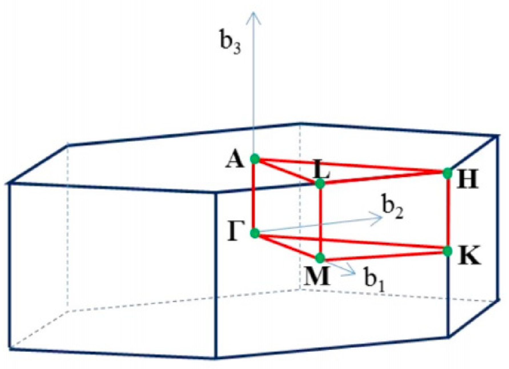
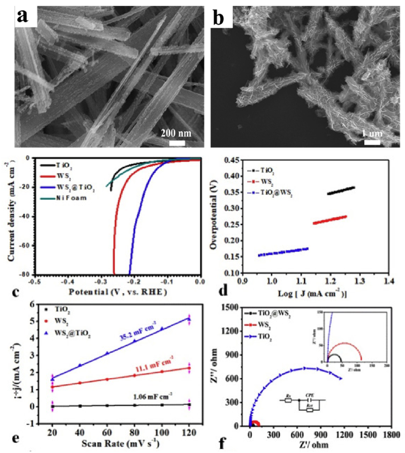
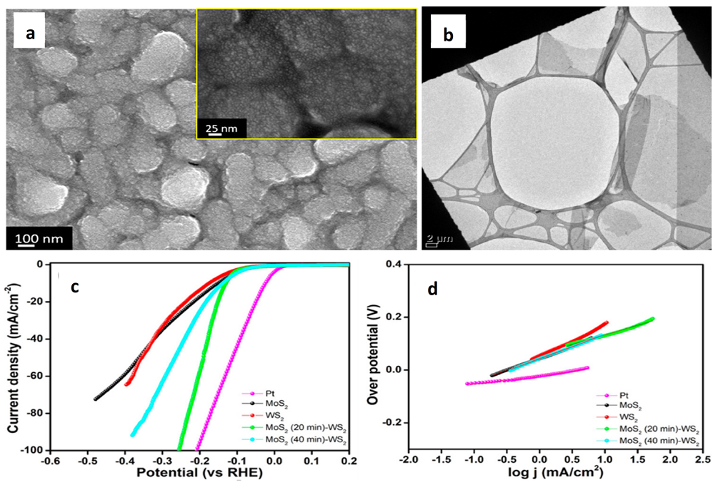
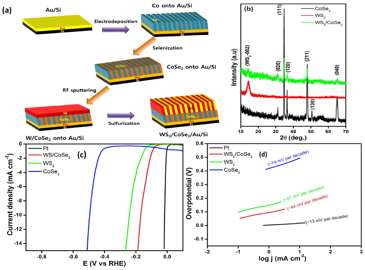
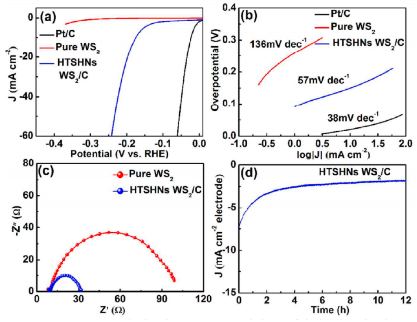
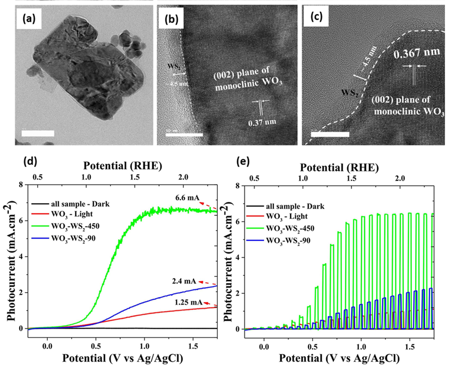
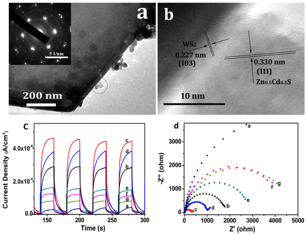
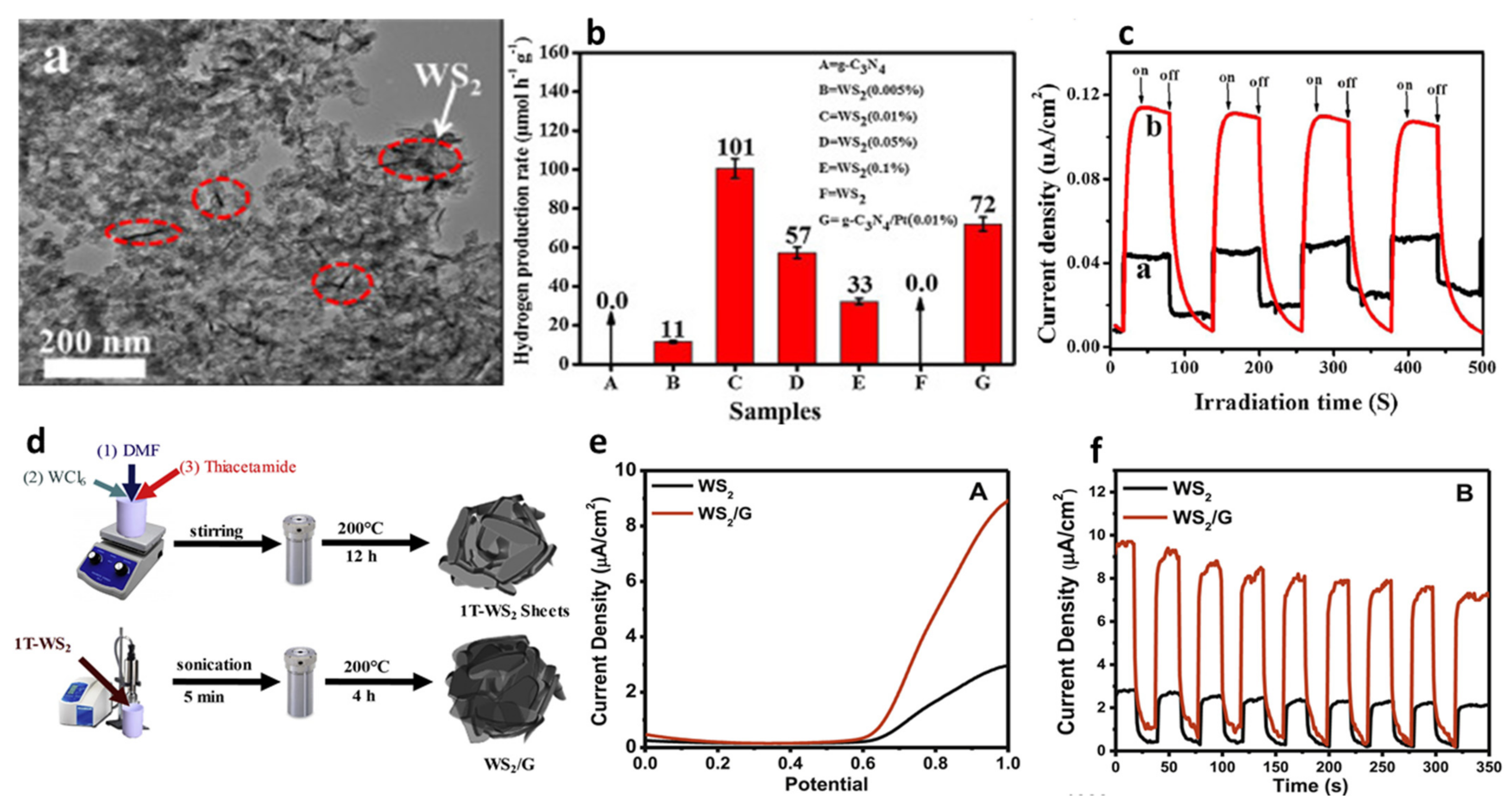
Table 1.
The HER performance of WS2 with different morphology.
| Catalyst | Substrate | Synthesis Method | Current Density mA·cm−2 | Overpotential mV | Tafel Slope mV dec−1 | Ref. |
|---|---|---|---|---|---|---|
| Layered WS2 | CC | Thermolysis | 10 | 184 | 79 | [68] |
| WS2 nanosheets | GCE | Polarization/decomposition | 10 | 157 | 60 | [69] |
| WS2 nanosheets | W foil | Anodization/sulfurization | 10 | 136 | 61 | [70] |
| WS2 film | Si/glassy carbon | Atomic layer deposition | 10 | 137 | 54 | [71] |
| WS2 nanosheets | GCE | Self-template | 10 | 145 | 67 | [72] |
| WS2 nanoribbons | Ti/Au | Chemical unzipping | 10 | 240 | 68 | [73] |
| 1T-WS2 nanobelts | GC | Electrochemical activation | 10 | 170 | 40 | [74] |
| WS2 nanosheets | CC | Hydrothermal | 10 | 116 | 37.5 | [75] |
| WS2 nanoflakes | Si | Hydrothermal | 10 | 118 | 43 | [76] |
Table 2.
Summary of the exfoliation method conditions and achieved WS2 morphology.
| Synthesis Method | Technique/Solvent/Electrolyte | Morphology | Ref. |
|---|---|---|---|
| Mechanical exfoliation | Scotch tape using Si/SiO2 wafer | Monolayers/flakes | [93] |
| Scotch tape using quartz wafer | Mono/few monolayer | [94] | |
| Chemical exfoliation | NaNO3/HCl solution | Nanosheets (4.3 nm) | [95] |
| Sodium dodecyl sulfate solution | Nanosheets | [96] | |
| Cyclohexanone/Ethyl cellulose by magnetic stirring (MS), shear mixing (SM), and horn-tip (HT) | Single/few nanosheets | [97] | |
| Aqueous ammonia | 2H nanosheets | [98] | |
| DI (deionized) water and IPA (isopropyl alcohol/vacuum filtration | Nano flakes (3.9) | ||
| Li-intercalation | Methyllithium(Me-Li), n-butyllithium (n-Bu-Li) and tert-butyllithium (t-Bu-Li) | Nano flakes | [99] |
| n-Butyllithium | 2H and 1 T nanosheets | [100] | |
| Ethylene glycol/Li hydroxide | Few layers nanosheets | [101] | |
| Electrochemical Li-intercalation | Propylene carbonate with 0.1 wt% LiClO4 | Quantum dots QD | [102] |
| A WS2 pellet, platinum mesh, and platinum wire are used as working, counter, and quasi-reference electrodes g 0.1 wt% of lithium perchlorate in deoxygenated propylene carbonate as electrolyte | Porous WS2 nanosheets | [103] | |
| Bipolar platinum electrodes, 0.5 M Na2SO4 | 1T and 2H nanosheets | [104] |
Table 3.
Examples of CVD-grown WS2 nanostructures.
| Precursors | Substrate | Growth Conditions | Morphology | Ref. |
|---|---|---|---|---|
| WO3 and elemental S powders | Si/SiO2 wafer | WO3 at 700 °C, S at 150 °C for 3 min, 380 SCCM N2, 20 sccm H2 | Nano flakes | [117] |
| WS2 and Na2S2O3 powders | Si/SiO2 wafer | 700 °C, atmospheric P, for 1 h with 30 sccm Ar/H2 (5% H2) | Leaf-like film | [118] |
| H2S and WF6 gases | Si/SiO2 wafer | 650 °C, 1 kPa with 100 sccm Ar, 15–60 min | Atomic monolayers | [119] |
| WO3 and elemental S powders | FTO/ITO | 500 °C, atmospheric gas of Ar/H2 at a pressure of about 10−2 Torr, for 3 min with 40 sccm gas flow | Nanosheets | [120] |
| WO3, elemental S and NaCl powders | Si/SiO2 wafer | 700 °C, atmospheric P for 5 min with 200 sccm Ar | Large-area monolayers | [121] |
| Tungstic acid and elemental sulfur | Si/SiO2 wafer | 900 °C, for 30 min with 50 sccm Ar flow | Nano flakes | [122] |
| WO3 and elemental S powders | c-plane sapphire | 970–1080 °C for 30 min with 500 sccm Ar flow | Bilayer nanosheets | [123] |
Table 4.
Examples of hydrothermal synthesis of WS2 nanostructures.
| Precursors | Conditions | Morphology | Application | Ref. |
|---|---|---|---|---|
| Hexaammonium heptatungstate, thiourea powders | Autoclave, titanium substrate, 200 for 7 h. | Vertical and flat 1-T nanosheets | Electrocatalytic hydrogen revolution | [76] |
| WCl6, thioacetamide powders | Autoclave, 230 for 24 h. | 1-T nanosheets | Wastewater treatment | [134] |
| WCl6, thioacetamide powders | Autoclave, 240 for 24 h under different magnetic field | 1-T nanosheets | Anode for sodium ion batteries | [135] |
| WS2 powder, NaOH solution | Autoclave, 220 for 24 h | Quantum dots | Fluorescence sensor | [136] |
| WCl6, thiourea powders | Autoclave, 180 for 48 h | Nanoplate like structure | Lithium ion battery | [137] |
| Sodium tungstate, thioacetamide | Autoclave, 200 for 24 h | Mixed phase nanosheets | Ammonia gas sensing | [138] |
Publisher’s Note: MDPI stays neutral with regard to jurisdictional claims in published maps and institutional affiliations. |
© 2021 by the authors. Licensee MDPI, Basel, Switzerland. This article is an open access article distributed under the terms and conditions of the Creative Commons Attribution (CC BY) license (https://creativecommons.org/licenses/by/4.0/).
Share and Cite
MDPI and ACS Style
Thiehmed, Z.; Shakoor, A.; Altahtamouni, T. Recent Advances in WS2 and Its Based Heterostructures for Water-Splitting Applications. Catalysts 2021, 11, 1283. https://0-doi-org.brum.beds.ac.uk/10.3390/catal11111283
AMA Style
Thiehmed Z, Shakoor A, Altahtamouni T. Recent Advances in WS2 and Its Based Heterostructures for Water-Splitting Applications. Catalysts. 2021; 11(11):1283. https://0-doi-org.brum.beds.ac.uk/10.3390/catal11111283
Chicago/Turabian StyleThiehmed, Zeineb, Abdul Shakoor, and Talal Altahtamouni. 2021. "Recent Advances in WS2 and Its Based Heterostructures for Water-Splitting Applications" Catalysts 11, no. 11: 1283. https://0-doi-org.brum.beds.ac.uk/10.3390/catal11111283
Note that from the first issue of 2016, this journal uses article numbers instead of page numbers. See further details here.