Shear Induced TiO2 Nano Structure Using Brush-Coating for Liquid Crystal Alignment

1
Department of Smart Manufacturing Engineering, Changwon National University, Gyeongnam 51140, Korea
2
Department of Electrical Engineering, Changwon National University, Gyeongnam 51140, Korea
*
Author to whom correspondence should be addressed.
Crystals 2020, 10(10), 860; https://0-doi-org.brum.beds.ac.uk/10.3390/cryst10100860
Submission received: 2 September 2020
/
Revised: 20 September 2020
/
Accepted: 22 September 2020
/
Published: 24 September 2020
(This article belongs to the Special Issue Micro and Nano Patterned Substrates for Liquid Crystal Alignment (Volume II))
Abstract
:We have developed a very useful and cost-effective liquid crystal (LC) alignment layer of brush-coated TiO2 that is solution-processable for twisted nematic (TN) LC cells. TiO2 was prepared via the sol-gel method. The TiO2 solution was brush-coated on the substrate, followed by an annealing process. During the brush-coating process, a retracting force is generated on the deposited TiO solutions along the coating direction. The annealing process hardens the TiO2 and generates shearing stress arising from the retracting force along the brush-coating direction. The shearing stress created highly oriented nano/microstructure and uniformly aligned LCs with a stable pretilt angle of 0.6°. TN mode LC cells based on brush-coated TiO2 exhibited a performance of 12.5 ms of response and a threshold voltage of 1.8 V. Our brush-coated TiO2 incorporates two steps of the film deposition and alignment process into one step.

1. Introduction
Surface engineering has contributed greatly to the development of modern technology. In particular, surface nano/micropatterning is an important technique that can improve the performance of functional devices over flat surfaces, such as optical [1,2,3], mechanical [4,5], electrical [5], and biological response [6,7,8,9], as well as increase semiconductor integration. For example, nano/microstructures, with wavy and quasi-periodicity enhance the optical properties of optics applications, including solar cells and organic light-emitting diodes [1,2,3]. In addition, because the nano/microfabrication enhances the mechanical endurance, it can make rollable and flexible electronic devices [4,5]. Moreover, surface nano/microstructures with complex geometries control the surface energy and provide desirable functionalities, such as antimicrobial properties, biocompatibility, and environmental responsiveness of the surface [6,7,8,9].
In addition, the solution coating process is also an important technique for enhancing the performance of functional devices, because it is directly connected to the quality of the film, such as orientation and crystallization, which affects the performance of the devices. [10,11]. Various solution processes, including spin-coating [12], dip-coating [13], blade coating [14], and brush-coating [15,16], have been developed for advanced performance of the devices. For example, the desirable performance of optics and electronics devices can be achieved by producing high-quality polymer films or quantum dot deposition by adopting various solution coating techniques [17,18,19]. Among the several solution coating techniques, brush-coating allows controllable liquid transfer by shearing the solution and successfully orienting the materials, which can obtain a higher performance of opto-electrical devices [15,16]. Therefore, the brush-coating can be useful when the materials require an oriented nano/microstructure.
Liquid crystal (LC)-based devices are very suitable for adopting brush-coatings because they require an oriented structure. LC devices can be successfully operated under the condition of uniform LC alignment, which is the core technology for uniform and high quality electro-optical performance [20]. Various alignment techniques, including the rubbing process [21], ultraviolet photo-alignment technique [22], nanoimprint lithography [23], and ion beam irradiation [24], have been developed for uniform LC alignment. Although these methods have several advantages, such as high quality and desirable performance, these techniques suffer from limitations, such as the generation of contaminant debris and the limitation of a large-area process with high cost. Thus, a need to develop alignment technique for advanced LC devices arises.
Herein, we incorporated the film deposition process and alignment techniques within one step by adopting a brush-coating. As mentioned previously, LC device fabrication should be accompanied by an alignment technique after the alignment layer deposition. Since brush-coating can deposit a film with an oriented structure, the fabrication process of the LC device can be reduced to one step, with high throughput and cost effectiveness. We propose that the brush-coating can direct the orientation of the surface by shearing stress and construct the nano/microstructure on the surface, which can align uniformly the LC molecules. Titanium oxide (TiO2) was used as the alignment layer that was prepared by a sol-gel process. TiO2 has been investigated for photocatalysis on optical devices with low cost, nontoxicity, and high chemical stability [25,26]. The LC alignment state was observed by cross-polarized optical microscopy (POM) with a pre-tilt angle. Atomic force microscopy (AFM) was used to verify the effect of the brush-coating on aligning the LC molecules as compared with the spin-coating process not accompanied by an alignment technique. X-ray photoelectron spectroscopy (XPS) was used to confirm the chemical structure of TiO2. Finally, the electro-optical (EO) property of a twisted nematic (TN) cell was measured with the response time (RT) and voltage–transmittance (V–T).
2. Materials and Methods
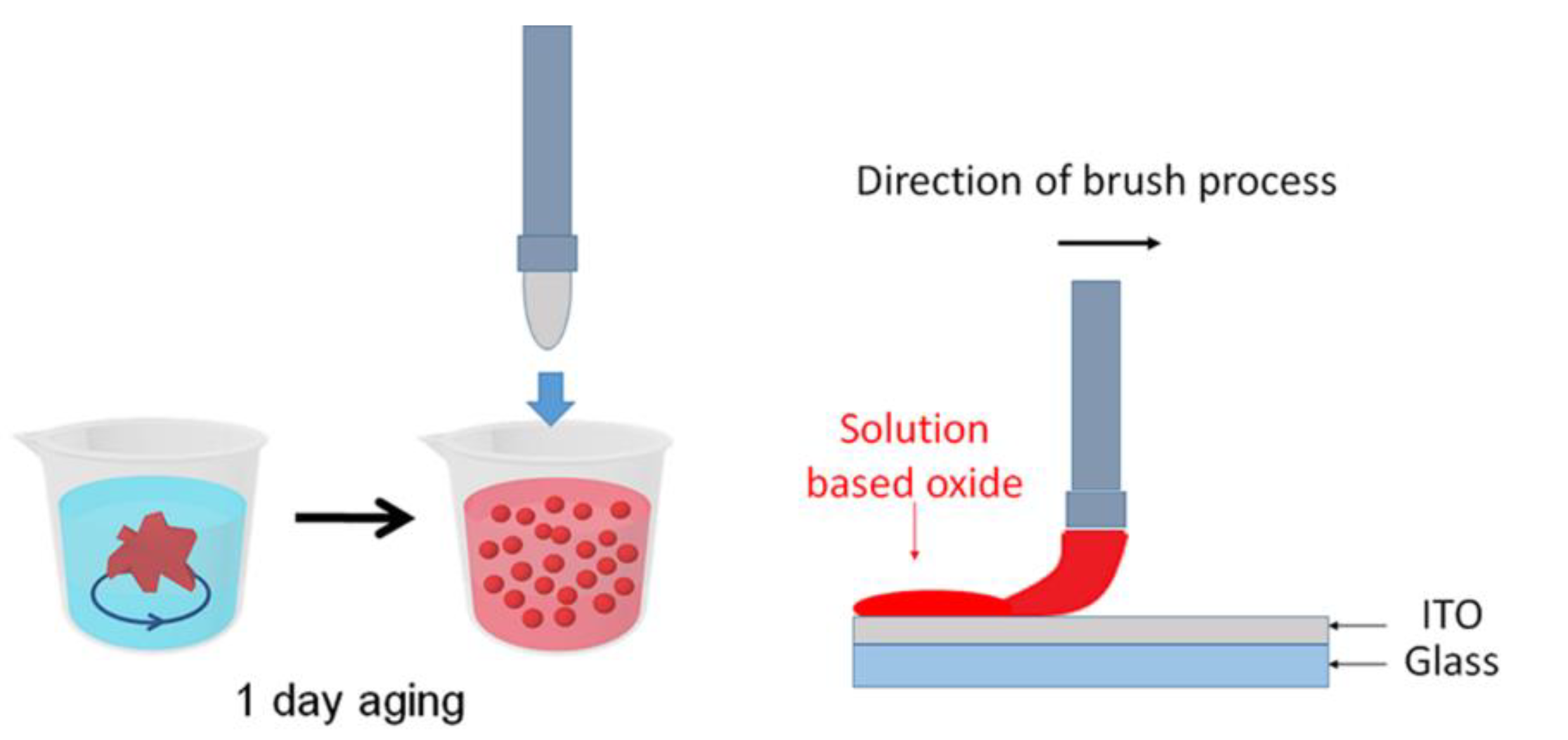
The TiO2 film was prepared using a brush-coating process on indium tin oxide (ITO)-coated glass substrates (Samsung Corning 1737: standard 32 × 22 × 1.1 mm3, sheet resistance: 10 Ω sq−1). Prior to deposition, the TiO2 solution was prepared by a sol-gel process, and the ITO-coated glass substrates were cleaned by ultrasonication in acetone, methanol, and deionized water for 10 min and dried with N2 gas. Titanium (IV) isopropoxide (Ti[OCH(CH3)2]4 (Mw = 284.22 g/mol) was used as the titanium precursor and was dissolved in 2-methoxyethanol (2 ME). Acetic acid was dropped into a solution as a stabilizer. The solutions were stirred at 45 °C for 1 h at 600 rpm and were allowed to age for 1 day. Figure 1 illustrates the brush-coating process with the solution as an ink, which is prepared by a sol-gel process. The prepared solution was brush-coated onto ITO-coated glass substrates, followed by pre-baking on a hot plate at 100 °C for 10 min. The samples were then annealed in a furnace at 160 °C for 1 h. LC cells with an anti-parallel configuration were fabricated with a cell gap of 60 μm to confirm the LC alignment properties using polarized optical microscopy (POM) (BXP51, Olympus, Japan) images and pre-tilt angles. TN cells were also fabricated to measure the electro-optical properties of RT and V–T with a 5 μm-wide cell gap. To assemble the TN cell using a brush-coating process, TiO2 was brush-coated perpendicularly on the bottom and the upper ITO-coated glass substrates, which indicated that the brush-coating direction of one substrate was perpendicular to that of the other substrate. The empty cells were filled with positive nematic LCs (MJ001929; ne = 1.5859, no = 1.4872, and △ε = 8.2; Merck) via capillary action in the isotropic phase. POM was used to verify the LC alignment state, and the pre-tilt angles were measured using a modified crystal rotation method (TBA 107, Autronic). The EO characteristics of V–T and RT were measured using an LCD evaluation system (LCMS-200, Sesim). Atomic force microscopy (AFM; XE-100, Park System, Korea) was used to measure the surface properties of the TiO2 film compared with the brush-coating and spin-coating. The optical transmittance was measured in the range 250–800 nm at room temperature of 25 °C using an ultraviolet—visible (UV–Vis) spectrophotometer (V-650, JASCO Corporation, Japan).
3. Results & Discussion
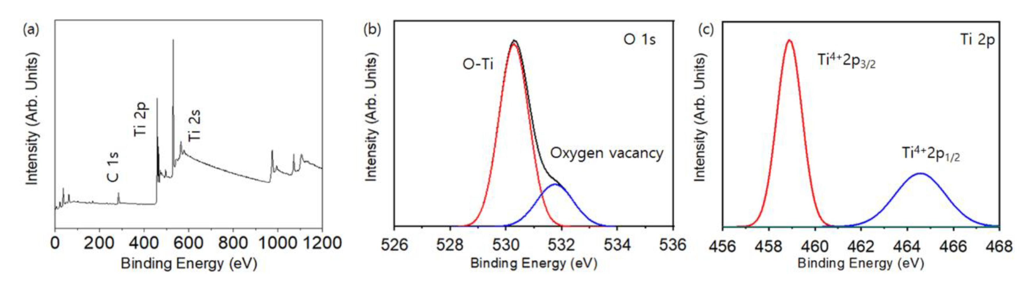
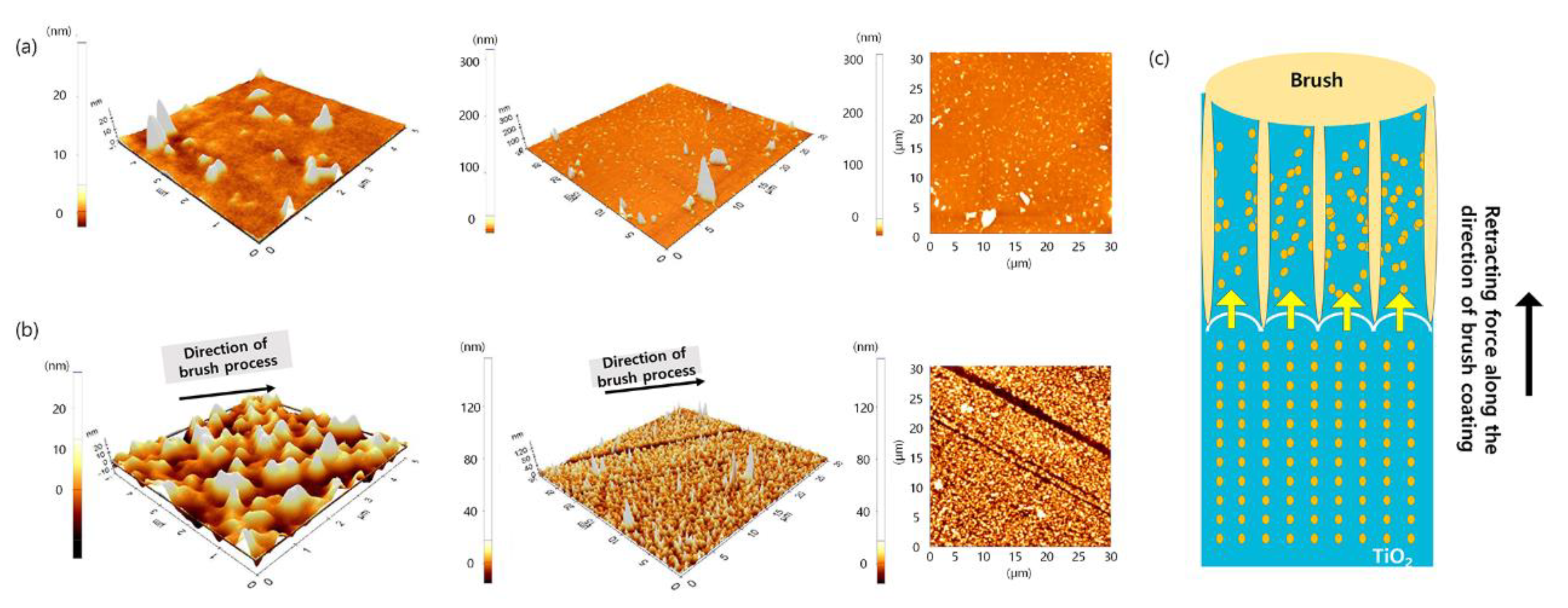
Chemical analysis was conducted to verify that TiO2 was properly deposited by brush-coating. The XPS spectra of the TiOx samples are presented in Figure 2. The Ti and O elements were confirmed in the wide-scan XPS spectrum, as shown in Figure 2a. The bonding energy around 460 eV represents the Ti 2p peak and that around 532 eV indicates the O 1s peak. All binding energies were referenced to the C1s signal at 284.6 eV. The XPS spectra of Ti 2p were deconvoluted using a Gaussian filter. The spectra consist of Ti 2p3/2 and Ti 2p1/2 spin-orbit doublets with peaks located at 458.9 eV and 464.5 eV, respectively. In addition, the spin-orbit parameter of 5.8 eV was typically attributed to the Ti4+ oxidation state as the TiO2 lattice. These peaks are consistent with the pure TiO2 spectrum [27]. The O 1s spectra consisted of two components with oxygen in TiO2 lattices centered at 530 eV, and oxygen vacancies centered at 532 eV. The portion of oxygen in the lattice of 77% is much higher than the oxygen vacancies of 23%, which is similar to the pure TiO2 composition [28]. These results indicate that the brush-coating forms TiO2 film properly and show a stoichiometric structure. Figure 3 shows the three-dimensional and surface AFM topographies of the TiO2 along the deposition process of spin-coated TiO2 (Figure 3a) and brush-coated TiO2 (Figure 3b). The spin-coated TiO2 presents an entirely flat surface with a small number of large particles, which might be the debris and cannot determine the surface anisotropy. A root mean square (RMS) of 2.267 nm was obtained for the spin-coated TiO2 (Table 1). The spin-coating process spun the TiO2 solution at high speeds and generated a centrifugal force on the surface, which induced a smooth surface without anisotropy on the surface. By contrast, the brush-coated TiO2 shows a uniform but relatively rough surface with a slightly larger RMS roughness of 6.318 nm than that of the spin-coating process (Table 1). In addition, it shows a nano/micropattern along the direction of the brush-coating (the black arrow in the AFM images). During the brush-coating, receding a brush along the direction of the coating induces the retracting force on the deposited bulk of the solution, which is attributed to the controllable liquid transfer. The subsequent annealing process solidifies the solutions into the film with shearing stress arising from the retracting forces. Therefore, receding a brush generates a shearing stress on the sol state of TiO2, and the oriented TiO2 nano/mico structure can be obtained after the annealing process.
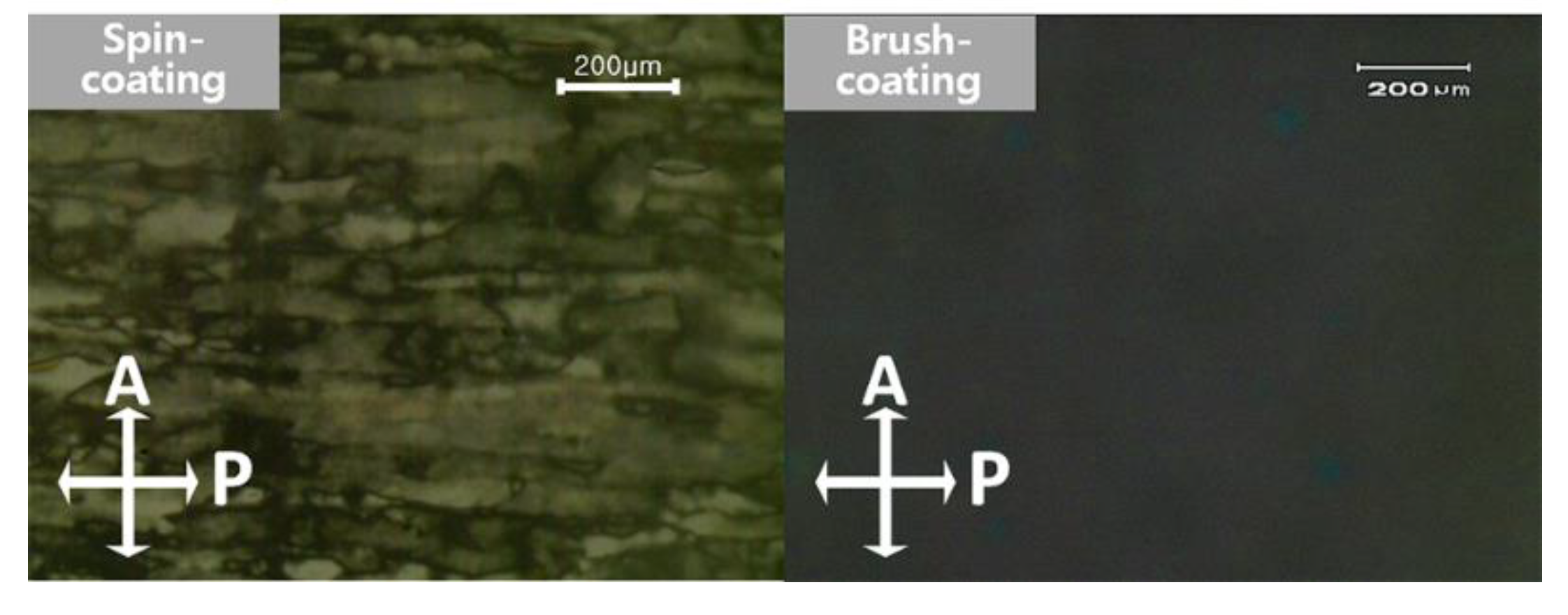
The quality of LC devices is determined by the LC alignment property. Figure 4 shows photomicrographs of the anti-parallel LC cells based on the TiO2 films fabricated by the brush-coating and spin-coating process without any alignment techniques. A black POM image was observed on the LC cell with the brush-coating process. The black image indicates that the LC molecules were uniformly aligned in one direction without any dislocation. Because the LC cell is placed between the intersectional polarizers, the polarized light from the bottom directly propagates through stably aligned LC molecules without scattering and blocks the upper crossed polarizer. Because the LCs are characterized by their collective behavior with fluidity, due to the van der Waals forces among LC molecules, they are accompanied by elastic distortion, which can be controlled by the boundary conditions, especially surface anisotropy such as microgrooves. Brush-coating creates highly oriented nano/microstructure along the direction of brush-coating due to brush retraction [15]. The anisotropic surface pattern created by the brush-coating induces geometric restrictions at the boundary condition of the interface between the LCs and TiO2 surface and controls the directional behavior of the LCs along the direction of the brush-coating. Stably oriented LCs at the interface maintain their direction and propagate their directional characteristics through the bulk state of LCs by collective behavior. On the other hand, the LC cells based on the spin-coated TiO2 showed uneven transmittance of the POM images. The spin-coated TiO2 cannot provide the director on the LC matrix. Thus, the LCs are randomly distributed on the spin-coated TiO2 without any anisotropy on the surface. Because the LCs were not uniformly aligned on the spin-coated TiO2, the light from the bottom was scattered during the propagation through the randomly distributed LC matrix and uneven transmittance of the POM images was shown.
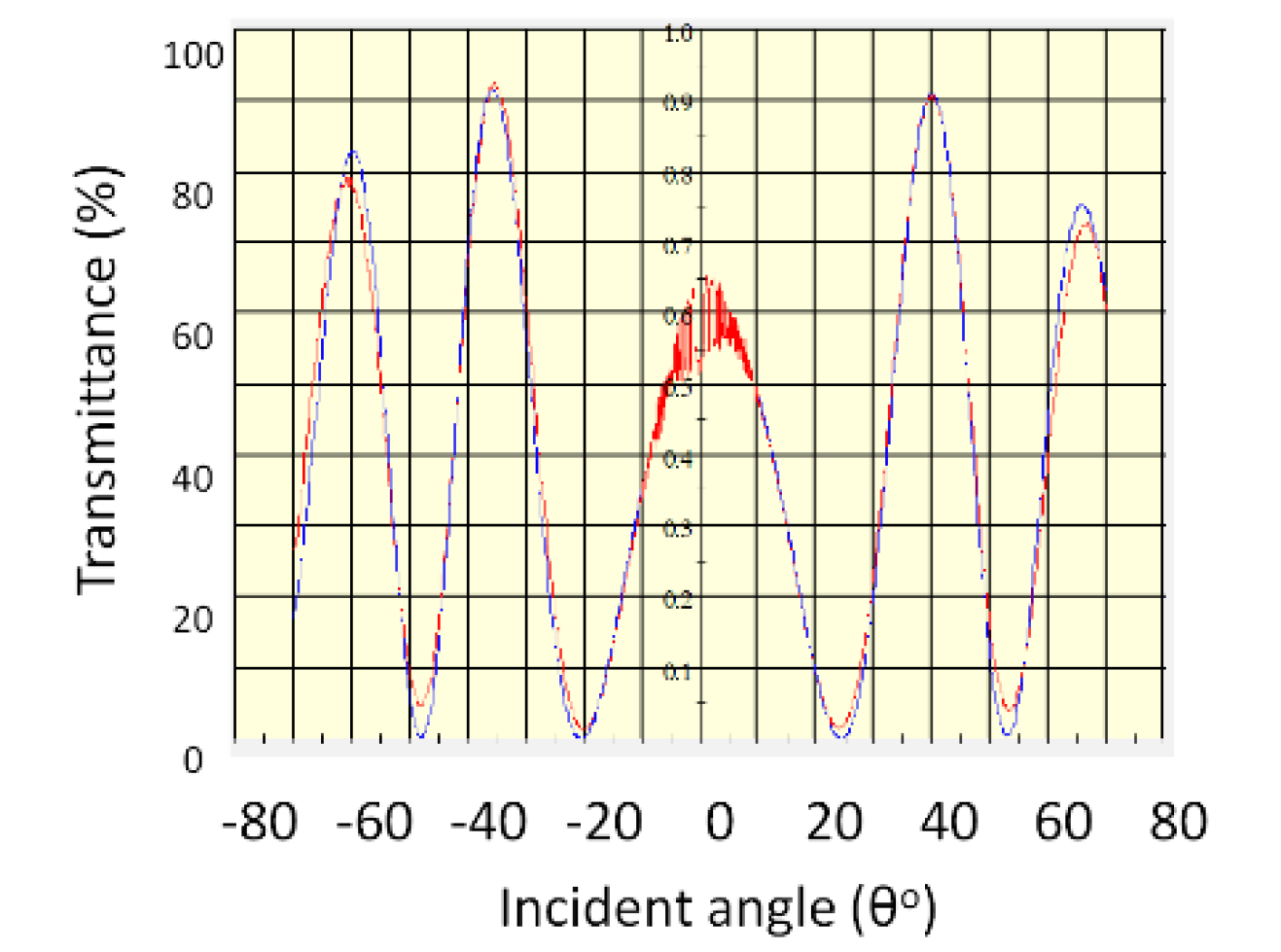
The pretilt angles of the LC cells were measured using the crystal rotation method. The crystal rotation method measures the transmittance by rotating the LC cell latitudinally by 70°, as shown in Figure 5. The blue line shows the simulated curves, and the red line shows the experimental curves measured by the LC cell. Two identical curves indicate the uniform alignment of LCs. The calculated pretilt angle by the crystal rotation method using phase retardation was measured to be 0.6°. The homogeneous LC alignment was observed on the brush-coated TiO2.
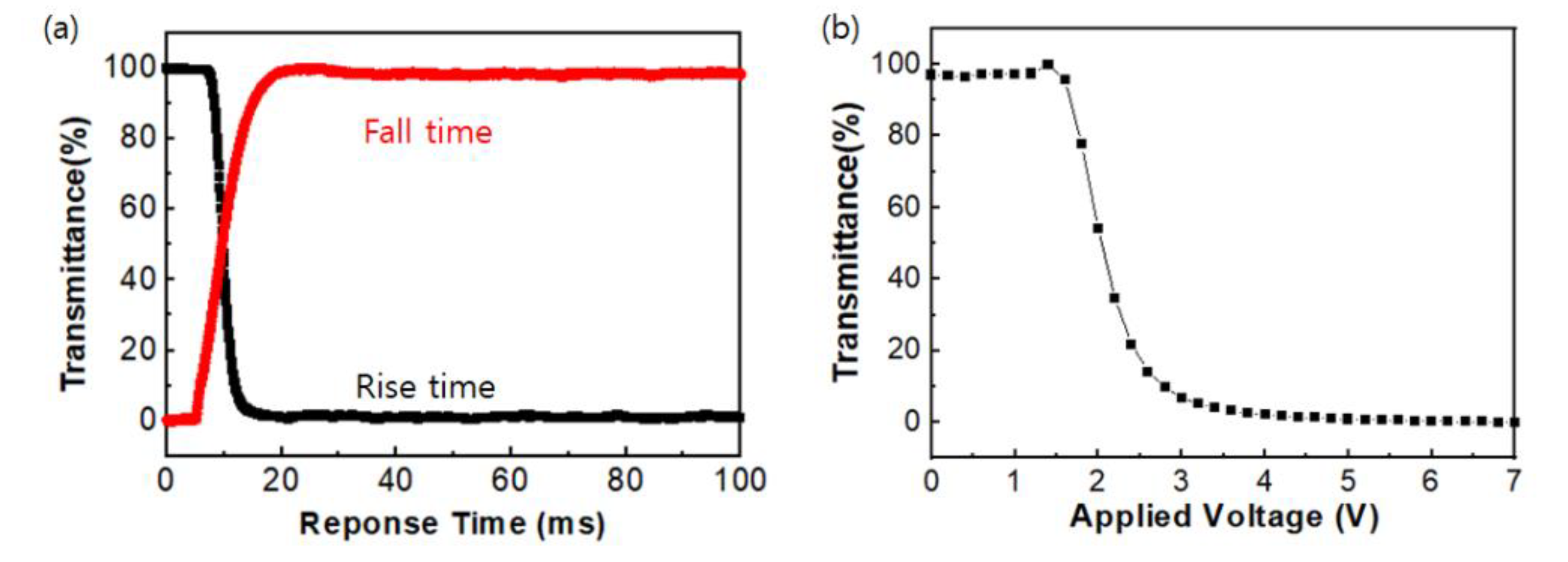
Figure 6 shows the EO characteristics of RT and VT of TN cells on the brush-coated TiO2 films measured to examine the LC applications. The light from the backlight was transmitted through the TN cells without voltage bias (0 V) due to the LC matrix twisted along the brush direction, and it propagates along the twisted configuration of the LCs (transmittance of 100%). By contrast, the light is completely blocked (transmittance of 0%) under an applied voltage (5 V) because the positive LCs were upright along the electric fields. The RT characteristics of TN cells on brush-coated TiO2 films were measured to be 3.7 ms of rise time (from 0 V to 5 V) and 9.1 ms of fall time (from 5 V to 0 V). The threshold voltage, which is the applied voltage at 90% transmission, was measured to be 1.8 V, which is similar to that of a conventional TN cell with a rubbed PI of approximately 2.0 V [29]. The TN cell based on the brush-coated TiO2 is well-operated and the TiO2 prepared by brush-coating is appropriate for the LC devices, even though it reduces the additional process for alignment.
4. Conclusions
Herein, we successfully demonstrated the use of brush-coated TiO2 as an alignment layer for LC devices. The brush-coating is a very useful and cost-effective process because it incorporates the two steps of deposition of the alignment layer and alignment process to obtain anisotropic characteristics on the surface in one step. The brush-coating creates a stoichiometric structure of TiO2, which was confirmed by XPS analysis. From the surface morphology analysis using AFM, the brush-coating creates a highly oriented nano/microstructure along the direction of the brush-coating due to shear stress arising from the brush retraction. Since the LCs are characterized by fluid-elastic properties, due to their collective behavior, the oriented nano/microstructure induces the surface anisotropy and geometric restriction on LCs; stably oriented LCs can be obtained by brush-coating, which confirms the evaluation of alignment properties using POM analysis. By contrast, the spin-coated TiO2 cannot provide the director on the surface; the LCs were not aligned in the uni-direction. The pre-tilt angle of the brush-coated TiO2 film was measured to confirm the uniform and homogenous LC alignment state. The LC cell in TN mode showed a successful operation of 12.5 ms of response time (4.2 ms of rise time and 8.3 ms of fall time) and of threshold voltage of 1.8 V. Compared with TN mode LC cell based on conventional rubbed PI, we can confirm that significant performance of TN mode based on brush-coated TiO2 was obtained with reducing one step process. Our brush-coated TiO2 has great potential and is useful for the fabrication of LC devices.
Author Contributions
Conceptualization, H.-C.J.; formal analysis, J.I.J. and H.-C.J.; investigation, J.I.J.; data curation, J.I.J. and H.-C.J.; writing—original draft preparation, J.I.J. and H.-C.J.; writing—review and editing, J.I.J. and H.-C.J.; visualization, J.I.J. and H.-C.J.; supervision, H.-C.J.; project administration, H.-C.J.; funding acquisition, H.-C.J. All authors have read and agreed to the published version of the manuscript.
Funding
This research was funded by Changwon National University in 2019–2020.
Conflicts of Interest
The authors declare no conflict of interest.
References
- Fan, P.; Yu, Z.; Fan, S.; Brongersma, M.L. Optical Fano resonance of an individual semiconductor nanostructure. Nat. Mater. 2014, 13, 471–475. [Google Scholar] [CrossRef] [PubMed]
- Koo, W.H.; Jeong, S.M.; Araoka, F.; Ishikawa, K.; Nishimura, S.; Toyooka, T.; Takezoe, H. Light extraction from organic light-emitting diodes enhanced by spontaneously formed buckles. Nat. Photonics 2010, 4, 222–226. [Google Scholar] [CrossRef]
- Lee, W.-K.; Yu, S.; Engel, C.J.; Reese, T.; Rhee, D.; Chen, W.; Odom, T.W. Concurrent design of quasi-random photonic nanostructures. Proc. Natl. Acad. Sci. USA 2017, 114, 8734–8739. [Google Scholar] [CrossRef] [PubMed] [Green Version]
- Gao, L.; Zhang, Y.; Zhang, H.; Doshay, S.; Xie, X.; Luo, H.; Shah, D.; Shi, Y.; Xu, S.; Fang, H.; et al. Optics and nonlinear buckling mechanics in large-area, highly stretchable arrays of plasmonic nanostructures. ACS Nano 2015, 9, 5968–5975. [Google Scholar] [CrossRef] [PubMed]
- Khang, D.Y.; Jiang, H.; Huang, Y.; Rogers, J.A. A stretchable form of single-crystal silicon for highperformance electronics on rubber substrates. Science 2006, 311, 208–212. [Google Scholar] [CrossRef] [Green Version]
- Kim, D.-H.; Ghaffari, R.; Lu, N.; Rogers, J.A. Flexible and stretchable electronics for biointegrated devices. Annu. Rev. Biomed. Eng. 2012, 14, 113–128. [Google Scholar] [CrossRef] [Green Version]
- Chen, B.; Frank-Finney, R.J.; Gupta, M. Fabricating Polymer Canopies onto Structured Surfaces Using Liquid Scaffolds. ACS Appl. Mater. Interfaces 2015, 7, 23056–23061. [Google Scholar] [CrossRef] [PubMed]
- Fuchs, A.D.; Tiller, J.C. Contact-Active Antimicrobial Coatings Derived from Aqueous Suspensions. Angew. Chem. Int. Ed. 2006, 45, 6759–6762. [Google Scholar] [CrossRef]
- Wu, Z.; Tong, W.; Jiang, W.; Liu, X.; Wang, Y.; Chen, H. Poly(Nvinylpyrrolidone)-Modified Poly(dimethylsiloxane) Elastomers As Anti-Biofouling Materials. Colloids Surf. B 2012, 96, 37–43. [Google Scholar] [CrossRef] [PubMed]
- Ren, Z.J.; Zhang, X.; Li, H.H.; Sun, X.L.; Yan, S.K. A Facile Way to Fabricate Anisotropic P3ht Films by Combining Epitaxy and Electrochemical Deposition. Chem. Commun. 2016, 52, 10972–10975. [Google Scholar] [CrossRef] [PubMed]
- Sun, D.M.; Li, Y.X.; Ren, Z.J.; Bryce, M.R.; Li, H.H.; Yan, S.K. Anisotropic Highly-Conductive Films of Poly(3-Methylthiophene) from Epitaxial Electropolymerization on Oriented Poly(Vinylidene Fluoride). Chem. Sci. 2014, 5, 3240–3245. [Google Scholar]
- Schmidt, S.; Motschmann, H.; Hellweg, T.; von Klitzing, R. Thermoresponsive Surfaces by Spin-Coating of PNIPAM-co-PAA Microgels: A Combined AFM and Ellipsometry Study. Polymer 2008, 49, 749–756. [Google Scholar]
- Li, L.; Gao, P.; Baumgarten, M.; Mullen, K.; Lu, N.; Fuchs, H.; Chi, L. High Performance Field-Effect Ammonia Sensors Based on a Structured Ultrathin Organic Semiconductor Film. Adv. Mater. 2013, 25, 3419–3425. [Google Scholar]
- Wu, X.; Lan, S.; Zhang, G.; Chen, Q.; Chen, H.; Guo, T. Morphology of a Ternary Blend Solar Cell Based on Small Molecule: Conjugated Polymer: Fullerene Fabricated by Blade Coating. Adv. Funct. Mater. 2017, 27, 1703268. [Google Scholar]
- Zhang, M.; Hu, B.; Meng, L.; Bian, R.; Wang, S.; Wang, Y.; Liu, H.; Jiang, L. Ultrasmooth Quantum Dot Micropatterns by a Facile Controllable Liquid-Transfer Approach: Low-Cost Fabrication of HighPerformance QLED. J. Am. Chem. Soc. 2018, 140, 8690–8695. [Google Scholar] [PubMed]
- Guo, C.; Gao, X.; Lin, F.-J.; Wang, Q.; Meng, L.; Bian, R.; Sun, Y.; Jiang, L.; Liu, H. In Situ Characterization of the Triphase Contact Line in a BrushCoating Process: Toward the Enhanced Efficiency of Polymer Solar Cells. ACS Appl. Mater. Interfaces 2018, 10, 39448–39454. [Google Scholar] [PubMed]
- Kwak, J.; Bae, W.K.; Lee, D.; Park, I.; Lim, J.; Park, M.; Cho, H.; Woo, H.; Yoon, D.Y.; Char, K.; et al. Bright and efficient full-color colloidal quantum dot light-emitting diodes using an inverted device structure. Nano Lett. 2012, 12, 2362–2366. [Google Scholar]
- Jiang, C.; Zhong, Z.; Liu, B.; He, Z.; Zou, J.; Wang, L.; Wang, J.; Peng, J.; Cao, Y. Coffee-ring-free quantum dot thin film using inkjet printing from a mixed-solvent system on modified ZnO transport layer for light-emitting devices. ACS Appl. Mater. Interfaces 2016, 8, 26162–26168. [Google Scholar]
- Zhu, T.; Shanmugasundaram, K.; Price, S.C.; Ruzyllo, J.; Zhang, F.; Xu, J.; Mohney, S.E.; Zhang, Q.; Wang, A.Y. Mist fabrication of light emitting diodes with colloidal nanocrystal quantum dots. Appl. Phys. Lett. 2008, 92, 023111. [Google Scholar]
- Palermo, G.; Cataldi, U.; Sio, L.; Burgi, T.; Tabiryan, N.; Umeton, C. Optical control of plasmonic heating effects using reversible photo-alignment of nematic liquid crystals. Appl. Phys. Lett. 2016, 109, 191906. [Google Scholar]
- Ho, J.Y.L.; Chigrinov, V.G.; Kwok, H.S. Variable liquid crystal pretilt angles generated by photoalignment of a mixed polyimide alignment layer. Appl. Phys. Lett. 2007, 90, 243506. [Google Scholar] [CrossRef] [Green Version]
- Hsu, C.-J.; Chen, B.-L.; Huang, C.-Y. Controlling liquid crystal pretilt angle with photocurable prepolymer and vertically aligned substrate. Opt. Express 2016, 24, 1463–1471. [Google Scholar] [CrossRef]
- Jeong, H.-C.; Lee, J.H.; Won, J.; Oh, B.Y.; Kim, D.H.; Lee, D.W.; Song, I.H.; Liu, Y.; Seo, D.-S. One-dimensional surface wrinkling for twisted nematic liquid crystal display based on ultraviolet nanoimprint lithography. Opt. Express 2019, 27, 18094. [Google Scholar] [CrossRef] [PubMed]
- Jeong, H.-C.; Lee, J.H.; Kim, D.H.; Lee, D.W.; Han, J.M.; Oh, B.-Y.; Kim, T.W.; Seo, D.-S. Liquid crystal alignment on ionbeam irradiated bismuth-doped tin oxide films and their application to liquid crystal displays. Liq. Cryst. 2019, 46, 86–93. [Google Scholar] [CrossRef]
- Kartikay, P.; Nemala, S.S.; Mallick, S. One-dimensional TiO2 nanostructured photoanode for dyesensitized solar cells by hydrothermal synthesis. J. Mater. Sci. Mater. Electron. 2017, 28, 11528–11533. [Google Scholar] [CrossRef]
- Bharti, B.; Kumar, S.; Lee, H.-N.; Kumar, R. Formation of oxygen vacancies and Ti3+ state in TiO2 thin film and enhanced optical properties by air plasma treatment. Sci. Rep. 2016, 6, 32355. [Google Scholar] [CrossRef]
- Meng, A.; Zhang, L.; Cheng, B.; Yu, J. Dual Cocatalysts in TiO2 Photocatalysis. Adv. Mater. 2019, 31, 1807660. [Google Scholar] [CrossRef]
- Wang, L.; Qi, T.; Wang, J.; Zhang, S.; Xiao, H.; Ma, Y. Uniform dispersion of cobalt nanoparticles over nonporous TiO2 with low activation energy for magnesium sulfate recovery in a novel magnesia-based desulfurization process. J. Hazard. Mater. 2018, 342, 579–588. [Google Scholar] [CrossRef]
- Lee, Y.-G.; Park, H.-G.; Jeong, H.-C.; Lee, J.H.; Heo, G.-S.; Seo, D.-S. Homogeneous liquid crystal alignment characteristics on solution-derived HfYGaO films treated with IB irradiation. Opt. Express 2015, 23, 17291. [Google Scholar] [CrossRef]
Figure 1.
Schematic of the fabrication procedure for brush-coating process using TiO2 solution obtained from sol-gel method as an alignment layer for liquid crystal device.
Figure 1.
Schematic of the fabrication procedure for brush-coating process using TiO2 solution obtained from sol-gel method as an alignment layer for liquid crystal device.

Figure 2.
(a) Wide scan image, (b) O 1s and (c) Ti 2p core level X-ray photoelectron spectroscopy spectra of brush-coated TiO2.
Figure 2.
(a) Wide scan image, (b) O 1s and (c) Ti 2p core level X-ray photoelectron spectroscopy spectra of brush-coated TiO2.

Figure 3.
3-D Atomic force microscopy images and surface morphologies for (a) spin-coated TiO2 and (b) brush-coated TiO2. (c) Schematic of brush-coating induced TiO2 alignment by brush retraction.
Figure 3.
3-D Atomic force microscopy images and surface morphologies for (a) spin-coated TiO2 and (b) brush-coated TiO2. (c) Schematic of brush-coating induced TiO2 alignment by brush retraction.

Figure 4.
Polarized optical microscopy images of liquid crystals cell consist of TiO2 deposited by spin-coating and brush-coating.
Figure 4.
Polarized optical microscopy images of liquid crystals cell consist of TiO2 deposited by spin-coating and brush-coating.

Figure 5.
Transmittance versus incident angle for the LC cell based on the brush-coated TiO2 measured by crystal rotation method.
Figure 5.
Transmittance versus incident angle for the LC cell based on the brush-coated TiO2 measured by crystal rotation method.

Figure 6.
Electro-optical characteristics of TN mode based on the brush-coated TiO2 (a) response time (b) voltage-transmittance.
Figure 6.
Electro-optical characteristics of TN mode based on the brush-coated TiO2 (a) response time (b) voltage-transmittance.


Table 1.
Surface roughness of spin-coated and brush-coated TiO2.
| Title | Surface Roughness (nm) |
|---|---|
| Spin-coated TiO2 | 2.267 |
| Brush-coated TiO2 | 6.318 |
© 2020 by the authors. Licensee MDPI, Basel, Switzerland. This article is an open access article distributed under the terms and conditions of the Creative Commons Attribution (CC BY) license (http://creativecommons.org/licenses/by/4.0/).
Share and Cite
MDPI and ACS Style
Jang, J.I.; Jeong, H.-C. Shear Induced TiO2 Nano Structure Using Brush-Coating for Liquid Crystal Alignment. Crystals 2020, 10, 860. https://0-doi-org.brum.beds.ac.uk/10.3390/cryst10100860
AMA Style
Jang JI, Jeong H-C. Shear Induced TiO2 Nano Structure Using Brush-Coating for Liquid Crystal Alignment. Crystals. 2020; 10(10):860. https://0-doi-org.brum.beds.ac.uk/10.3390/cryst10100860
Chicago/Turabian StyleJang, Jong In, and Hae-Chang Jeong. 2020. "Shear Induced TiO2 Nano Structure Using Brush-Coating for Liquid Crystal Alignment" Crystals 10, no. 10: 860. https://0-doi-org.brum.beds.ac.uk/10.3390/cryst10100860
Note that from the first issue of 2016, this journal uses article numbers instead of page numbers. See further details here.