Improvement on Thermal Stability of Nano-Domains in Lithium Niobate Thin Films


The MOE Key Laboratory of Weak-Light Nonlinear Photonics, School of Physics and TEDA Applied Physics Institute, Nankai University, Tianjin 300457, China
*
Author to whom correspondence should be addressed.
Crystals 2020, 10(2), 74; https://0-doi-org.brum.beds.ac.uk/10.3390/cryst10020074
Submission received: 23 December 2019
/
Revised: 17 January 2020
/
Accepted: 22 January 2020
/
Published: 30 January 2020
(This article belongs to the Special Issue Recent Progress in Lithium Niobate)
Abstract
:We present a simple and effective way to improve the thermal stability of nano-domains written with an atomic force microscope (AFM)-tip voltage in a lithium niobate film on insulator (LNOI). We show that nano-domains in LNOI (whether in the form of stripe domains or dot domains) degraded, or even disappeared, after a post-poling thermal annealing treatment at a temperature on the order of ∼100 C. We experimentally confirmed that the thermal stability of nano-domains in LNOI is greatly improved if a pre-heat treatment is carried out for LNOI before the nano-domains are written. This thermal stability improvement of nano-domains is mainly attributed to the generation of a compensating space charge field parallel to the spontaneous polarization of written nano-domains during the pre-heat treatment process.
1. Introduction
Lithium niobate (LiNbO), one of the most versatile ferroelectric materials, has been widely studied due to its excellent performance on electro-optic modulation [1,2], acousto-optic modulation [3] and nonlinear optics [4,5]. Recently, the technique of lithium niobate film on insulators (LNOI) [6,7,8] has attracted much attention for its potential applications in integrated devices. Numerous novel optical elements based on LNOI have been reported, including photonic crystals [9], high-Q microresonators [10], ridge waveguides [11], and hybrid lightwave circuits [12].
By applying a polarization reversal voltage, via an atomic force microscope (AFM)-tip, domain reversal and domain patterning can be realized in lithium niobate thin films. Based on this technique, Gainutdinov et al. [13] reported that the size and shape of domain patterns can be precisely controlled, enabling the realization of periodically poled lithium niobate (PPLN) with period of hundreds of nanometers. PPLN films can be used for quasi-phase-matching (QPM) devices, such as PPLN microcavities [14] and PPLN waveguides [15], to achieve frequency conversion. Obviously, the stability of written domains is very important for LNOI-based applications such as PPLN microcavities, PPLN waveguides, and nonvolatile ferroelectric domain memories [16,17,18,19].
Several groups have studied the thermal stability of domains in various ferroelectric materials, such as Rb-doped KTiOPO [20], LiTaO [21], Pb(ZrTi)O [22], and LiNbO [23,24]. They reported that the ferroelectric domains would degrade, or even disappear, after heat treatment. Moreover, Shao et al. [25] reported that the domain structures fabricated on LNOI are unstable even at room temperature. Obviously, such instability would prevent the ferroelectric domains from applications where the device temperature will rise due to light absorption or due to high temperature environments.
In this paper, we propose a simple and effective method to improve the thermal stability of nano-domains in lithium niobate thin films. We confirmed that nano-domains written in LNOI by applying an AFM-tip voltage were unstable at high temperatures in the order of ∼100 C. However, we found that the domain stability can be significantly improved if the LNOI sample experiences a pre-heat treatment before the nano-domain fabrication process. The underlying mechanism was also discussed.
2. Materials and Methods
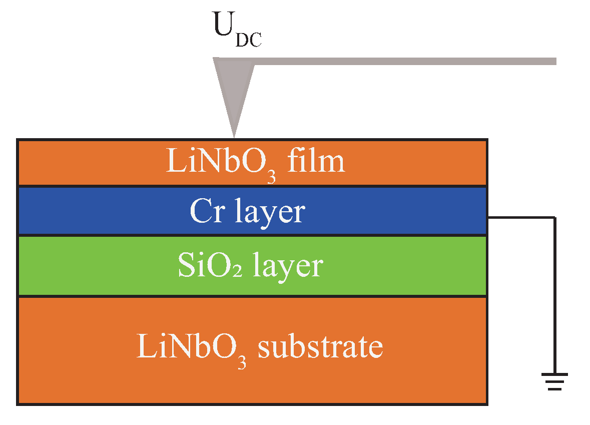
The schematic experimental setup is shown in Figure 1, in which the structure of the LNOI sample used in our experiments is also clearly shown. The LNOI sample was composed of a 300-nm thick +Z-cut ion-sliced LiNbO thin film, a 100-nm thick Cr thin film, a 2-m thick SiO layer, and a 500-m thick LiNbO substrate, which were all layered or bonded to one another in sequence. The 100-nm thick Cr layer served as a bottom electrode when an AFM-tip voltage was applied on the top 300-nm thick LiNbO thin film. Here, different metals may be used as the bottom electrode and different metal-lithium-niobate interfaces may have an effect on the domain poling process, but this is not the main topic of the current paper and will not be explored here.
In the experiments, the top LiNbO film was poled directly by applying a DC voltage through an AFM conductive probe tip, contacting the film top surface with the Cr layer being grounded. The dot domains were written under the AFM-tip voltage step by step, and the stripe domain patterns were written using a raster lithography method with graphic templates. The reversed domain structures were characterized by using piezoresponse force microscope (PFM), a versatile and powerful method to image domain structures with nano-size features. The tip radius, R, and the resonance frequency, , of the pt-coated Si probe tip used in the experiments were nm and kHz, respectively. All AFM and PFM experiments were carried out with an MFP-3D Infinity atomic force microscope (Asylum Research, Goleta, CA, USA).
The thermal heat treatments, including the post-poling annealing treatment after the domain writing process and the pre-heat treatment with the virgin LNOI sample without domain structure, were carried out by using an electric drying oven. The sample was heated to a temperature ranging from 90 to 210 in air, with a heating rate of 5 /min from room temperature, and then maintained at the high temperature for a certain time. After that, the sample was moved out from the drying oven and cooled down naturally to room temperature in air with a cooling rate of ∼20 /min. Note that no oxidation or reduction effect was observed in lithium niobate thin films during the thermal annealing treatment at a temperature of the order of 100 C.
3. Results
3.1. Thermal Stability of Nano-Domains in Lithium Niobate Thin Films
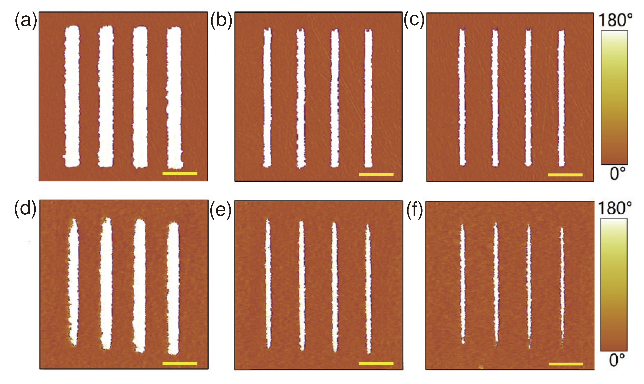
To begin with, we will explore the thermal stability of nano-domains in lithium niobate thin films without any pre-heat treatment in this part. As QPM devices and ferroelectric domain memory are two important potential applications for domain structures, both stripe domains and dot domains were fabricated and studied. Here, the stripe domains were fabricated using a raster lithography method with an AFM-tip voltage of 35 V. The rate of lithography was fixed at Hz. Periodical stripe domains with a fixed period of 1 m and an averaged stripe length of ∼4 m but with different stripe widths of nm, 205 nm, and 156 nm, were fabricated. The PFM images of these as-written stripe domains were measured, and the results are shown in Figure 2a–c, respectively.
We confirmed experimentally that these as-written stripe domians were stable at room temperature, and no degradation was observed even for several days. Then, the stripe domains were thermally annealed at a high temperature for h and then cooled down naturally to room temperature in air again. For comparison, the PFM images of the stripe domains after the thermal annealing treatment are shown in Figure 2d–f, respectively. The stripe domains were significantly degraded in both width and length dimensions after the thermal annealing treatment.
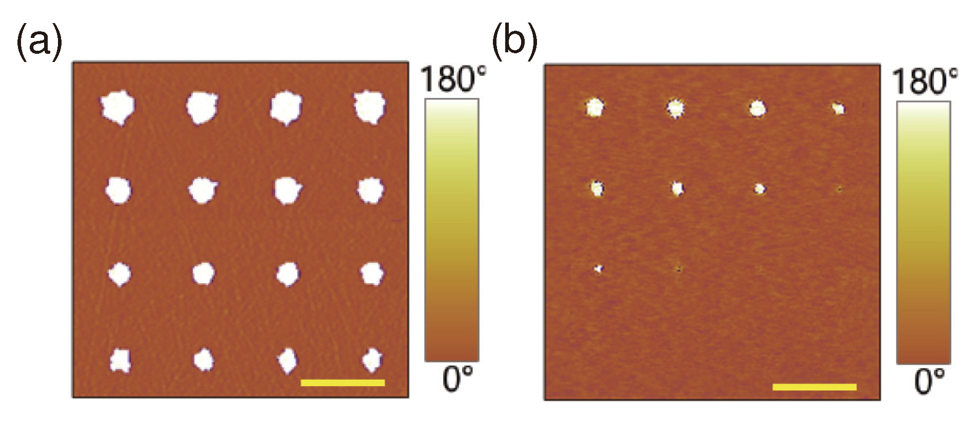
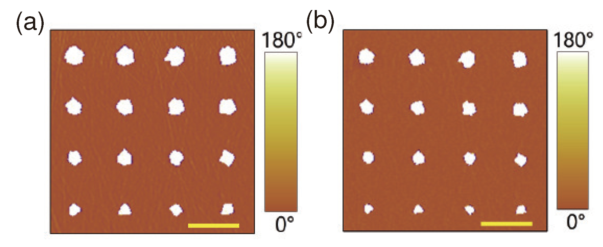
In addition, dot domains with different diameters were also fabricated by applying different AFM-tip voltages for a fixed time s. Each dot domain was separated from one another by 1 m in both the horizontal and vertical directions. Figure 3a shows the PFM images of the fabricated dot domains, in which four dot domains in each row were fabricated with the same tip voltage. These voltages were, from the bottom up, 40 V, 45 V, 50 V, and 55 V. The averaged diameter of the as-written dot domains in each row was measured to be 215 nm, 255 nm, 294 nm, and 333 nm, respectively. Here, the diameter D of a dot domain was estimated by equaling the area of the dot domain to a circle with a diameter D.
These as-written dot domains were also stable at room temperature. After that, the dot domains were annealed thermally at a high temperature C for one hour, and then the dot domains were cooled down to room temperature in air. Again, the PFM images of the dot domains after thermal annealing treatment were measured, and the results are shown in Figure 3b. It is evident that the dot domains are significantly degraded and even disappear for those small dot domains. This observed thermal instability is likely detrimental for practical applications such as QPM devices and ferroelectric domain memory devices.
3.2. Improvement on the Thermal Stability of Nano-Domains in Pre-Heated Lithium Niobate Thin Films
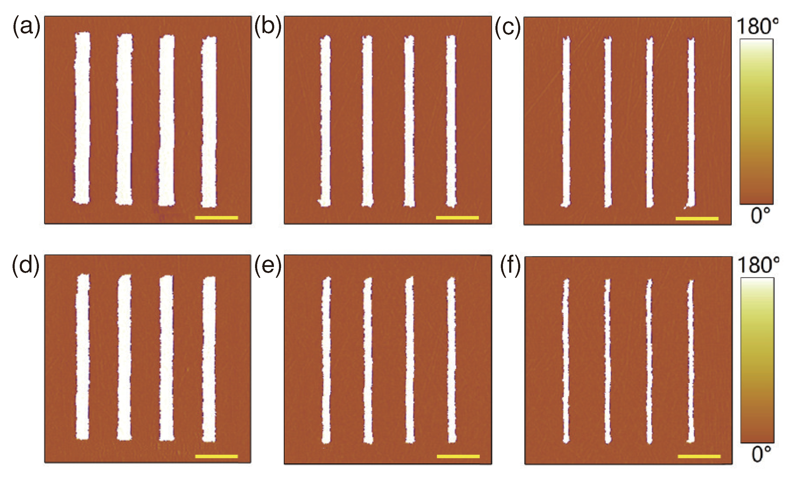
Here, we introduce a simple but effective way to improve the thermal stability of nano-domains in lithium niobate thin films. First, a virgin single-domain sample without any domain structures was put into the electric drying oven to undergo a pre-heat treatment at for 2 h. Then, nano-domains were written with the same tip voltage as those in Figure 2 for stripe domains and in Figure 3 for dot domains. In the experiments, the period of the stripe domains was set to be 1 m, and the width of the stripe domains was set to be 333 nm, 215 nm, and 137 nm, respectively. The PFM images of these as-written stripe domains were measured and are shown in Figure 4a–c, respectively.
After that, the sample with the stripe domains was thermally annealed at C for 1 h and then cooled down naturally to room temperature in air. The PFM images of the stripe domains were measured again for comparison, after the thermal annealing treatmen, and the results are shown in Figure 4d–f, respectively. As shown in Figure 4, although the stripe domains with a pre-heat treatment also degrade after the post-poling thermal annealing treatment, the degradation is significantly suppressed as compared to the case without the pre-heat treatment.
The thermal stability of the dot domains in the pre-heat treated samples was also studied. In the experiments, the dot domains were written in the pre-heat treated sample under the same tip voltage and writing time as those in Figure 3. Similarly, the separation distance between the nearest neighboring dot domains was set to be 1 m in both the horizontal and vertical dimensions, and dot domains with different averaged diameters of 215 nm, 255 nm, 294 nm, and 333 nm were prepared. Again, the diameters of the dot domains were averaged over four dot domains fabricated under the same tip voltage and writing time . Then, the sample with the dot domains underwent the same thermal annealing process as that in Figure 3.
The PFM images of the dot domains before and after the post-poling thermal annealing treatment were measured for comparison, and the results are shown in Figure 5. Compared to the case without pre-heat treatment in Figure 3, the thermal stability of the dot domains in the pre-heat treated samples is significantly improved.
4. Discussions
To show quantitatively the improvement on thermal stability of nano-domains in the pre-heat treated samples, we introduced a thermal stability parameter P, defined as , where and are the areas of the nano-domains before and after the post-poling thermal annealing treatment. The domain is more stable for a larger P. Table 1 lists the values of the thermal stability parameter P for both stripe domains and dot domains, as shown in Figure 2, Figure 3, Figure 4 and Figure 5.
In general, as compared to the case without pre-heat treatment, the thermal stability parameter P is much larger for nano-domains in the pre-heat treated samples, indicating that the thermal stability of nano-domains in samples with pre-heat treatment is significantly improved. Note that the length of stripe domains also shrinks, and the length shrinkages were measured to be 0.294 m, 0.235 m, and 0.588 m, in the case without pre-heat treatment, while in the case with pre-heat treatment, the length shrinkages were reduced to be 0.125 m, 0.121 m, and 0.093 m, for stripe domains with widths of 333 nm, 215 nm, and 137 nm, respectively.
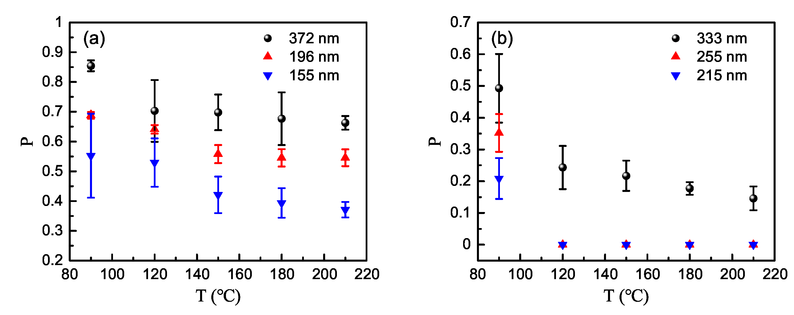
The dependence of the thermal stability parameter, P, on the post-poling annealing temperature, T, was studied for both stripe and dot domains without pre-heat treatment, and the results are shown in Figure 6. Here, stripe domains with different widths of 372 nm, 196 nm, and 155 nm and dot domains with different diameters of 333 nm, 255 nm, and 215 nm, were prepared. The length of all stripe domains was set to be ∼4 m. In all cases, the post-poling thermal annealing time, t, was set to be one hour. For both stripe domains and dot domains, the thermal stability parameter, P, decreases with the increase of the post-poling annealing temperature, T, and the domain degradation at 120 C is typical of the representative results within the studied temperature range, which is practically reachable in nano-size photonic structures, such as PPLN microcavities and PPLN ridge waveguides.
It has been reported that the domain structures in bulk lithium niobate crystals are stable at temperatures on the order of 100 C but decay also at a much higher temperature above 600 C [26,27], indicating that the domain structure in bulk crystal sheets is much more thermally stable when compared to that in lithium niobate thin films.
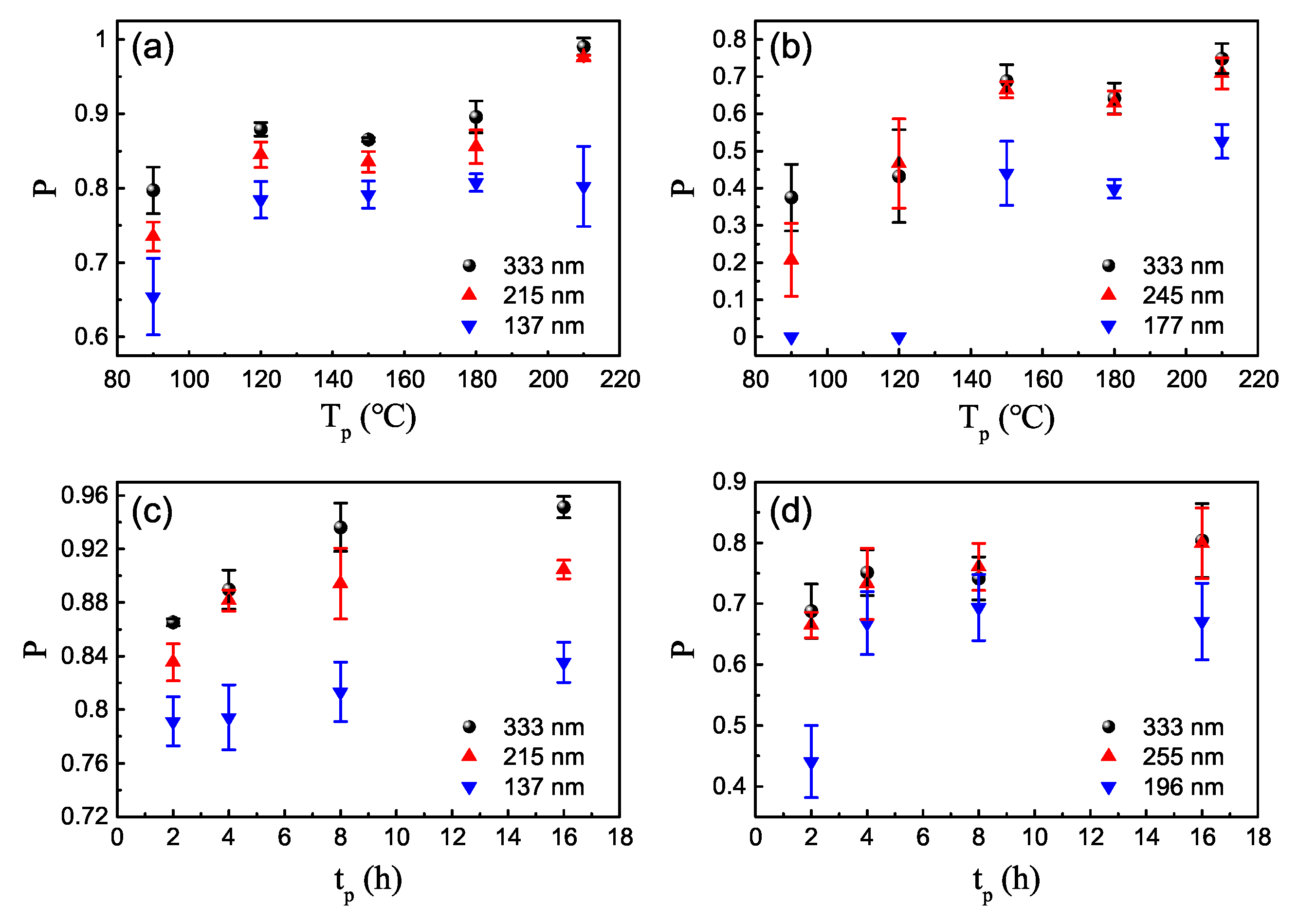
Furthermore, we studied the dependence of the thermal stability of nano-domains on the experimental pre-heat treatment conditions. In the experiments, pre-heat treatment on virgin single-domain samples was carried out at different high temperatures, , for different time periods, , and then stripe or dot domains with different sizes were fabricated by applying appropriate tip voltages. After that, the nano-domains were thermally annealed at C for 1 h. The PFM images of all nano-domains were measured and the thermal stability parameter P was characterized for each nano-domain.
Figure 7a,b shows the dependence of the thermal stability parameter, P, on the pre-heat temperature, , with h for the stripe domains and dot domains, with various sizes. P increases with the increase of the pre-heat temperature, , in both the stripe domain and the dot domain cases, indicating that the nano-domains are more thermally stable with higher . Figure 7c,d depicts the dependence of the thermal stability parameter, P, on the pre-heat time, , for the stripe and dot domains of various sizes. Here, the pre-heat treatment temperature was set to be 150 C for both cases. The thermal stability parameter P is larger with longer pre-heat treatment time, . In addition, the nano-domains with larger sizes are more stable for both cases, as shown in Figure 7.
From the above results, we see that domain degradation or even domain back switching may occur in lithium niobate thin films during a thermal annealing process at temperatures on the order of a hundred degrees Celsius. Fortunately, such domain degradation or back switching can be greatly suppressed through a simple pre-heat treatment for the virgin single-domain lithium niobate thin films. It is well known that the domain kinetics in ferroelectric lithium niobate are related to the local field distribution within lithium niobate crystals. At room temperature, the depolarization field, , is fully compensated by the screening field, , due to surface charges or bulk charges in lithium niobate crystals. When the crystal temperature increases, the spontaneous polarization, , and therefore the depolarization field, , decreases. This breaks the balance between the depolarization field, , and the screening field, . Therefore, the thermally actived bulk charges, such as protons in lithium niobate may drift in bulk, or the surface charges may accumulated on the surface, to compensate for this field imbalance [28,29]. This will result in a space charge field, , in lithium niobate with its direction antiparallel to the spontaneous polarization, . It is this space charge field that results in the degradation or back switching of the nano-domains in lithium niobate thin films. Note that the component of the space charge field induced by the thermally activated charges are fixed after the crystal is cooled down to the room temperature. This space charge field component induced by the thermally activated charges in crystal is also formed during the pre-heat treatment, and its direction is antiparallel to the spontaneous polarization in the virgin single-domain crystals but parallel to the reversed spontaneous polarization of the stripe or dot domains, which, therefore, results in a great suppression on the degradation of nano-domains. Comprehensive domain kinetics in lithium niobite thin films are an interesting but complicated topic, and they surely deserve a full-length study beyond the scope of this paper; for more details, please refer to Ref. [30].
5. Conclusions
In conclusion, we demonstrated a simple yet effective way to improve the thermal stability of nano-domains fabricated in lithium niobate thin films. We confirmed that the nano-domains in lithium niobate thin films are thermally unstable even at a temperature on the order of ∼100 C, which can be easily reached locally in nano-size photonic structures, due to light absorption. Therefore, such thermal instability of nano-domains could be very detrimental to practical applications, such as PPLN microcavities, PPLN ridge waveguides, and ferroelectric domain memories. We demonstrated that the thermal stability of nano-domains can be greatly improved when the lithium niobate thin film undergoes a pre-heat treatment before the fabrication of nano-domains. This thermal stability improvement is attributed to the generation of a space charge field during the pre-heat treatment, which is parallel to the spontaneous polarization of nano-domains. Our results should be useful for nano-domain-based photonic devices such as PPLN microcavities, PPLN ridge waveguides, and ferroelectric domain memories.
Author Contributions
G.Z. conceived the idea of the work. Y.J. designed and performed the experiments. Z.S. and S.L. participated in the experiments. Y.J. and G.Z. wrote the paper. All authors participated in the data analysis and paper preparation. All authors have read and agreed to the published version of the manuscript.
Acknowledgments
This work was supported by the National Natural Science Foundation of China (NSFC) (11774182, 61475077); the 111 project (B07013); and the Fundamental Research Funds for the Central Universities.
Conflicts of Interest
The authors declare no conflict of interest.
References
- Turner, E. High-Frequency Electro-Optic Coefficients of Lithium Niobate. Appl. Phys. Lett. 1966, 8, 303–304. [Google Scholar] [CrossRef]
- Kanno, A.; Sakamoto, T.; Chiba, A.; Kawanishi, T.; Higuma, K.; Sudou, M.; Ichikawa, J. 120-Gb/s NRZ-DQPSK signal generation by a thin-lithium-niobate-substrate modulator. IEICE Electron. Express 2010, 7, 817–822. [Google Scholar] [CrossRef] [Green Version]
- Courjal, N.; Benchabane, S.; Dahdah, J.; Ulliac, G.; Gruson, Y.; Laude, V. Acousto-optically tunable lithium niobate photonic crystal. Appl. Phys. Lett. 2010, 96, 131103. [Google Scholar] [CrossRef] [Green Version]
- Hao, Z.; Wang, J.; Ma, S.; Mao, W.; Bo, F.; Gao, F.; Zhang, G.; Xu, J. Sum-frequency generation in on-chip lithium niobate microdisk resonators. Photonics Res. 2017, 5, 623–628. [Google Scholar] [CrossRef]
- Wang, C.; Xiong, X.; Andrade, N.; Venkataraman, V.; Ren, X.F.; Guo, G.C.; Lončar, M. Second harmonic generation in nano-structured thin-film lithium niobate waveguides. Opt. Express 2017, 25, 6963–6973. [Google Scholar] [CrossRef] [PubMed] [Green Version]
- Hu, H.; Yang, J.; Gui, L.; Sohler, W. Lithium niobate-on-insulator (LNOI): status and perspectives. Silicon Photonics and Photonic Integrated Circuits III. Int. Soc. Opt. Photonics 2012, 8431, 84311D. [Google Scholar]
- Poberaj, G.; Hu, H.; Sohler, W.; Guenter, P. Lithium niobate on insulator (LNOI) for micro-photonic devices. Laser Photonics Rev. 2012, 6, 488–503. [Google Scholar] [CrossRef]
- Levy, M.; Osgood, R., Jr.; Liu, R.; Cross, L.; Cargill, G., III; Kumar, A.; Bakhru, H. Fabrication of single-crystal lithium niobate films by crystal ion slicing. Appl. Phys. Lett. 1998, 73, 2293–2295. [Google Scholar] [CrossRef]
- Li, Y.; Wang, C.; Loncar, M. Design of nano-groove photonic crystal cavities in lithium niobate. Opt. Lett. 2015, 40, 2902–2905. [Google Scholar] [CrossRef]
- Wang, J.; Bo, F.; Wan, S.; Li, W.; Gao, F.; Li, J.; Zhang, G.; Xu, J. High-Q lithium niobate microdisk resonators on a chip for efficient electro-optic modulation. Opt. Express 2015, 23, 23072–23078. [Google Scholar] [CrossRef] [Green Version]
- Rabiei, P.; Steier, W.H. Lithium niobate ridge waveguides and modulators fabricated using smart guide. Appl. Phys. Lett. 2005, 86, 161115. [Google Scholar] [CrossRef]
- Weigel, P.O.; Savanier, M.; DeRose, C.T.; Pomerene, A.T.; Starbuck, A.L.; Lentine, A.L.; Stenger, V.; Mookherjea, S. Lightwave circuits in lithium niobate through hybrid waveguides with silicon photonics. Sci. Rep. 2016, 6, 22301. [Google Scholar] [CrossRef] [PubMed] [Green Version]
- Gainutdinov, R.; Volk, T.; Zhang, H. Domain formation and polarization reversal under atomic force microscopy-tip voltages in ion-sliced LiNbO3 films on SiO2/LiNbO3 substrates. Appl. Phys. Lett. 2015, 107, 162903. [Google Scholar] [CrossRef]
- Hao, Z.; Zhang, L.; Gao, A.; Mao, W.; Lyu, X.; Gao, X.; Bo, F.; Gao, F.; Zhang, G.; Xu, J. Periodically poled lithium niobate whispering gallery mode microcavities on a chip. Sci. China-Phys. Mech. Astron. 2018, 61, 114211. [Google Scholar] [CrossRef]
- Wang, C.; Langrock, C.; Marandi, A.; Jankowski, M.; Zhang, M.; Desiatov, B.; Fejer, M.M.; Loncar, M. Ultrahigh-efficiency wavelength conversion in nanophotonic periodically poled lithium niobate waveguides. Optica 2018, 5, 1438–1441. [Google Scholar] [CrossRef] [Green Version]
- Garcia, V.; Fusil, S.; Bouzehouane, K.; Enouz-Vedrenne, S.; Mathur, N.D.; Barthelemy, A.; Bibes, M. Giant tunnel electroresistance for non-destructive readout of ferroelectric states. Nature 2009, 460, 81–84. [Google Scholar] [CrossRef] [PubMed]
- Guo, R.; You, L.; Zhou, Y.; Lim, Z.S.; Zou, X.; Chen, L.; Ramesh, R.; Wang, J. Non-volatile memory based on the ferroelectric photovoltaic effect. Nat. Commun. 2013, 4, 1990. [Google Scholar] [CrossRef] [Green Version]
- Sharma, P.; Zhang, Q.; Sando, D.; Lei, C.H.; Liu, Y.; Li, J.; Nagarajan, V.; Seidel, J. Nonvolatile ferroelectric domain wall memory. Sci. Adv. 2017, 3, e1700512. [Google Scholar] [CrossRef] [Green Version]
- Jiang, J.; Bai, Z.L.; Chen, Z.H.; He, L.; Zhang, D.W.; Zhang, Q.H.; Shi, J.A.; Park, M.H.; Scott, J.F.; Hwang, C.S.; et al. Temporary formation of highly conducting domain walls for non-destructive read-out of ferroelectric domain-wall resistance switching memories. Nat. Mater. 2018, 17, 49–56. [Google Scholar] [CrossRef] [Green Version]
- Lindgren, G.; Pena, A.; Zukauskas, A.; Liljestrand, C.; Menaert, B.; Boulanger, B.; Canalias, C. Thermal stability of ferroelectric domain gratings in Rb-doped KTP. Appl. Phys. Lett. 2015, 107, 082906. [Google Scholar] [CrossRef]
- Liu, X.; Kitamura, K.; Terabe, K. Thermal stability of LiTaO3 domains engineered by scanning force microscopy. Appl. Phys. Lett. 2006, 89, 142906. [Google Scholar] [CrossRef]
- Woo, J.; Hong, S.; Min, D.K.; Shin, H.; No, K. Effect of domain structure on thermal stability of nanoscale ferroelectric domains. Appl. Phys. Lett. 2002, 80, 4000–4002. [Google Scholar] [CrossRef]
- Liu, X.Y.; Kitamura, K.; Liu, Y.M.; Ohuchi, F.S.; Li, J.Y. Thermal-induced domain wall motion of tip-inverted micro/nanodomains in near-stoichiometric LiNbO3 crystals. J. Appl. Phys. 2011, 110, 052009. [Google Scholar] [CrossRef]
- Shur, V.Y.; Mingaliev, E.A.; Lebedev, V.A.; Kuznetsov, D.K.; Fursov, D.V. Polarization reversal induced by heating-cooling cycles in MgO doped lithium niobate crystals. J. Appl. Phys. 2013, 113, 187211. [Google Scholar] [CrossRef] [Green Version]
- Shao, G.H.; Bai, Y.H.; Cui, G.X.; Li, C.; Qiu, X.B.; Geng, D.Q.; Wu, D.; Lu, Y.Q. Ferroelectric domain inversion and its stability in lithium niobate thin film on insulator with different thicknesses. AIP Adv. 2016, 6, 075011. [Google Scholar] [CrossRef] [Green Version]
- Saveliev, E.D.; Saveliev, A.P.; Akhmatkhanov, A.R.; Baturin, I.S.; Ya Shur, V. Annealing stability of the domain structure in periodically poled MgO doped lithium niobate single crystals. Ferroelectrics 2019, 542, 45–51. [Google Scholar] [CrossRef]
- Yamada, M.; Saitoh, M. Fabrication of a periodically poled laminar domain structure with a pitch of a few micrometers by applying an external electric field. J. Appl. Phys. 1998, 84, 2199–2206. [Google Scholar] [CrossRef]
- Imbrock, J.; Hanafi, H.; Ayoub, M.; Denz, C. Local domain inversion in MgO-doped lithium niobate by pyroelectric field-assisted femtosecond laser lithography. Appl. Phys. Lett. 2018, 113, 252901. [Google Scholar] [CrossRef] [Green Version]
- Shur, V.Y.; Rumyantsev, E.; Batchko, R.; Miller, G.; Fejer, M.; Byer, R. Domain kinetics in the formation of a periodic domain structure in lithium niobate. Phys. Solid State 1999, 41, 1681–1687. [Google Scholar] [CrossRef]
- Shur, V.Y. Kinetics of ferroelectric domains: Application of general approach to LiNbO3 and LiTaO3. J. Mater. Sci. 2006, 41, 199–210. [Google Scholar] [CrossRef]
Figure 1.
Schematic diagram of nano-domain writing in lithium niobate film on insulators (LNOI) under an atomic force microscope (AFM)-tip voltage.
Figure 1.
Schematic diagram of nano-domain writing in lithium niobate film on insulators (LNOI) under an atomic force microscope (AFM)-tip voltage.

Figure 2.
(a–c) Piezoresponse force microscope (PFM) images of as-written stripe domains with different stripe widths before the thermal annealing treatment. (d–f) The corresponding PFM images of stripe domains after the thermal annealing treatment at C for 1 h. The length of the stripe domains was set to be ∼ 4 m. The scale bar in all figures is 1 m.

Figure 3.
(a) PFM images of as-written dot domains with different diameters before the thermal annealing treatment. (b) The corresponding PFM images of dot domains after the thermal annealing treatment, at a temperature C for 1 h. Here, the dot domains in each row were fabricated at the same AFM-tip voltage. These voltages were, from the bottom up, 40 V, 45 V, 50 V, and 55 V. The scale bar was 1 m in both cases.

Figure 4.
The thermal stability of stripe domains in a sample that underwent a pre-heat treatment at C for 2 h. (a–c) PFM images of as-written stripe domains before the thermal annealing treatment. (d–f) PFM images of stripe domains after the thermal annealing treatment at 120 C for 1 h. The length of the stripe domains was set to be ∼ 4 m. Here, the tip voltage used to fabricate the stripe domains was the same as that in Figure 2. The scale bar is 1 m in all figures.

Figure 5.
Thermal stability of the dot domains in a sample that underwent a pre-heat treatment at C for 2 h. (a) PFM images of as-written dot domains with different diameters before the thermal annealing treatment. (b) PFM images of dot domains after the thermal annealing treatment at 120C for 1 h. Here, the dot domains in each row were fabricated at the same AFM-tip voltage as those in Fig. Figure 3. The scale bar is 1 m in all figures.

Figure 6.
The dependence of the thermal stability parameter, P, on the post-poling annealing temperature T for both stripe domains (a) and dot domains (b) of various sizes without pre-heat treatment. Here, the post-poling thermal annealing time t was set to be 1 h in all cases, and the length of the stripe domains was set to be ∼4 m.

Figure 7.
Dependence of the thermal stability parameter, P, on the pre-heat temperature, , (a,b) and the pre-heat time, , (c,d), for nano-domains with various sizes. Here, (a,c) are the results for the stripe domains, while (b,d) are the results for the dot domains. The pre-heat time, , was 2 hours for (a,b), while the pre-heat temperature, , was set to be 150 C for (c,d). All nano-domains were thermally annealed at C for 1 h.


Table 1.
The thermal stability parameter, P, of nano-domains in samples with or without pre-heat treatment. The condition of pre-heat treatment was C for 2 hours. The length of the stripe domains was set to be ∼4 m.
Table 1.
The thermal stability parameter, P, of nano-domains in samples with or without pre-heat treatment. The condition of pre-heat treatment was C for 2 hours. The length of the stripe domains was set to be ∼4 m.
| Domain Size | Width of Stripe Domains | Diameter of Dot Domains | ||||
|---|---|---|---|---|---|---|
| 333 nm | 215 nm | 137 nm | 333 nm | 255 nm | 215 nm | |
| without pre-heat treatment | 0.69 | 0.64 | 0.52 | 0.24 | 0 | 0 |
| with pre-heat treatment | 0.86 | 0.83 | 0.79 | 0.72 | 0.66 | 0.56 |
© 2020 by the authors. Licensee MDPI, Basel, Switzerland. This article is an open access article distributed under the terms and conditions of the Creative Commons Attribution (CC BY) license (http://creativecommons.org/licenses/by/4.0/).
Share and Cite
MDPI and ACS Style
Jiao, Y.; Shao, Z.; Li, S.; Wang, X.; Bo, F.; Xu, J.; Zhang, G. Improvement on Thermal Stability of Nano-Domains in Lithium Niobate Thin Films. Crystals 2020, 10, 74. https://0-doi-org.brum.beds.ac.uk/10.3390/cryst10020074
AMA Style
Jiao Y, Shao Z, Li S, Wang X, Bo F, Xu J, Zhang G. Improvement on Thermal Stability of Nano-Domains in Lithium Niobate Thin Films. Crystals. 2020; 10(2):74. https://0-doi-org.brum.beds.ac.uk/10.3390/cryst10020074
Chicago/Turabian StyleJiao, Yuejian, Zhen Shao, Sanbing Li, Xiaojie Wang, Fang Bo, Jingjun Xu, and Guoquan Zhang. 2020. "Improvement on Thermal Stability of Nano-Domains in Lithium Niobate Thin Films" Crystals 10, no. 2: 74. https://0-doi-org.brum.beds.ac.uk/10.3390/cryst10020074
Note that from the first issue of 2016, this journal uses article numbers instead of page numbers. See further details here.