Article

Efficient Broadband Truncated-Pyramid-Based Metamaterial Absorber in the Visible and Near-Infrared Regions

1
Future Semiconductor Convergence Technology Research Center, Division of Electronics Engineering, Jeonbuk National University, Jeonju 54896, Korea
2
Division of Computational Physics, Institute for Computational Science, Ton Duc Thang University, Ho Chi Minh City 700000, Vietnam
3
Faculty of Electrical & Electronics Engineering, Ton Duc Thang University, Ho Chi Minh City 700000, Vietnam
*
Authors to whom correspondence should be addressed.
Submission received: 13 August 2020 / Revised: 31 August 2020 / Accepted: 1 September 2020 / Published: 3 September 2020
(This article belongs to the Special Issue Plasmonic Nanostructures)

Abstract

:
We present a design of an ultra-broadband metamaterial absorber in the visible and near- infrared regions. The unit cell structure consists of a single layer of metallic truncated-pyramid resonator-dielectric-metal configuration, which results in a high absorption over a broad wavelength range. The absorber exhibits 98% absorption at normal incidence spanning a wideband range of 417–1091 nm, with >99% absorption within 822–1054 nm. The broadband absorption stability maintains 95% at large incident angles up to 40° for the transverse electric (TE)-mode and 20° for the transverse magnetic (TM)-mode. Furthermore, the polarization-insensitive broadband absorption is presented in this paper by analyzing absorption performance with various polarization angles. The proposed absorber can be applied for applications such as solar cells, infrared detection, and communication systems thanks to the convenient and compatible bandwidth for electronic THz sources.

1. Introduction

Nowadays, the metamaterial absorber (MA) has drawn substantial attention for both fundamental studies and practical applications due to its high applicability in the microwave MA with near-unity absorption intensity [1], the surface-enhanced sensing, and ultra-sensitive sensing [2,3]. Generally, the subwavelength MA structure is designed based on the metal–dielectric–metal (MDM) interface. The interface can be tailored flexibly owing to the generation of artificial meta-atoms at the interface. The MDM configuration enables the enhanced absorption intensity of the MA [4,5]. The absorption property plays a particularly important role in solar cells and high-performance photodetectors [6,7,8,9,10,11,12,13,14,15,16,17]. Up to now, many technologies have been proposed to enhance the light absorption of the plasmonic metamaterial structures in both the intensity and broadband. For instance, various metallic reflectors and gratings where patterned surfaces with different shapes and sizes are designed and deposited on the dielectric layer have been reported.
The absorption peaks can be tuned by optimizing the shaped metallic grating structure located at the top of the MA. Recently, many efforts have been studied to widen the absorption bandwidth by using multi-shaped metallic configurations stacking of dielectric-meta layers [18,19], hole-arrays working as resonators [20], the shaped rectangular grating [21], shaped L grating [22,23], cylinder array [24], epsilon-near-zero (ENZ) materials [25,26], nanoporous materials that exhibit high efficiency in terms of broadband absorption, as well as their high applicability in sensors and easily fabricable devices [27,28,29,30]. However, these MA structures still have many disadvantages such as narrow absorption bandwidth, and polarization sensitivity due to the asymmetry structures having a low order of rotational symmetry, whereas many practical applications require the polarization-insensitive feature. For instance, a subwavelength nanostructure based on the MDM configuration with top crossed trapezoidal array silver geometry was proposed in the literature [31]. It can obtain a 71% average absorption in the visible region with a bandwidth of 300 nm (from 400 to 700 nm), while an absorber with a quasi-periodic gold nano-cone-shaped grating can reach an absorption of 87.4% in the range of 300–700 nm [32]. Moreover, the configuration of a thin-material nanostructure with a periodic array of titanium and silicon dioxide cubes, and aluminum as a bottom film can realize a 90% absorption bandwidth over 700 nm (from 354 to 1066 nm) [19]. However, Lei et al. did not explain the mechanism of the MA through the numerical analysis of the effective parameters, e.g., the effective impedance z [4]. Furthermore, the wavelength band over 712 nm is still not enough to meet the increasing requirements of harvesting solar energy applications, which require an inherently ultra-wideband with near-perfect absorption.
In this paper, we introduce an innovative wideband MA from visible light to near-infrared light regions based on a thin metamaterial nanostructure with a truncated-pyramid metallic resonator. In the previous study, the efficiency of the rectangular metallic-shaped gratings and the taper-shaped metallic gratings was demonstrated in a high-index contrast medium [12]. As a result, a plasmonic structure with metallic rectangular gratings had high reflection due to the significant mismatch between the entrance and exit faces of the impedance of the structure. We proposed the tapered metallic grating to enable impedance matching and reflection reduction over a broad bandwidth. The device structure is an MDM configuration composed of a periodic array of titanium (Ti) truncated-pyramid metallic gratings, a silicon dioxide (SiO2) dielectric spacer layer, and an optically thick titanium nitride (TiN) as a bottom film. Our simulation results show an extremely high absorption (>98%) with a broad bandwidth from visible light to near-infrared light regions. Furthermore, the physical mechanism of the MA structure is explained through the effective impedance parameter of a homogeneous structure by using the retrieval method [33].

2. Structure Design and Methods

The geometric structure of the proposed truncated-pyramid MA is shown in Figure 1. The MA structure was designed on a 250 nm supporting metallic substrate made from titanium nitride (TiN). We utilized the commercial software package COMSOL Multiphysics® Version 5.5 software (COMSOL, Inc. Stockholm, Sweden) [34] to simulate the periodic structure of the MA device with appropriate boundary conditions. We set-up a periodic structure with the boundary conditions using a Floquet-port at the apex and bottom of the structure, and the corresponding perfectly matched layers (PML) were applied to excommunicate the surface scattering. The electromagnetic wave is polarized as a plane wave along the z-axis, and they will be reflected or absorbed depending on the impedance matching of the MA structure and the surrounding environment. Therefore, the effective impedance z is exploited through a periodic structure with reflection (S11) and transmission (S21) parameters. The relationship between the z, S11, and S21 parameters will be shown in the next section. The dispersive properties of TiN, SiO2, and Ti layers were extracted from the material library of the commercial software package COMSOL Multiphysics software while the surrounding medium was air. The refractive indices of Ti and TiN have been calculated by Rakić et al. [35] and Pflüger et al. [36], respectively, and the refractive index of the SiO2 is 1.45.
For the device, the absorption band can be extended significantly with the higher absorptivity in the visible and near-infrared regions through the optimized process. Based on the optimized results, we determined that the optimized geometrical parameters of metallic truncated-pyramid gratings were as follows: The height of the grating (h), upper face of the grating (Wi), and lower face the grating (Wo) are 140, 70, and 140 nm, respectively. The periodicity P is 200 nm. The thickness of the SiO2 layer (td) is 25 nm to separate the two metallic layers. In the study, the absorption of the MA structure can be calculated through the relationship between absorption (A) and reflection (R) by the simple expression of A = 1 − R due to the thickness of the back reflector metallic layer in this structure being larger than the penetration depth of the TiN material (~63.2 nm at 413.3 nm wavelength), i.e., the transmission is zero. We will present a concise and precise description of the optimal simulated results, the physical mechanism of the MA structure, and the conclusions in the next sections.
The proposed truncated-pyramid MA can be fabricated by focus-ion-beam (FIB) technology [37]. A phase mask of various ion doses can be designed for generating the array of Ti-truncated pyramids using a pattern generator. The pattern can be transferred into the Ti film by direct milling.

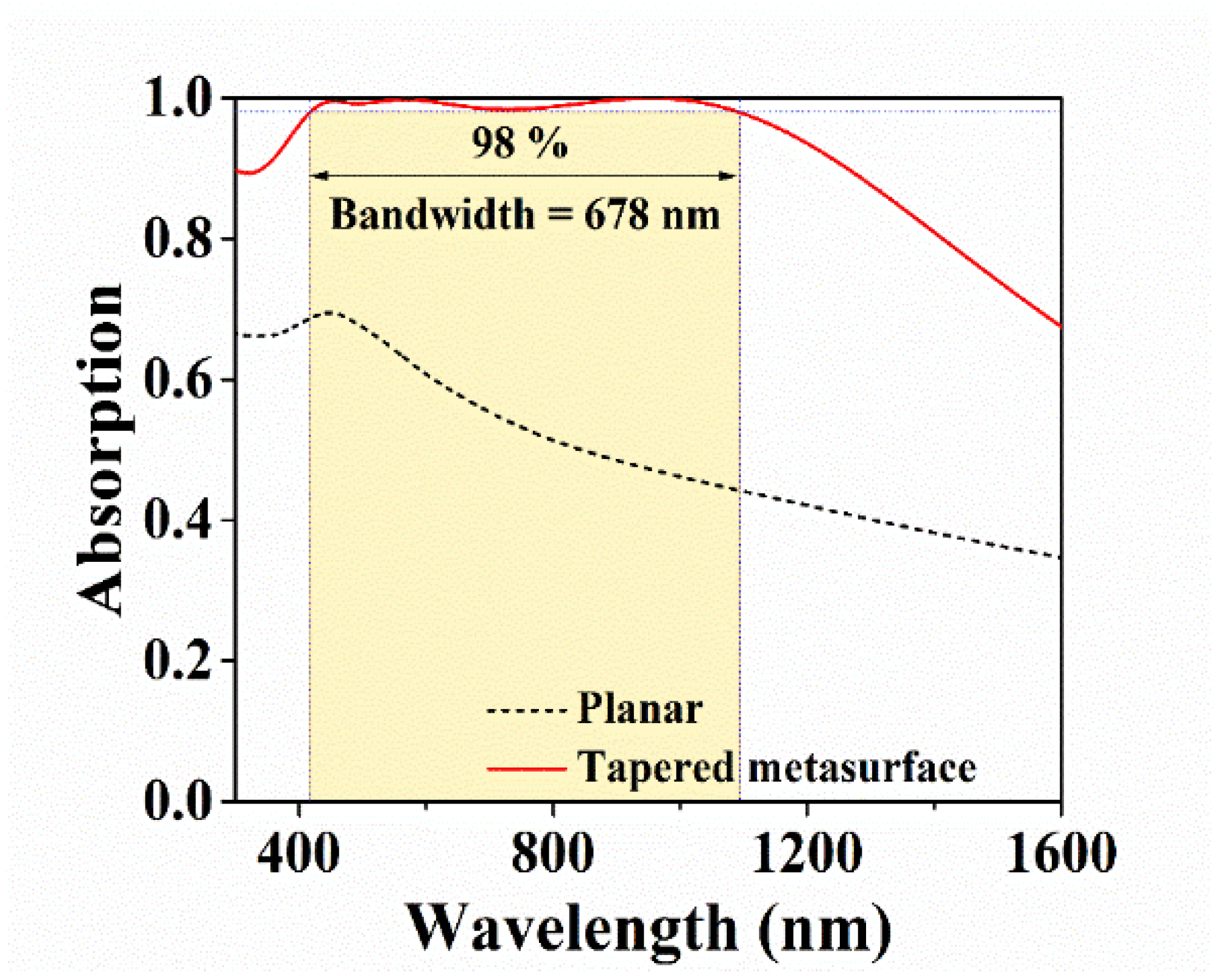
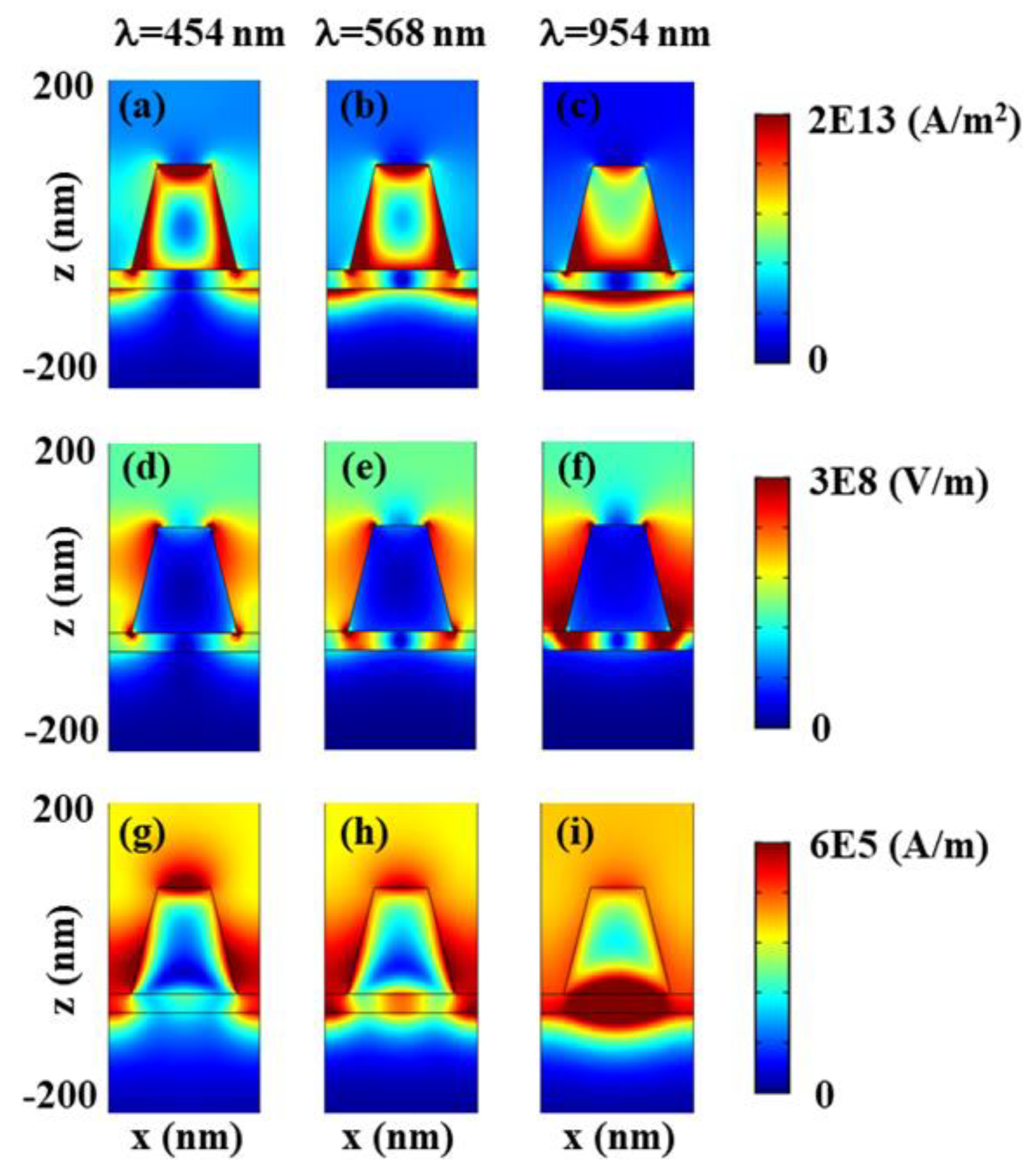
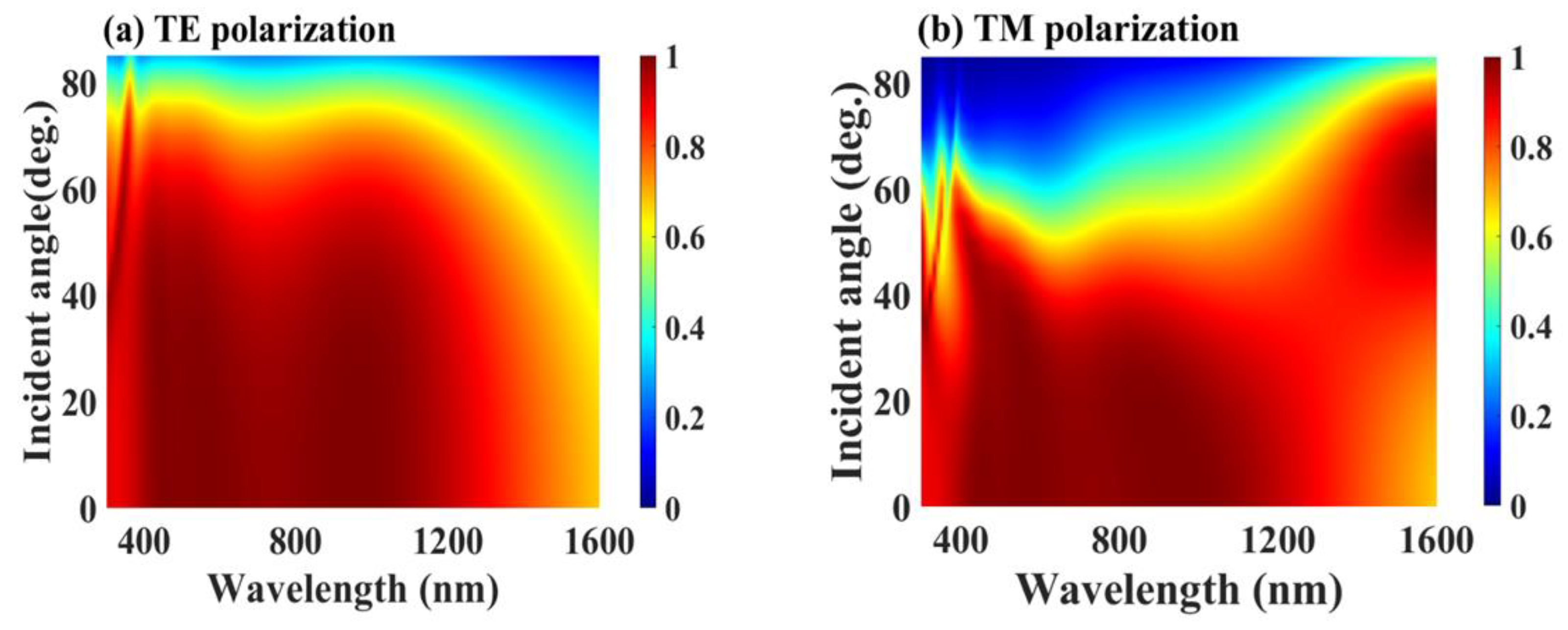
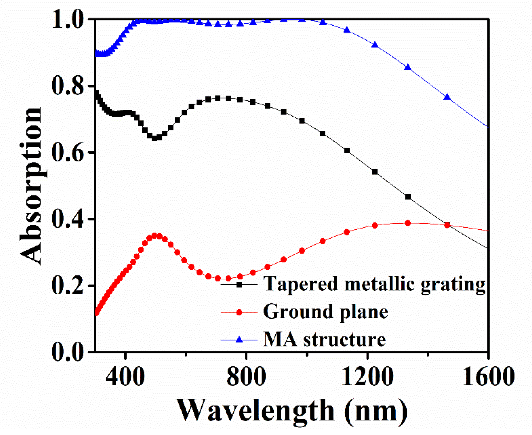
3. Results and Discussion

The proposed truncated-pyramid MA structure (as seen in Figure 1) is expected to be able to generate localized surface plasmon resonance (LSPR) modes [38] at the top truncated-pyramid grating-insulator-metallic film layer interfaces. In addition, these LSPR modes can couple to the propagating surface plasmon resonance (PSPR) modes [39] occurring at the interface of the SiO2 layer and TiN back metallic reflector film that results in the enhancement of absorption spectra in the MA device. As demonstrated in our previous work [6], the tapered metallic grating activates the impedance matching in order to enhance light absorption over a broad bandwidth. It is expected to enhance absorption intensity in the same way as the other kind of metallic gratings [40].
The absorption spectra of the proposed MA device at normal incidence are shown in Figure 2. It exhibits a high absorption of 95% over a broad bandwidth of 781 nm (from 390 to 1171 nm) and a near-perfect absorption of approximately 98% over a wavelength range from 416 to 1094 nm, indicating a broad bandwidth of 678 nm from the visible to near-infrared regimes. In addition, a broad bandwidth of 232 nm (from 822 to 1054 nm) with >99% absorption is also exhibited around a resonant wavelength of 955 nm. The absorption mechanism of the MA device can be clarified by the theory of the plasmonic effect of metallic nanoparticles [41]. The effect causes extremely strong electromagnetic resonances at the various resonant wavelengths. The plasmonic mechanism is generally based on the LSPR modes and the PSPR modes, and the coupling of both LSPR modes and PSPR modes dominates the absorption. Moreover, the coupling of the light and the air-slot is generated from the tapered grating corners between the adjacent unit cells that results in the generated surface plasmon polaritons (SPPs) [42]-induced light absorption. The presence of SPPs can be verified in the absorption spectra of the proposed MA structure with its planar counterpart, as shown in Figure 2. The absorption of the proposed MA structure is significantly stronger than that of the planar structure in the whole wavelength region from the visible to near-infrared due to the SPPs enhancement.
To clarify the physical mechanism of the proposed MA structure, we investigated the current density, electronic field distribution, and magnetic field distribution under TE-polarization at the three resonant wavelengths, corresponding to the three peaks of the absorption spectrum. Figure 3 shows the current density, and electric and magnetic field distributions at various resonant wavelengths of 454, 568, and 954 nm in the XZ-plane, respectively. The current density is mainly located in the truncated metallic grating and partially in the dielectric gap where the LSPR is excited by the interface of the MDM configuration, as seen in Figure 3a–c. The enhancement of broad bandwidth absorption can be clarified by the current density distribution causing the energy loss [19]. Furthermore, we investigated the electrical distribution to confirm the presence of SPPs confined in the dielectric layer and located around the corners of the truncated metallic grating. Figure 3d–f shows the presence of SPPs. At the resonant wavelength of 954 nm, a strong coupling between the air-slot and the truncated metallic grating is exhibited in Figure 3f. The physical explanation can be understood when the MA structure has the presence of a propagating electromagnetic wave inducing the electric fields and currents in the patterned truncated grating and the dielectric layer. The strong field located in the truncated grating is due to the high charge concentration at these metallic edges. On the other hand, the electric fields and currents are generated in the opposite direction from the conductive back metallic film TiN to that of fields in the truncated grating thanks to the near-field coupling, resulting in the antiparallel currents creating the magnetic field in the gap dielectric layer.
Figure 3g–i show the magnetic field distribution for light absorption. The excitation of the LSPR modes generated at the truncated grating/dielectric layer interface and PSPR modes excited at the dielectric layer/TiN back reflector interface are observed. We see that at 954 nm (as in Figure 3i), the magnetic field enhancement is strongly located in the dielectric gap between the truncated grating and metallic reflector, indicating evidence for this coupling. Therefore, it provides strong confinement of incident light in the truncated resonator, which results in the enhanced light absorption.
In the simulated model, we set-up a periodic structure with the boundary conditions using the Floquet-port at the two ends of the structure, and a perfectly matched layer (PML) was used to eliminate the surface scattering. By using numerical analysis, we extracted the effective impedance z from Equation (1) [33], where S11 and S21 are the reflections and the transmission parameters exploited from the two-port model of the structure.
z =   ± ( 1 + S 11 ) 2 S 21 2 ( 1 S 11 ) 2 S 21 2
Due to the MA being backed by a metallic film, Equation (1) will be shortened as follows,
z =   ± ( 1 + S 11 ) 2 ( 1 S 11 ) 2   =   | 1 + S 11 1     S 11 |
The broadband absorption of the device can be realized by the values of the effective impedance z including the real part (near 1) and imaginary part (near zero), as seen in Figure 4. This indicates that the absorption is greatest and the perfect wideband as the real part of z matches completely to free space (i.e., equal to 1 or unity), while the imaginary part is zero in the whole range of interest. Otherwise, when z between the MA device and free space is not matched, it results in increased reflection and reduced absorption. Furthermore, the dispersion properties of metallic components in the MA structure are also an important factor determining the efficient absorption. As shown in Figure 4, the values of z in the imaginary part indicate that the values are near zero in the corresponding wavelength range with absorption bandwidth at the resonant peaks, as shown in Figure 2. In addition, the real part of z is near-unity, which further reinforces the correctness of the mechanism.
Absorption for oblique incidences plays a very important role in the optical distribution of the MA structure. The performance decreases gradually from large oblique angles. To better understand the performance of the proposed MA device, we calculate the absorption as a function of incident angles from 0 to 85° by a step of 5° for both the TE-mode and TM-mode. Figure 5 shows the specific simulated results. The proposed truncated MA device exhibits stability absorption at small incident angles from 0 to 40° for the TE-mode, as depicted in Figure 5a, and from 0 to 30° for the TM-mode, as depicted in Figure 5b. For the TM-mode, one more resonant peak broadened beyond 1600 nm appears in the absorption spectra due to the enhancement of the coupling of resonant modes at longer wavelengths. Here, the absorption intensity is estimated higher than 98% in the range of wavelengths from 1500 to 1600 nm at an incident angle of 62°. For the TE-mode, the absorption bandwidth is unchanged essentially for incident angles less than 40°, while for the TM-mode, this range is decreased when the angles are over 20°. It can be seen that, at angles over 20°, the absorption bandwidth in the TE-mode is wider and more stable than the absorption bandwidth of the TM-mode because the optical cavities create temporal and spatial interference in the dielectric layer and the truncated grating resonators in which plasmonic resonant modes modify the angular response.
Figure 6 shows the absorption ability of the metallic truncated grating and ground plane serving as a back reflector. The absorption loss is significantly dominated by the top resonator while that of the bottom film dominates slightly in the wavelength range of interest. There are two characteristic peaks at 500 and 1340 nm in the absorption spectra of the bottom metallic film, indicating the role of PSPR and LSPR resonances, respectively. Moreover, the physical mechanism in the absorption of the truncated metallic resonator can be explained as follows. The top resonator allows the impinging incident waves to tunnel and the energy to squeeze through the truncated grating to the spacer when the light wave propagates through the device. The obtained absorption is perfect only if the coupling conditions are satisfied such as the permittivity and thickness of the top metallic grating exciting the cavity modes, as well as the intensity of the coupling between cavity modes and the incident waves. That is the reason why the top metallic grating significantly affects the strength of absorption and absorption bandwidth, which is the criteria to optimize the designed absorber.
Next, polarization insensitivity is evidenced in Figure 7, which depicts the simulated absorption spectra under normal incidence with various φ polarization angles. As seen in Figure 7, the polarization direction of the incident plane wave and electric (or magnetic as well) field is represented by the polarization angle φ. As the angle of polarization increases from 0 to 80° with the step of 20°, the absorption bandwidth is almost unchanged, which indicates that the absorption is completely independent to the polarization angle of the incident plane waves. As analyzed above, the broadband absorption is formed by the coupling of strong resonant frequencies. The coupling resonances of neighboring unit cells is weaker than those of the discrete elements. Thus, the polarization insensitivity can be performed thanks to the polarization-insensitive elements.
The polarization insensitivity is investigated for various oblique angles. Figure 8 depicts the results for both the TE-mode (as shown in Figure 8a–c) and TM-mode (as shown in Figure 8d–f) with incident angles of 20°, 30°, and 40°, respectively. The bandwidth-absorbing spectrum maintains a highly insensitive polarization until the angle of incidence is 30°, where the absorption spectra are slightly affected in the longer wavelength range while the polarization insensitivity is impossible at 40 ° in the whole wavelength range of interest.
Furthermore, the geometric effects of the truncated pyramid resonators are also investigated in Figure 9. The influence of the pyramid height (h) on the absorption performance is shown in Figure 9a. The ideal value of h is around 140 nm to achieve the highest absorption efficiency over the broad bandwidth as in the marked range. The absorption efficiency decreases significantly with the decrease or increase in h due to the relevant lossy cavity. As depicted in Figure 9b, the ratio of the pyramid (i.e., Wi/Wo) is a function of the lower face (Wo) of the pyramid. The effect of the upper face (Wi) and the lower face (Wo) of the pyramid is evaluated through the ratio Wi/Wo. Accordingly, the values of the ratio Wi/Wo to obtain an ideal average absorption as in the marked range are around 0.5 (i.e., Wi equal to 70 nm) and 140 nm, respectively. The change in Wi/Wo results in the change in the filling factor of the structure, which is related to the SPP resonances affecting the absorption performance.
In addition, the absorption efficiency of pillars replacing the pyramid in the system is shown in a broadband spectrum (Figure S1 from Supporting Information).

4. Conclusions

In summary, we have designed a truncated-pyramid MA structure in the visible and infrared regions based on a periodically patterned metal–dielectric–metal structure. The absorber exhibits a near-perfect absorption with a magnitude of absorption of 98% over a broadband of 674 nm from 417 to 1091 nm, while a 232 nm bandwidth (from 822 to 1054 nm) with >99% absorption is also obtained at around 954 nm. The strong coupling of plasmonic resonances between metals enables the enhanced absorption bandwidth. The absorption levels maintain 98% at angles up to 40° for the TE-mode and 20° for the TM-mode. In addition, the structure can achieve broadband polarization-independent absorption, which is expected to be applied in many practical applications i.e., detection, imaging, sensing, and defense applications. In addition, the MA structure is a potential candidate for light-harvesting applications in the visible and infrared ranges both in terms of extreme magnitude and broadband.

Supplementary Materials

The following is available online at https://0-www-mdpi-com.brum.beds.ac.uk/2073-4352/10/9/784/s1, Figure S1: The absorption performances of pillars (cylinder) and truncated pyramids with normally incident TE-polarized light. The height and radius of the pillar are 140 and 70 nm, respectively.

Author Contributions

Data curation, J.K., J.P., V.-C.N., D.D.V., T.K.N. and K.Q.L.; Investigation, P.T.D. and T.V.V.; Project administration, J.-H.L.; Writing—original draft, P.T.D.; Writing—review and editing, K.Q.L. and J.-H.L. All authors have read and agreed to the published version of the manuscript.

Funding

This research was funded by the National Research Foundation of Korea (grant numbers: 2019R1A2B5B01069580; 2019R1A6A1A09031717; 2019H1A2A1074764) and by the Ministry of Trade, Industry and Energy (grant number: 20011031).

Conflicts of Interest

The authors declare no conflict of interest.

References

  1. Landy, N.I.; Sajuyigbe, S.; Mock, J.J.; Smith, D.R.; Padilla, W.J. Perfect Metamaterial Absorber. Phys. Rev. Lett. 2008, 100, 207402. [Google Scholar] [CrossRef] [PubMed]
  2. Cong, L.; Tan, S.; Yahiaoui, R.; Yan, F.; Zhang, W.; Singh, R. Experimental demonstration of ultrasensitive sensing with terahertz metamaterial absorbers: A comparison with the metasurfaces. Appl. Phys. Lett. 2015, 106, 031107. [Google Scholar] [CrossRef]
  3. Singh, R.; Cao, W.; Al-Naib, I.; Cong, L.; Withayachumnankul, W.; Zhang, W. Ultrasensitive terahertz sensing with high-Q Fano resonances in metasurfaces. Appl. Phys. Lett. 2014, 105, 171101. [Google Scholar] [CrossRef] [Green Version]
  4. Ghobadi, A.; Hajian, H.; Rashed, A.R.; Butun, B.; Ozbay, E. Tuning the metal filling fraction in metal-insulator-metal ultra-broadband perfect absorbers to maximize the absorption bandwidth. Photon- Res. 2018, 6, 168–176. [Google Scholar] [CrossRef]
  5. Chen, Y.; Dai, J.; Yan, M.; Qiu, M. Metal-insulator-metal plasmonic absorbers: Influence of lattice. Opt. Express 2014, 22, 30807–30814. [Google Scholar] [CrossRef]
  6. Dang, P.T.; Nguyen, T.K.; Le, K.Q. Revisited design optimization of metallic gratings for plasmonic light-trapping enhancement in thin organic solar cells. Opt. Commun. 2017, 382, 241–245. [Google Scholar] [CrossRef]
  7. Nguyen, T.K.; Dang, P.T.; Le, K.Q. Numerical design of thin perovskite solar cell with fiber array-based anti-reflection front electrode for light-trapping enhancement. J. Opt. 2016, 18, 125901. [Google Scholar] [CrossRef]
  8. Costanzo, S.; Venneri, F. Polarization-Insensitive Fractal Metamaterial Surface for Energy Harvesting in IoT Applications. Electronics 2020, 9, 959. [Google Scholar] [CrossRef]
  9. Alam, A.; Islam, S.S.; Islam, H.; Almutairi, A.F.; Islam, M.T. Polarization-Independent Ultra-Wideband Metamaterial Absorber for Solar Harvesting at Infrared Regime. Materials 2020, 13, 2560. [Google Scholar] [CrossRef]
  10. Safaei, A.; Chandra, S.; Leuenberger, M.N.; Chanda, D. Wide Angle Dynamically Tunable Enhanced Infrared Absorption on Large-Area Nanopatterned Graphene. ACS Nano 2018, 13, 421–428. [Google Scholar] [CrossRef] [Green Version]
  11. Thongrattanasiri, S.; Koppens, F.H.L.; De Abajo, F.J.G. Complete Optical Absorption in Periodically Patterned Graphene. Phys. Rev. Lett. 2012, 108, 047401. [Google Scholar] [CrossRef] [PubMed] [Green Version]
  12. Nguyen, T.K.; Dang, P.T.; Park, I.; Le, K.Q. Broadband THz radiation through tapered semiconductor gratings on high-index substrate. J. Opt. Soc. Am. B 2017, 34, 583. [Google Scholar] [CrossRef]
  13. Cleary, J.W.; Leedy, K.D.; Nader, N.; Soref, R. Tunable short- to mid-infrared perfectly absorbing thin films utilizing conductive zinc oxide on metal. Opt. Mater. Express 2015, 5, 1898–1909. [Google Scholar] [CrossRef]
  14. Zhao, Y.; Huang, Q.; Cai, H.; Lin, X.; Lu, Y. A broadband and switchable VO2-based perfect absorber at the THz frequency. Opt. Commun. 2018, 426, 443–449. [Google Scholar] [CrossRef]
  15. Badsha, A.; Jun, Y.C.; Hwnagbo, C.K. Admittance matching analysis of perfect absorption in unpatterned thin films. Opt. Commun. 2014, 332, 206–213. [Google Scholar] [CrossRef]
  16. Yang, Y.; Kelley, K.P.; Sachet, E.; Campione, S.; Luk, T.S.; Maria, J.-P.; Sinclair, M.B.; Brener, I. Femtosecond optical polarization switching using a cadmium oxide-based perfect absorber. Nat. Photonics 2017, 11, 390–395. [Google Scholar] [CrossRef]
  17. Rensberg, J.; Zhou, Y.; Richter, S.; Wan, C.; Zhang, S.; Schöppe, P.; Schmidt-Grund, R.; Ramanathan, S.; Capasso, F.; Kats, M.A.; et al. Epsilon-Near-Zero Substrate Engineering for Ultrathin-Film Perfect Absorbers. Phys. Rev. Appl. 2017, 8, 014009. [Google Scholar] [CrossRef]
  18. Tuan, T.S.; Hoa, N.T.Q.; Tran, S.T.; Nguyen, T.Q.H. Numerical Study of an Efficient Broadband Metamaterial Absorber in Visible Light Region. IEEE Photon- J. 2019, 11, 1–10. [Google Scholar] [CrossRef]
  19. Lei, L.; Li, S.; Huang, H.; Tao, K.; Xu, P. Ultra-broadband absorber from visible to near-infrared using plasmonic metamaterial. Opt. Express 2018, 26, 5686–5693. [Google Scholar] [CrossRef]
  20. Mo, L.; Yang, L.; Nadzeyka, A.; Bauerdick, S.; He, S. Enhanced broadband absorption in gold by plasmonic tapered coaxial holes. Opt. Express 2014, 22, 32233–32244. [Google Scholar] [CrossRef] [Green Version]
  21. Ghobadi, A.; Hajian, H.; Gokbayrak, M.; Dereshgi, S.A.; Toprak, A.; Butun, B.; Ozbay, E. Visible light nearly perfect absorber: An optimum unit cell arrangement for near absolute polarization insensitivity. Opt. Express 2017, 25, 27624. [Google Scholar] [CrossRef] [PubMed]
  22. Sood, D.; Tripathi, C.C. A wideband ultrathin low profile metamaterial microwave absorber. Microw. Opt. Technol. Lett. 2015, 57, 2723–2728. [Google Scholar] [CrossRef]
  23. Hoa, N.T.Q.; Lam, P.H.; Tung, P.D. Wide-angle and polarization-independent broadband microwave metamaterial absorber. Microw. Opt. Technol. Lett. 2017, 59, 1157–1161. [Google Scholar] [CrossRef]
  24. Luo, M.; Shen, S.; Zhou, L.; Wu, S.; Zhou, Y.; Chen, L. Broadband, wide-angle, and polarization-independent metamaterial absorber for the visible regime. Opt. Express 2017, 25, 16715–16724. [Google Scholar] [CrossRef] [PubMed]
  25. Dang, P.T.; Le, K.Q.; Lee, J.-H.; Nguyen, T.K. A Designed Broadband Absorber Based on ENZ Mode Incorporating Plasmonic Metasurfaces. Micromachines 2019, 10, 673. [Google Scholar] [CrossRef] [Green Version]
  26. Dang, P.T.; Nguyen, T.K.; Le, K.Q.; Pham, T.T. Epsilon-near-zero enhanced plasmonic Brewster transmission through subwavelength tapered metallic gratings. J. Korean Phys. Soc. 2018, 72, 38–44. [Google Scholar] [CrossRef]
  27. Zhou, L.; Tan, Y.; Ji, D.; Zhu, B.; Zhang, P.; Xu, J.; Gan, Q.; Yu, Z.; Zhu, J. Self-assembly of highly efficient, broadband plasmonic absorbers for solar steam generation. Sci. Adv. 2016, 2, e1501227. [Google Scholar] [CrossRef] [Green Version]
  28. Zhou, L.; Li, Z.; Zhang, J.; Li, D.; Liu, D.; Li, Y.; Wang, X. Thin layer broadband porous chromium black absorber fabricated through wet-etching process. RSC Adv. 2019, 9, 14649–14656. [Google Scholar] [CrossRef] [Green Version]
  29. Garoli, D.; Calandrini, E.; Giovannini, G.; Hubarevich, A.; Caligiuri, V.; De Angelis, F.; Hubarevich, A. Nanoporous gold metamaterials for high sensitivity plasmonic sensing. Nanoscale Horizons 2019, 4, 1153–1157. [Google Scholar] [CrossRef]
  30. Garoli, D.; Calandrini, E.; Bozzola, A.; Ortolani, M.; Cattarin, S.; Barison, S.; Toma, A.; De Angelis, F. Boosting infrared energy transfer in 3D nanoporous gold antennas. Nanoscale 2017, 9, 915–922. [Google Scholar] [CrossRef] [Green Version]
  31. Aydin, K.; Ferry, V.E.; Briggs, R.M.; Atwater, H.A. Broadband polarization-independent resonant light absorption using ultrathin plasmonic super absorbers. Nat. Commun. 2011, 2, 517. [Google Scholar] [CrossRef] [PubMed]
  32. Zhou, L.; Zhou, Y.; Zhu, Y.-F.; Dong, X.-X.; Gao, B.-L.; Wang, Y.-Z.; Shen, S. Broadband bidirectional visible light absorber with wide angular tolerance. J. Mater. Chem. C 2016, 4, 391–397. [Google Scholar] [CrossRef]
  33. Chen, R.; Grzegorczyk, T.M.; Wu, B.-I.; Pacheco, J.; Kong, J.A. Robust method to retrieve the constitutive effective parameters of metamaterials. Phys. Rev. E 2004, 70, 016608. [Google Scholar] [CrossRef] [PubMed] [Green Version]
  34. ArrayExpress—A database of functional genomics experiments. Available online: http://www.ebi.ac.uk/arrayexpress/ (accessed on 12 November 2012).
  35. Rakić, A.D.; Djurišić, A.B.; Elazar, J.M.; Majewski, M.L. Optical properties of metallic films for vertical-cavity optoelectronic devices. Appl. Opt. 1998, 37, 5271–5283. [Google Scholar] [CrossRef] [PubMed]
  36. Pfluger, J.; Fink, J.; Weber, W.; Bohnen, K.P.; Crecelius, G. Dielectric properties of TiCx, TiNx, VCx, and VNx from 1.5 to 40 eV determined by electron-energy-loss spectroscopy. Phys. Rev. B 1984, 30, 1155–1163. [Google Scholar] [CrossRef]
  37. Ding, F.; Jin, Y.; Li, B.; Cheng, H.; Mo, L.; He, S. Ultrabroadband strong light absorption based on thin multilayered metamaterials. Laser Photon- Rev. 2014, 8, 946–953. [Google Scholar] [CrossRef]
  38. Zhang, C.; Huang, C.; Pu, M.; Song, J.; Zhao, Z.; Wu, X.; Luo, X. Dual-band wide-angle metamaterial perfect absorber based on the combination of localized surface plasmon resonance and Helmholtz resonance. Sci. Rep. 2017, 7, 5652. [Google Scholar] [CrossRef] [Green Version]
  39. Lodewijks, K.; Ryken, J.; Van Roy, W.; Borghs, G.; Lagae, L.; Van Dorpe, P. Tuning the Fano Resonance Between Localized and Propagating Surface Plasmon Resonances for Refractive Index Sensing Applications. Plasmonics 2013, 8, 1379–1385. [Google Scholar] [CrossRef] [Green Version]
  40. Shen, H.; Maes, B. Combined plasmonic gratings in organic solar cells. Opt. Express 2011, 19, A1202–A1210. [Google Scholar] [CrossRef] [Green Version]
  41. Lu, L.; Luo, Z.; Xu, T.; Yu, L. Cooperative Plasmonic Effect of Ag and Au Nanoparticles on Enhancing Performance of Polymer Solar Cells. Nano Lett. 2012, 13, 59–64. [Google Scholar] [CrossRef]
  42. Wang, K.; Mittleman, D.M. Dispersion of Surface Plasmon Polaritons on Metal Wires in the Terahertz Frequency Range. Phys. Rev. Lett. 2006, 96, 157401. [Google Scholar] [CrossRef] [PubMed] [Green Version]
Figure 1. Sketch of the proposed truncated-pyramid metamaterial absorber (MA) structure. (a) 3D view of MA structure. (b) Magnified 3D view unit cell of MA. (c) Top view of tapered resonator shape.
Crystals 10 00784 g001
Figure 2. Absorption spectra for the proposed MA (red solid line) compared to its planar counterpart (black dashed line).
Crystals 10 00784 g002
Figure 3. (ac) Current density norm distributions (in units of A/m2) indicating the origin of the energy loss resulting in the enhancement of the broad bandwidth of absorption, (df) E-field norm distributions (in units of V/m) indicating the excitation of surface plasmon resonances at metal–dielectric–metal interfaces, (gi) H-field norm distributions (in units of A/m) indicating the local surface plasmon resonances located in the dielectric gap. All these distributions are observed at the resonant wavelengths of 454, 568, and 954 nm in the XZ-plane, respectively.
Crystals 10 00784 g003
Figure 4. The retrieved effective impedance (z) of the MA structure under normal incidence based on the retrieval method.
Crystals 10 00784 g004
Figure 5. Absorption spectra as a function of various incident angles for (a) TE-polarization light and (b) TM-polarization light.
Crystals 10 00784 g005
Figure 6. Absorption ability of the components in the proposed MA structure.
Crystals 10 00784 g006
Figure 7. Absorption curves for different polarization angles under normal incidence.
Crystals 10 00784 g007
Figure 8. Absorption spectra of various polarization angles under the different oblique incidence angles of 20 °, 30 °, and 40 ° for TE-mode (a)–(c) and TM-mode (d)–(f), respectively.
Crystals 10 00784 g008aCrystals 10 00784 g008b
Figure 9. The geometric effects of the truncated pyramid resonator on the absorption performances: (a) The pyramid height (h), and (b) the ratio of the pyramid (i.e., Wi/Wo) and the lower face (Wo) of the pyramid.
Crystals 10 00784 g009

