Tunable Non-Volatile Memory by Conductive Ferroelectric Domain Walls in Lithium Niobate Thin Films


1
Institute of Applied Physics, TU Dresden, 01069 Dresden, Germany
2
Center Nanoelectronic Technologies, Fraunhofer IPMS, 01099 Dresden, Germany
3
Department of Materials Science and Engineering, and Materials Research Institute, The Pennsylvania State University, University Park, PA 16802, USA
*
Authors to whom correspondence should be addressed.
Crystals 2020, 10(9), 804; https://0-doi-org.brum.beds.ac.uk/10.3390/cryst10090804
Submission received: 1 January 2020
/
Revised: 7 May 2020
/
Accepted: 26 May 2020
/
Published: 11 September 2020
(This article belongs to the Special Issue Recent Progress in Lithium Niobate)
Abstract
:Ferroelectric domain wall conductance is a rapidly growing field. Thin-film lithium niobate, as in lithium niobate on insulators (LNOI), appears to be an ideal template, which is tuned by the inclination of the domain wall. Thus, the precise tuning of domain wall inclination with the applied voltage can be used in non-volatile memories, which store more than binary information. In this study, we present the realization of this concept for non-volatile memories. We obtain remarkably stable set voltages by the ferroelectric nature of the device as well as a very large increase in the conduction, by at least five orders of magnitude at room temperature. Furthermore, the device conductance can be reproducibly tuned over at least two orders of magnitude. The observed domain wall (DW) conductance tunability by the applied voltage can be correlated with phase-field simulated DW inclination evolution upon poling. Furthermore, evidence for polaron-based conduction is given.

1. Introduction
In recent years, increasing efforts have been made to develop novel non-volatile memory concepts to meet the increasing demands in terms of scalability and energy consumption. Conductive ferroelectric domain walls (DWs) appear an interesting approach, as ferroelectric DWs are topological defects on the atomic scale and can be created, moved and erased solely by the application of an electric field. Following the discovery of the effect of conductance of DWs in thin-film bismuth ferrite (BFO) [1,2] similar behavior was observed in various other ferroelectric thin films such as lead-zirconate titanate (PZT) [3] and lithium niobate (LNO) [4,5].
The application to non-volatile memories lies in the contradiction in ferroelectrics. Typically, they are known for their very large bandgaps. Thus, one can observe a huge variation in the conductivity between the insulating domain and the conductive domain wall. Various explanations have been made to describe the conductivity of ferroelectric DWs, ranging from oxygen or cation accumulation at the DW to polaron or electron gas formation [6,7,8,9] In various reports, the conductivity was proven to be correlated with the charge state of the DW; i.e., DWs inclined to the polar axis showed increased conductance [10,11,12] Tuning of the DW conductance was also possible by the application of an external field, which resulted in an increase in DW inclination [13].
In this publication, we want to present that precise control over the conductance of domain walls in single-crystalline LNO thin films, thus, implicitly, the inclination angle to the polar axis, can result in an efficient nonvolatile memory element. Moreover, by precise control of the inclination angle, various conductance levels can be distinguished, which is interesting for the application of non-volatile memories. Particularly, multilevel non-volatile memories could be implemented into crossbars to store weight matrixes for neuromorphic computing [14].
2. Materials and Methods
So far, most of the investigations of conductive DWs in LNO have been performed using scanning probe microscopy techniques, such as piezo-response force microscopy (PFM) and conductive-type atomic force microscopy (cAFM), on thick single crystals [15,16] These were backed up by inclination measurements using three-dimensional optical microscopy techniques, such as Cherenkov second-harmonic generation microscopy [17,18,19] multiphoton microscopy [20,21,22] and optical coherency microscopy [23], which confirmed the stable inclined DW formation as well as ferroelectric lithography [24]. Furthermore, transmission electron microscopy measurements prove the stable inclination on the atomic scale [25,26].
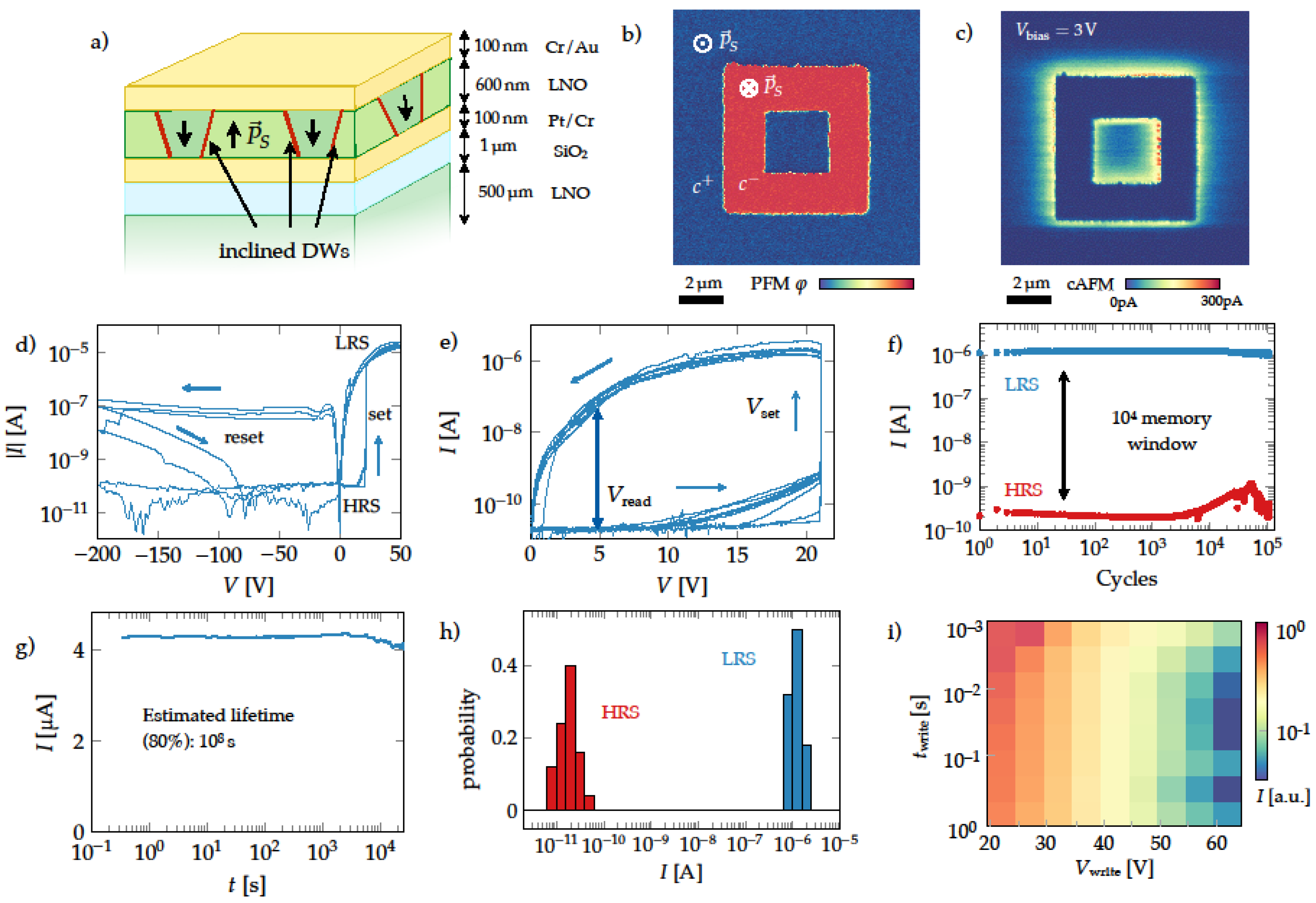
We investigated single-crystalline congruent thin-film lithium niobate, displaying a single ferroelectric domain after preparation. The samples were fabricated by a modified ion-slicing technique on 6” wafers [27]. Within the process, a platinum electrode is deposited onto the handling wafer before the wafer bonding. The thickness of the layer was set to be 600 nm by chemical-mechanical polishing and checked by ellipsometry. This enables electrical read-out, yet still preserving the single-crystalline and single domain configuration. High-resolution XRD measurements confirmed the high quality of the films oriented along (001). Electrodes with sizes of A ≈ 20,000 μm2, consisting of Cr/Au with a thickness of 100 nm, were evaporated and lithographically structured to enable the electrical characterization.
The bare film was further investigated by scanning probe microscopy to identify the formation of conductive DWs. Hereby, full-metal Pt AFM tips were applied. The domain patterns were written at a constant voltage of 65 V. To identify the locally written domain pattern we used piezo-response force microscopy (PFM). Conductive AFM (cAFM) was performed at bias voltages up to 10 V.
The local I–V-curves reveal a strong unipolar conductance, which enables erasing the conductive domain walls by applying an external counter-bias. We investigated whether a similar conductive DW formation is possible in a parallel plate capacitor structure using homogeneous electrodes. Hence, we deposited Cr/Au electrodes with a size of A ≈ 20,000 μm2 and a thickness of 100 nm on a LNO film with a thickness of 600 nm and Ti/Pt back electrode.
3. Results
3.1. Conductive AFM Investigation
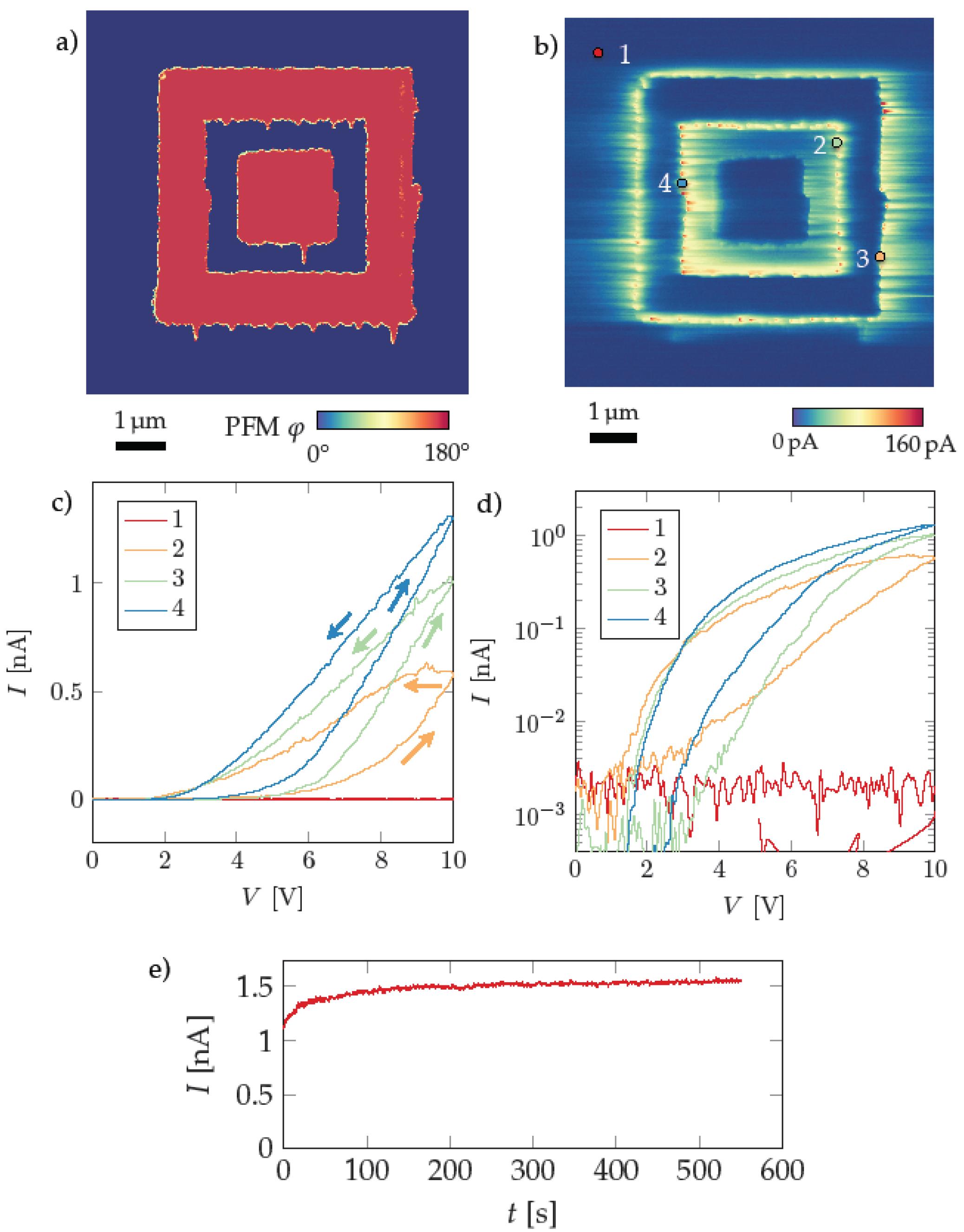
DWs were probed by cAFM to investigate the emergence of DW conductivity in these congruent LNO films. In Figure 1a,b a comparison of piezoresponse force microscopy (PFM) and subsequent cAFM measurements is given on the previously created domain pattern, which reveals a perfect match between the derived DWs from PFM and the conductive areas in the films. To further explore the conduction properties of CDWs in LNO thin films, local I–V measurements were carried out. The local current detected for a range of bias voltages is given in Figure 1c,d. Spot 1 is taken as reference and shows only a slight increase in conductivity over as long as about 500s at a voltage of 10 V (<10−2 nA). At the DW position, however, there is a strong nonlinear increase in current with applied voltage. At all points, a significant increase over several orders of magnitude (at least three) can be observed, which sufficiently separates these states from the background. The temporal stability measurements show a small increase in current over time. An example is given in Figure 1e. Local probe measurements on these CDWs reveal a stable conductance after 3 h with a minute increase over the measurement of 5% between 1 h and 3 h, hence influences by drift can be ruled out for the given shorter-term measurement.
3.2. Phase-Field Simulation
The formation of inclined DWs is generally encountered as the reason for conductive DWs in LNO. Yet, the stable formation of such inclined DWs is still a topic of current research. We applied phase field simulations, as they can provide further evidence for the existence and stability of CDWs in ferroelectric thin films. Phase field simulations have been used to study the domain pattern formation in many proper ferroelectrics, including BTO, BFO, and PZT [28]. In this study, we have modeled the temporal evolution of ferroelectric domains in LNO thin films in response to the electrical field created by a biased probe tip. In the simulations, the voltage is ramped up to a given bias voltage. A domain nucleus is formed (shown in Figure 2a), which grows into the single-crystalline film. Due to the external bias field, canted polarization states with in-plane polarization components are created. Afterwards, the inverted domain reaches the rear surface and grows sideways until an equilibrium is reached. When the bias voltage is released, the switched domain relaxes. We observe a stable CDW formation with a non-zero inclination angle, dependent on the maximum bias voltage applied. Since the gradient energy coefficients, which determine the DW width and energy, are rarely reported for LNO, we use the value estimated by Scrymgeour et al. [29]. We notice that increasing the gradient coefficients leads to a disappearance of the DW inclination, suggesting that the stability of inclined DWs in LNO may be attributed to its relatively small gradient energy.
The gradient coefficients of uniaxial LNO and LTO are significantly smaller than for other perovskite ferroelectrics. Previous reports on 180°DW conductance in ferroelectric thin films supports our conjecture. For example, the reported DW inclination in as-poled LTO bulk material was apparently larger [15,30]. Still, it has to be noted that the coefficients are not well known and effects from gradient energy anisotropy and carrier generation could be significant.
The evolution in DW inclination for various tip voltages is given for films of a thickness of 20 nm and 50 nm in Figure 2b,c. In all given cases, a non-zero inclination can be observed after the external bias field is completely removed. The extracted final inclination angle is plotted over the homogenized applied external field. We can observe a decrease in inclination with larger applied external field. A similar behavior in the extracted DW conductance can prove a link between the degree of inclination of a DW and its conductance. To compare the theoretical prediction with the experimental condition, domains were written with a domain size of d = 500 nm at various tip voltages. The written domains are visualized by PFM in Figure 2e. The conductivity extracted by cAFM shows a decrease in current for larger applied writing voltage. In Figure 2f the extracted maximum current values at the DW are given. A similar behavior of the current as a function of the simulated inclination angle can be observed. This is in agreement with previous theoretical assumptions [8] that the DW conductance of inclined DWs is proportional to its inclination and follows σ = 2PS sin α.
3.3. Resistive Switching Investigations
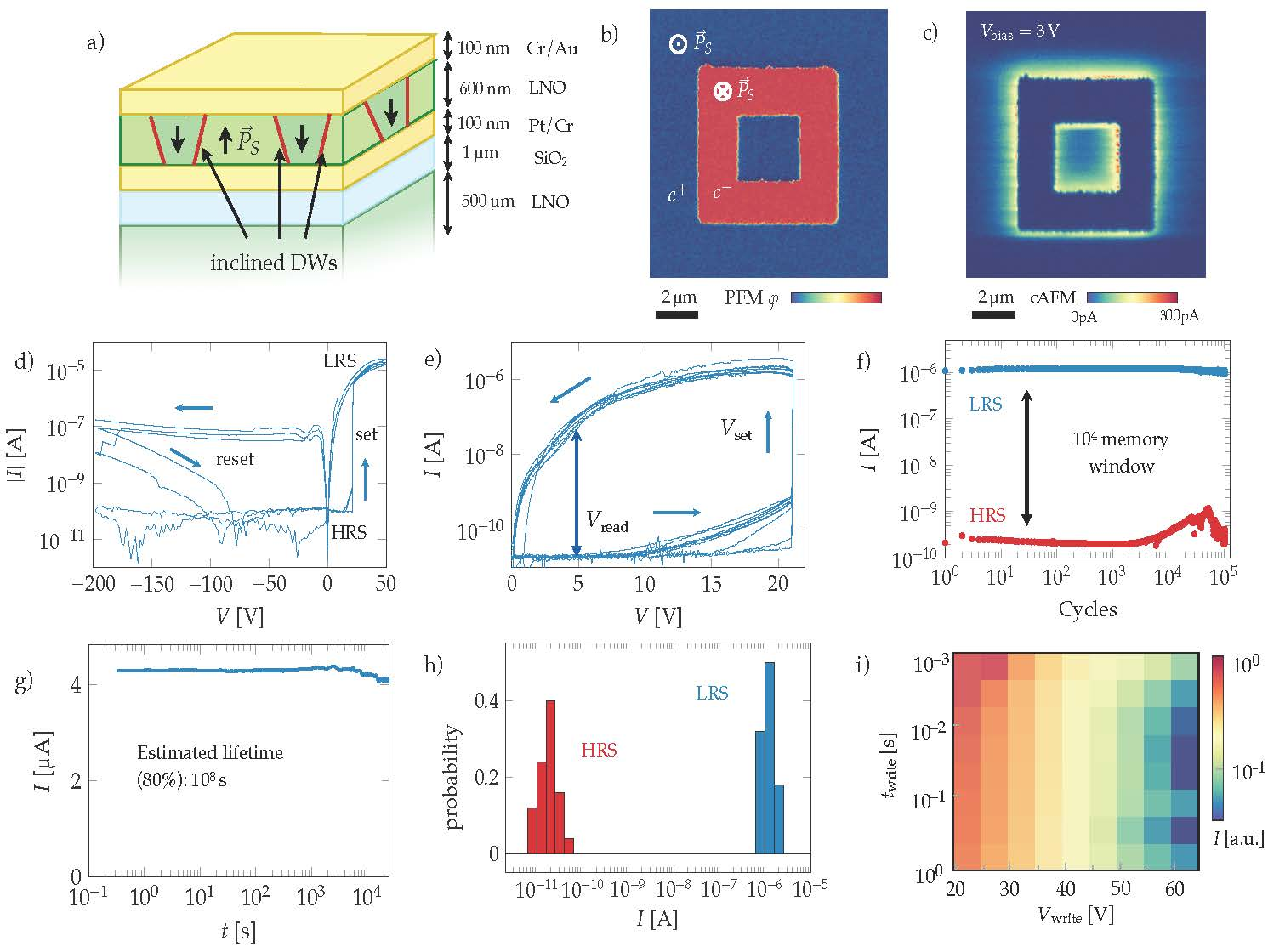
To further analyze the properties of the conductance, I–V measurements were conducted in plate-electrode condition, schematically sketched in Figure 3a under the assumption of inclined domain wall generation at nucleus sites, which would result in strong conductance changes upon reach of the local coercive voltage. Indeed, we can observe a very strong increase over five orders of magnitude in current at a very defined set voltage Vset = 21.05 V with an accuracy of ∆Vset/Vset = 10−3, which is proven to be the local coercive voltage from PFM measurements. This value of Vset is not only reproduced for a single device, but also for 50 individual devices on a single wafer, which clearly underlines the very precise and reproducible behavior of single-crystalline resistive switching devices. Up to a voltage of −3 V, a very symmetric current–voltage relation can be observed. Yet, for larger negative biases, the absolute value of the current saturates and is not stable anymore but reduces with time. The given cycles in Figure 3d are obtained with a cycle frequency of 1.5 mHz. The observed behavior is very similar to back-switching observed upon current injection from the top electrode at small voltages confirmed by PFM. Hence, we suppose, upon the application of a negative bias, insulating straight or tail-to-tail DWs are formed or domain inversion is invoked; thus, there is no complete conductive channel anymore, which prohibits a current flow.
Before switching the resistance state, one can observe no current larger than 10 pA, which is the lower limit for current detection of the applied source-meter. Further measurements with a further electrometer revealed an even smaller upper current limit of 200 fA at a voltage of −200 V, which corresponds to a resistance of at least 1 PΩ up to a bias voltage of −200 V or an electric field of 3.4 MV/cm, which underlines that leakage is negligible in the films. This similarly holds for positive read-out voltages in the high resistance state (HRS). Hence, the HRS is expected to have a resistance of at least 25 TΩ, with the low resistance state at around 10 MΩ; hence, we observe a huge resistance change over seven orders of magnitude. By setting the switch, no overshoot is present; thus the HRS setting is self-limiting. In Figure 3e the half cycle I–V-curves are shown upon the boundary condition, the current having reduced to 10−8 A at −210 V. We can observe the reproducible set voltage. However, below this specific voltage, a slight increase in current can be observed. In general, this current, which deviates from the first cycle, is smaller the lower the current at V = −210 V. It saturates after several cycles. Several reasons are possible, e.g., deep traps, which are incorporated into the film upon large current flow. Hence, for endurance testing high voltage treatment was kept as short as possible. In Figure 3f the endurance upon such cycling is shown. The resistance is measured after every cycle. The LRS is created on application of Vset = 21.1 V. The system is released into the HRS upon application of V = −210 V. This results in a very enduring resistive switching device over at least 105 cycles. The states can be read out without destruction. The temporal stability of the LRS is given in Figure 3g. As is visible, the conductance is very stable over at least 104 s. Hence, assuming an exponential decrease and a minimum current of 80%, a stability over 108 s or 10 years can be predicted. Similar measurements with an AFM tip revealed the stability of the current on CDWs over at least 3 h, which is about the longest time to measure due to probe drift. The statistical results given in Figure 3h show a sufficiently high margin for the application as a nonvolatile memory.
Under the application of larger set voltages and shorter pulses being applied among domain formation, the domain wall is expected to straighten, which would result in a decrease in conductance. Indeed, this can be seen as given in Figure 3i. Particularly, the fact that stronger applied electric fields result in reduced conductivity is very unusual and supports the conductance measured to be derived by inclined domain walls.
This proof of high endurance, high on/off current switching, high retention and the tenability among programming makes charged domain walls an interesting tunable nonvolatile memory.
3.4. Conductance Type Extraction
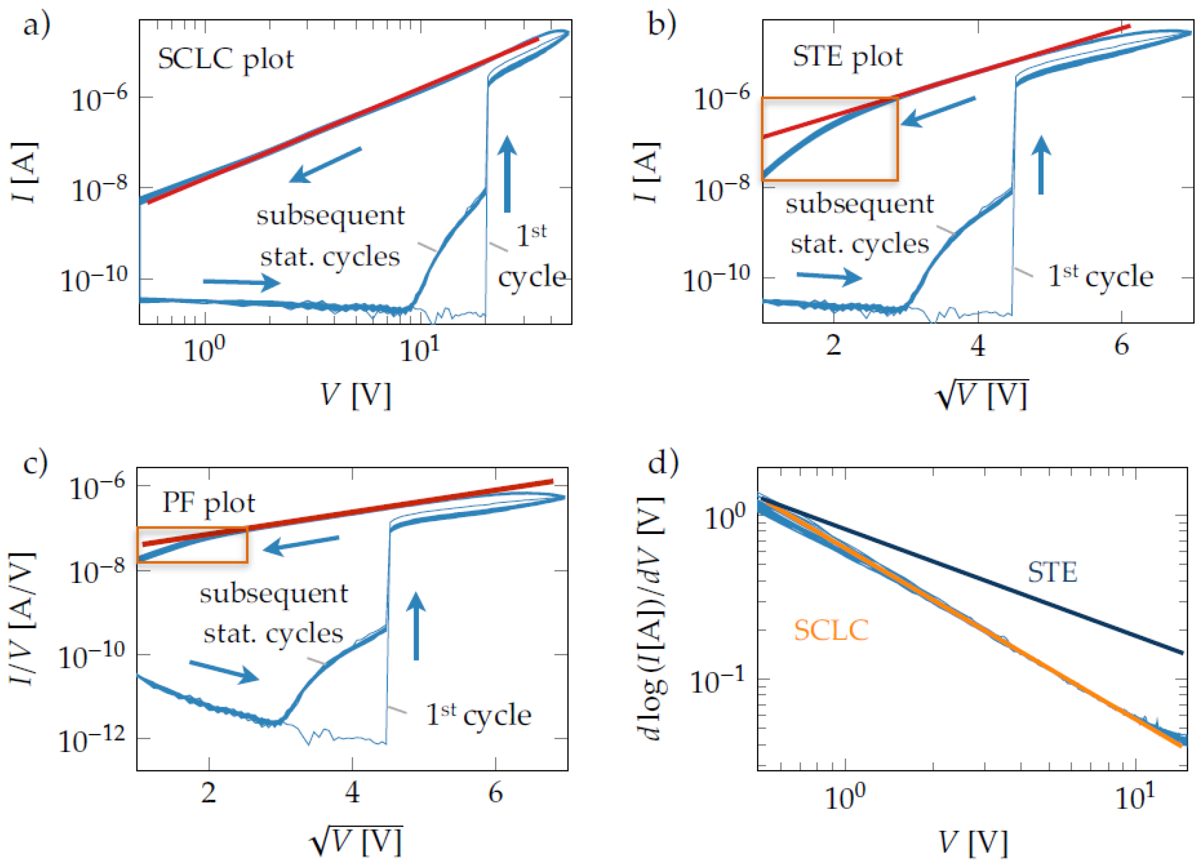
The conduction type was investigated by I–V measurements by linearization with typical mechanisms. In Figure 4a, the I–V measurements are plotted according to space-charge-limited current (SCLC) theory, which predicts I∼V2 in a log–log plot. A fit is given, which shows a perfect fit over almost two voltage magnitudes. In Figure 4b the I–V curve is linearized according to Shottky thermioninc emission (STE). A good fit can be seen in a medium voltage range, but both for a small and large voltage significant deviations are visible. Similarly, in the case of Poole–Frenkel (PF) linearization given in Figure 4c, we obtain a reasonable fit for medium voltages, but discrepancies for very low and high voltages. Yet, it would be not sufficient to formally exclude these two transport mechanisms. Likewise, the linearization with Fowler–Nordheim (FN) tunneling does not give a decent fit. In the LRS we obtain a flat line. Hence, the first three transport mechanisms still have to be considered. Thus, we used the abrupt junction approximation, which assumes a pn-junction with an abrupt doping profile [31] Even though the main advantage of this method is to understand impedance upon a DC bias, it is still helpful to analyze the plain DC I–V curves as dlog(I)/dV is independent on most parameters, especially the contact area; it is, hence, more robust, especially upon temperature changes, and it is possible to differentiate between FN and PF. Hence, in Figure 4d, the I–V curves in a temperature range T between 300 K and 340 K are given. Only SCLC and PF [both dlog(I)/dV ∼ V−1] can describe such a curve, whereas STE [dlog(I)/dV ∼ V−3/4] cannot describe this behavior. Yet, in the case of PF, a very strong component ∝ V−1/2 should also be present, which cannot be seen in the measurements. The I–V SCLC curve fit is almost perfect over two orders of magnitude and, thus, significantly better than those of PF and STE.
So far, we have solely discussed electronic transport. Yet, especially, resistive switching is generally an interplay of both ionic and electronic current contributions. Hence, it is necessary to further rule out scenarios of mixed electronic–ionic conduction. We use the Nernst–Ernstein equation to analyze whether ionic conduction is a significant contribution, which is given by ∆ = τeDE/kT, with τ the diffusion time and D the diffusion constant. Using a conservative value of D ∼ 10−18 m2/s, which is derived from experimental values of lithium transport in LixSi [32], the estimated ionic movement over 100 ms is about ∼0.8 nm at a field of 2 × 10⁷ V/m and room temperature T = 300 K, which is about three orders of magnitude smaller than the film thickness. Reported values for the ionic transport diffusion constants in LNO (e.g., Li, H, D, Na, Mg) at elevated temperatures and interpolated to room temperature are significantly smaller. Hence, we can exclude ionic current having a major share.
The conduction in DWs, thus, follows the Mott–Gurney equation (Child’s law) [33]: I(T) = Aeff 9εμ(T)V2/8d3 with Aeff the effective contact area, d the thickness of the dielectric film, ε the static permittivity, and μ(T) the mobility of the major charge carrier. Using the current extracted from cAFM measurements, we can derive a mobility of about 5 ± 3 × 10⁻² cm2/Vs, which is in good agreement with previously reported macroscopic photo-induced current measurements [34]. The temperature dependence in an SCLC transport regime is solely determined by the temperature dependence of the mobility of the major charge carrier.
3.5. Temperature Dependent Conductance
The temperature dependence of the conductance in the Au/Cr/LNO/Pt stack is given in Figure 5. We observe three current regimes. In ①, for temperatures above 300 K, an activation energy of 0.63 eV was obtained; in ②, between 300 K and about 100 K, we obtain an activation energy of 0.18 eV. For temperatures below 100 K ③, we obtain an activation energy of only 0.03 eV. Very similar regimes have been proposed very recently for the lifetime of bound polaron in lightly-doped Fe:LNO via Monte-Carlo simulations [35].
The processes which are assigned to these three regimes are given as:
① NbLi4+ + NbNb5+ → NbLi5+ + NbNb4+, Ea ∼ 0.65 eV
② NbLi4+ + NbLi5+ → NbLi5+ + NbLi4+, Ea ∼ 0.2 eV
③ NbLi4+ + FeLi3+ → NbLi5+ + FeLi2+, Ea ∼ 0.03 eV.
The simulated bound polaron lifetime by Mhaouech and Guilbert is overlaid on the aforementioned temperature-dependent I–V curves given in Figure 5.
Thus, we can conclude that the current through the exfoliated LNO thin film is mainly governed by an interplay of bound and free small polaron transport, depending on the given temperature. As iron impurities act as deep traps, they will inhibit any further conduction. The hopping activation energy of Fe2+ is given to be 0.35 eV [36], hence, only a little larger than Li for bound and free polarons, but as the hopping rate follows w ∼ e−r/a ≈ e−r[Å], hopping transport is very unlikely for the given concentrations and even for lightly doped Fe:LNO not relevant. A conversion to bound and small polarons is unlikely due to the high binding energy of 1.22 eV.
4. Discussion and Conclusions
In this study, we reported the domain wall conductance by inclined domain walls in LNO thin films, which could be applied as a new multi-level non-volatile memory cell based on out-of-plane ferroelectric switching, by the precise tuning of the inclination and thus the conductance state. We investigated further the temperature dependence as well as the temporal dependence on erase voltage application and concluded that the main contribution to the current is space-charge-limited.
We obtained evidence the current to be dominated by a polaron gas formation at such inclined domain wall and confined by the band bending from the temperature dependence of the conductance. Upon local inversion, generally, charge carrier injection is discussed, even though it has been speculative for a long time. Assuming such charge carriers are injected at the DW, which are needed to compensate the inclined DW of the spike-domain-like nucleus, free charge carriers—electrons—are generated, which will condensate into similarly charged and, hence, screening electron polaronic, states inside the single crystal material. Such a transition has been observed in bulk material, e.g., by optical time-resolved spectroscopy, to happen within 200 fs [37]. Yet, at a CDW these values can be significantly larger due to the smaller energy gap between conductance band and Fermi energy. However, as the band-bending is not large enough to create a 2DEG, which would be apparent with much higher mobility conductivity, we assume a 2D polaron gas (2DPG) is obtained. Bound polarons will very rapidly be trapped by iron impurities. Upon pure-diffusion transport, thus without an external electric field, the average mean free path of the bound polaron until trapping with FeLi is < tNbLi4+ ≥ 100 Å and for the free polaron is < tNbNb4+ ≥ 80 Å. These values were derived by interpolation from the data of Mhaouech and Guilbert [35] under consideration of the smaller iron impurity concentration cFe = 1017 cm−3 and a niobium antisite defect concentration of cNbLi = 1021 cm−3. Upon drift condition, these values can be larger. Hence, the bound polaron has a larger mean free path. However, the hopping rate of bound polarons is only wNbLi4+ = 107 s−1. Assuming the hopping rate to depend mainly on the nearest neighbor distance, like w~er[Å], we can calculate, that the hopping rate of free polarons is two orders of magnitude larger, hence wNbLi4+ = 109 s−1. Thus, the electric current with free polaron transport as in Mg:LNO can be significantly larger. This again explains why, for the case of bulk material only, congruent Mg:LNO revealed a conductance upon UV illumination. For the ultrathin LNO films in use in this study, even undoped material can give measureable conductance.
The model explains why an asymmetric electrode condition can result in the efficient switching between an HRS and LRS. Upon the negative pulse application, the carrier density reduces, which destabilizes the inclined domain wall formation and finally reduces the conductance of the wall further. However, this process requires relatively high electric fields and times due to the low mobility of the charge carriers. Hence, the study suggests that Mg:LNO and thinner films can significantly improve the performance of the tunable non-volatile memory.
The thin-film lithium niobate resistive switching effect based on charged ferroelectric domain walls formation and erasure offers interesting advantages over conventional filament-based resistive switching, which can be interesting for neuromorphic computing applications.
Author Contributions
Investigation, T.K., B.W.; resources, A.H., L.M.E.; writing—review and editing, T.K.; supervision, L.-Q.C., L.M.E. All authors have read and agreed to the published version of the manuscript.
Funding
This research was funded by the Cluster of Excellence “Center of Advancing Electronics Dresden” and the DFG Research Grant HA 6982/1-1. We also acknowledge open access funding support by the publication fund of TU Dresden.
Acknowledgments
The authors would like to acknowledge the support of NanoLN for the provision of the lithium niobate thin film samples, H. Hui (Shandong University) for helpful discussions, and S. Johnston as well as Z.X. Shen (Stanford) for measurement support. B.W. acknowledges the support by the NSF-MRSEC grant number DMR-1420620. The effort of L.-Q.C. is supported by National Science Foundation (NSF) through Grant No. DMR-1744213.
Conflicts of Interest
The authors declare no conflict of interest.
References
- Seidel, J.; Martin, L.W.; He, Q.; Zhan, Q.; Chu, Y.-H.; Rother, A.; Hawkridge, M.E.; Maksymovych, P.; Yu, P.; Gajek, M.; et al. Conduction at domain walls in oxide multiferroics. Nat. Mater. 2009, 8, 229–234. [Google Scholar] [CrossRef] [PubMed] [Green Version]
- Guyonnet, J.; Gaponenko, I.; Gariglio, S.; Paruch, P. Conduction at domain walls in insulating Pb (Zr0.2Ti0.8)O3 thin films. Adv. Mater. 2011, 23, 5377. [Google Scholar] [CrossRef] [PubMed] [Green Version]
- Gaponenko, I.; Tückmantel, P.; Karthik, J.; Martin, L.W.; Paruch, P. Towards reversible control of domain wall conduction in Pb (Zr0.2Ti0.8)O3 thin films. Appl. Phys. Lett. 2015, 106, 162902. [Google Scholar] [CrossRef] [Green Version]
- Lu, H.; Tan, Y.; McConville, J.P.V.; Ahmadi, Z.; Wang, B.; Conroy, M.; Moore, K.; Bangert, U.; Shield, J.E.; Chen, L.-Q.; et al. Electrical Tunability of Domain Wall Conductivity in LiNbO3 Thin Films. Adv. Mater. 2019, 31, 1902890. [Google Scholar] [CrossRef]
- Volk, T.R.; Gainutdinov, R.V.; Zhang, H.H. Domain-wall conduction in AFM-written domain patterns in ion-sliced LiNbO3 films. Appl. Phys. Lett. 2017, 110, 132905. [Google Scholar] [CrossRef]
- Rojac, T.; Bencan, A.; Drazic, G.; Sakamoto, N.; Ursic, H.; Jancar, B.; Tavcar, G.; Makarovic, M.; Walker, J.; Malic, B.; et al. Domain-wall conduction in ferroelectric BiFeO3 controlled by accumulation of charged defects. Nat. Mater. 2017, 16, 322–327. [Google Scholar] [CrossRef]
- Eliseev, E.A.; Morozovska, A.N.; Svechnikov, G.S.; Gopalan, V.; Shur, V.Y. Static conductivity of charged domain walls in uniaxial ferroelectric semiconductors. Phys. Rev. B 2011, 83, 235313. [Google Scholar] [CrossRef] [Green Version]
- Xiao, S.Y.; Kämpfe, T.; Jin, Y.M.; Haußmann, A.; Lu, X.M.; Eng, L.M. Dipole-Tunneling Model from Asymmetric Domain-Wall Conductivity in LiNbO3 Single Crystals. Phys. Rev. Appl. 2018, 10, 034002. [Google Scholar] [CrossRef]
- Sturman, B.; Podivilov, E.; Stepanov, M.; Tagantsev, A.; Setter, N. Quantum properties of charged ferroelectric domain walls. Phys. Rev. B 2015, 92, 21. [Google Scholar] [CrossRef]
- Godau, C.; Kämpfe, T.; Thiessen, A.; Eng, L.M.; Haußmann, A. Enhancing the domain wall conductivity in lithium niobate single crystals. ACS Nano 2017, 11, 5. [Google Scholar]
- Werner, C.S.; Herr, S.J.; Buse, K.; Sturman, B.; Soergel, E.; Razzaghi, C.; Breunig, I. Large and accessible conductivity of charged domain walls in lithium niobate. Sci. Rep. 2017, 7, 9862. [Google Scholar] [CrossRef] [PubMed]
- Pawlik, A.-S.; Kämpfe, T.; Haußmann, A.; Woike, T.; Treske, U.; Knupfer, M.; Büchner, B.; Soergel, E.; Streubel, R.; Koitzsch, A.; et al. Polarization driven conductance variations at charged ferroelectric domain walls. Nanoscale 2017, 9, 30. [Google Scholar] [CrossRef] [PubMed]
- Kirbus, B.; Godau, C.; Wehmeier, L.; Beccard, H.; Beyreuther, E.; Haußmann, A.; Eng, L.M. Real-Time 3D Imaging of Nanoscale Ferroelectric Domain Wall Dynamics in Lithium Niobate Single Crystals under Electric Stimuli: Implications for Domain-Wall-Based Nanoelectronic Devices. ACS Appl. Nanomater. 2019, 2, 5787–5794. [Google Scholar] [CrossRef]
- Xia, Q.; Yang, J.J. Memristive crossbar arrays for brain-inspired computing. Nat. Mater. 2019, 18, 309–323. [Google Scholar] [CrossRef] [PubMed]
- Schröder, M.; Haußmann, A.; Thiessen, A.; Soergel, E.; Woike, T.; Eng, L.M. Conducting domain walls in lithium niobate single crystals. Adv. Funct. Mater. 2012, 22, 3936. [Google Scholar] [CrossRef]
- Schröder, M.; Chen, X.; Haußmann, A.; Thiessen, A.; Poppe, J.; Bonnell, D.A.; Eng, L.M. Nanoscale and macroscopic electrical ac transport along conductive domain walls in lithium niobate single crystals. Mater. Res. Express 2014, 1, 035012. [Google Scholar] [CrossRef]
- Kämpfe, T.; Reichenbach, P.; Schröder, M.; Haußmann, A.; Eng, L.M.; Woike, T.; Soergel, E. Optical three-dimensional profiling of charged domain walls in ferroelectrics by Cherenkov second-harmonic generation. Phys. Rev. B 2014, 89, 035314. [Google Scholar] [CrossRef]
- Kämpfe, T.; Reichenbach, P.; Haußmann, A.; Woike, T.; Soergel, E.; Eng, L.M. Real-time three-dimensional profiling of ferroelectric domain walls. Appl. Phys. Lett. 2015, 107, 152905. [Google Scholar] [CrossRef]
- Wehmeier, L.; Kämpfe, T.; Haußmann, A.; Eng, L.M. In situ 3D observation of the domain wall dynamics in a triglycine sulfate single crystal upon ferroelectric phase transitio. Phys. Stat. Solidi RRL 2017, 11, 1700267. [Google Scholar] [CrossRef]
- Reichenbach, P.; Kämpfe, T.; Thiessen, A.; Haußmann, A.; Woike, T.; Eng, L.M. Multiphoton photoluminescence contrast in switched Mg: LiNbO3 and Mg: LiTaO3 single crystals. Appl. Phys. Lett. 2014, 105, 22906. [Google Scholar] [CrossRef]
- Reichenbach, P.; Kämpfe, T.; Thiessen, A.; Schröder, M.; Haußmann, A.; Woike, T.; Eng, L.M. Conducting domain walls in lithium niobate single crystals. J. Appl. Phys. 2014, 115, 213509. [Google Scholar] [CrossRef]
- Reichenbach, P.; Kämpfe, T.; Haußmann, A.; Thiessen, A.; Woike, T.; Steudtner, R.; Kocsor, L.; Szaller, Z.; Kovács, L.; Eng, L.M. Polaron-Mediated Luminescence in Lithium Niobate and Lithium Tantalate and Its Domain Contrast. Crystals 2018, 8, 214. [Google Scholar] [CrossRef] [Green Version]
- Haußmann, A.; Kirsten, L.; Schmidt, S.; Cimalla, P.; Wehmeier, L.; Koch, E.; Eng, L.M. Three-Dimensional, Time-Resolved Profiling of Ferroelectric Domain Wall Dynamics by Spectral-Domain Optical Coherence Tomography. Ann. Phys. 2017, 529, 1700139. [Google Scholar] [CrossRef]
- Haußmann, A.; Gemeinhardt, A.; Schröder, M.; Kämpfe, T.; Eng, L.M. Bottom-up assembly of molecular nanostructures by means of ferroelectric lithography. Langmuir 2017, 33, 475–484. [Google Scholar] [CrossRef]
- Gonnissen, J.; Batuk, D.; Nataf, G.F.; Jones, L.; Abakumov, A.M.; van Aert, S.; Schryvers, D.; Salje, E.K.H. Direct Observation of Ferroelectric Domain Walls in LiNbO3: Wall-Meanders, Kinks, and Local Electric Charges. Adv. Funct. Mater. 2016, 26, 42. [Google Scholar] [CrossRef]
- Conroy, M.; Moore, K.; O’Connell, E.N.; McConville, J.P.V.; Lu, H.; Chaudhary, P.; Lipatov, A.; Sinitskii, A.; Gruverman, A.; Gregg, J.M.; et al. Atomic-Scale Characterization of Ferro-Electric Domains in Lithium Niobate-revealing the Electronic Properties of Domain Wall. Microsc. Microanal. 2019, 25, 576–577. [Google Scholar] [CrossRef] [Green Version]
- Poberaj, G.; Hu, H.; Sohler, W.; Günter, P. Lithium niobate on insulator (LNOI) for micro-photonic devices. Laser Photonics Rev. 2012, 6, 488–503. [Google Scholar] [CrossRef]
- Chen, L.Q. Phase-field models for microstructure evolution. Ann. Rev. Mat. Res. 2002, 32, 113–140. [Google Scholar] [CrossRef] [Green Version]
- Scrymgeour, D.; Gopalan, V.; Itagi, A.; Saxena, A.; Swart, P. Phenomenological theory of a single domain wall in uniaxial trigonal ferroelectrics: Lithium niobate and lithium tantalite. Phys. Rev. B 2005, 71, 184110. [Google Scholar] [CrossRef] [Green Version]
- Kämpfe, T. Charged Domain Walls in Ferroelectric Single Crystals. Ph.D. Thesis, Dresden University of Technology, Dresden, Germany, 2017. [Google Scholar]
- Maksymovych, P.; Pan, M.; Yu, P.; Ramesh, R.; Baddorf, A.P.; Kalinin, S.V. Scaling and disorder analysis of local I–V curves from ferroelectric thin films of lead zirconate titanate. Nanotechnology 2011, 22, 254031. [Google Scholar] [CrossRef]
- Ding, N.; Xu, J.; Yao, Y.X.; Wegner, G.; Fang, X.; Chen, C.H.; Lieberwirth, I. Determination of the diffusion coefficient of lithium ions in nano-Si. Solid State Ion. 2009, 180, 222–225. [Google Scholar] [CrossRef]
- Mott, N.F.; Gurney, R.W. Electronic Processes in Ionic Crystals; The Clarendon Press: Oxford, UK, 1940. [Google Scholar]
- Kämpfe, T.; Haußmann, A.; Eng, L.M.; Reichenbach, P.; Thiessen, A.; Woike, T.; Steudtner, R. Time-resolved photoluminescence spectroscopy of Nb Nb 4+ and O− polarons in LiNbO3 single crystals. Phys. Rev. B 2016, 93, 74116. [Google Scholar] [CrossRef]
- Mhaouech, I.; Guilbert, L. Temperature dependence of small polaron population decays in iron-doped lithium niobate by Monte Carlo simulations. Solid State Sci. 2016, 60, 28–36. [Google Scholar] [CrossRef]
- Sanson, A.; Zaltron, A.; Argiolas, N.; Sada, C.; Bazzan, M.; Schmidt, W.G.; Sanna, S. Polaronic deformation at the Fe2+/3+ impurity site in Fe: LiNbO3 crystals. Phys. Rev. B 2015, 91, 094109. [Google Scholar] [CrossRef]
- Schirmer, O.F.; Imlau, M.; Merschjann, C.; Schoke, B. Electron small polarons and bipolarons in LiNbO3. J Phys. Cond. Matter 2009, 21, 23201. [Google Scholar] [CrossRef]
Figure 1.
DW conductance in the congruent LNO thin films: (a) domain configuration by PFM; (b) cAFM scan at a bias voltage of 3 V; (c) Local I–V measurements on conductive DWs at four marked spots; (d) logarithmic plot of the detected current; (e) temporal development of the current at spot 4 at an external bias voltage of 10 V.

Figure 2.
(a) Three-dimensional phase field simulation of CDW formation under an AFM tip for a 20 nm thick lm at 20 V. ① Nucleation, ② through domain formation until equilibrium under external bias, ③ equilibrium domain after removal of bias. (b,c) evolution of inclination angle for film thicknesses, d, of 50 nm and 20 nm respectively; (d) equilibrium inclination angle after removal of bias as a function of applied field; (e) measured current Iread at a bias voltage of 10 V for domains written at various writing voltages Vwrite, for comparison PFM scans; (f) extracted maximum domain wall current.

Figure 3.
Investigation of the switching behavior, endurance, stability, and tunability of resistive switching of the Pt/LNO/Cr/Au stack with a contact area of 2000 μm2. (a) film stack configuration (b) PFM scan of a written domain (c) cAFM scan at a bias voltage of 3V; (d) full I-V cycle (f = 1.5 mHz) with a very defined set voltage Vset = 21.05 V (DVset/Vset~10−3), hence a comparably small electric field Eswitch,off = 0.3 MV/cm and strongly rectifying behavior without significant leakage upon an electric field of Eswitch,off = 3.4 MV/cm with a resistance of >20 TW, (e) switch-on I-V cycle with constant switch-off voltage Vswitch,off = −210 V, (f) endurance of high resistance and low-resistance state (HRS, LRS, respectively) over at least 105 cycles with a resistance window of >104 and a read voltage of 10 V, (g) time stability of low resistant state over 104 s, which yields an 80% reliability over 108 s or 3 years, (h) probability of the current in HRS and LRS at 10 V for 50 tested devices on the same single crystalline thin-film (i) tunability of readout current Iread,on under modulation of writing time twrite and writing voltage Vwrite. The read-out current Iread,on reduces for larger writing voltages Vwrite,on. Iread,on is the average value over 100 writing cycles each.

Figure 4.
Conductance type analysis on CDWs in LNO (a) SCLC I–V plot; (b) STE I–V plot; (c) PF I–V plot; (d) derivative plot. The I–V curves show the first cycle and the stationary cycles after 20 cycles. The off-state was obtained by applying V = −210 V until the current is reduced to 10−8 A.
Figure 4.
Conductance type analysis on CDWs in LNO (a) SCLC I–V plot; (b) STE I–V plot; (c) PF I–V plot; (d) derivative plot. The I–V curves show the first cycle and the stationary cycles after 20 cycles. The off-state was obtained by applying V = −210 V until the current is reduced to 10−8 A.

Figure 5.
Temperature dependence of the current for thin-film LNO. Measured current at different voltages from 360 K to 77 K. We can observe different regimes of thermal activation ① above 300 K with Ea = 0.63 eV, at ② between 300 K and 100 K with Ea = 0.18 eV and ③ below 100 K with a thermal activation of Ea = 0.03 eV. These are overlaid with the inverse bound polaron lifetime, as calculated by Monte Carlo (MC) simulations.

© 2020 by the authors. Licensee MDPI, Basel, Switzerland. This article is an open access article distributed under the terms and conditions of the Creative Commons Attribution (CC BY) license (http://creativecommons.org/licenses/by/4.0/).
Share and Cite
MDPI and ACS Style
Kämpfe, T.; Wang, B.; Haußmann, A.; Chen, L.-Q.; Eng, L.M. Tunable Non-Volatile Memory by Conductive Ferroelectric Domain Walls in Lithium Niobate Thin Films. Crystals 2020, 10, 804. https://0-doi-org.brum.beds.ac.uk/10.3390/cryst10090804
AMA Style
Kämpfe T, Wang B, Haußmann A, Chen L-Q, Eng LM. Tunable Non-Volatile Memory by Conductive Ferroelectric Domain Walls in Lithium Niobate Thin Films. Crystals. 2020; 10(9):804. https://0-doi-org.brum.beds.ac.uk/10.3390/cryst10090804
Chicago/Turabian StyleKämpfe, Thomas, Bo Wang, Alexander Haußmann, Long-Qing Chen, and Lukas M. Eng. 2020. "Tunable Non-Volatile Memory by Conductive Ferroelectric Domain Walls in Lithium Niobate Thin Films" Crystals 10, no. 9: 804. https://0-doi-org.brum.beds.ac.uk/10.3390/cryst10090804
Note that from the first issue of 2016, this journal uses article numbers instead of page numbers. See further details here.