Article

Depth Profile Analysis of Deep Level Defects in 4H-SiC Introduced by Radiation

1
Ruđer Bošković Institute, Bijenička 54, 10000 Zagreb, Croatia
2
Takasaki Advanced Radiation Research Institute, National Institutes for Quantum and Radiological Science and Technology, 1233 Watanuki, Takasaki, Gunma 370-1292, Japan
3
Jozef Stefan Institute, Jamova 39, 1000 Ljubljana, Slovenia
4
Australian Nuclear Science and Technology Organisation, 1New Illawarra Rd, Lucas Heights, NSW 2234, Australia
*
Author to whom correspondence should be addressed.
Submission received: 1 September 2020 / Revised: 13 September 2020 / Accepted: 19 September 2020 / Published: 22 September 2020
(This article belongs to the Special Issue Crystalline Materials for Radiation Detection: A New Perspectives)

Abstract

:
Deep level defects created by implantation of light-helium and medium heavy carbon ions in the single ion regime and neutron irradiation in n-type 4H-SiC are characterized by the DLTS technique. Two deep levels with energies 0.4 eV (EH1) and 0.7 eV (EH3) below the conduction band minimum are created in either ion implanted and neutron irradiated material beside carbon vacancies (Z1/2). In our study, we analyze components of EH1 and EH3 deep levels based on their concentration depth profiles, in addition to (−3/=) and (=/−) transition levels of silicon vacancy. A higher EH3 deep level concentration compared to the EH1 deep level concentration and a slight shift of the EH3 concentration depth profile to larger depths indicate that an additional deep level contributes to the DLTS signal of the EH3 deep level, most probably the defect complex involving interstitials. We report on the introduction of metastable M-center by light/medium heavy ion implantation and neutron irradiation, previously reported in cases of proton and electron irradiation. Contribution of M-center to the EH1 concentration profile is presented.

1. Introduction

Silicon carbide (SiC) is a wide band gap semiconductor suitable for high temperature, high-frequency and high-power applications [1,2]. The 4H polytype of SiC is preferred as a material for electronic components due to the high and isotropic mobility of carriers. 4H-SiC was demonstrated as a promising material for atomic-scale spintronics and quantum applications [3,4,5]. Qubits and single-photon emitters are realized by defect engineering. A long spin-coherence time at room temperature was observed for isolated single-point defects in ion-implanted SiC such as silicon vacancy (VSi), di-vacancy, and a carbon anti-site defect [6,7,8]. Defect engineering is also used for local carrier lifetime control necessary for the optimization of the switching loss of 4H-SiC power bipolar junction transistors [9] and elimination of the bipolar degradation [10]. In recent years, 4H-SiC radiation detectors have attracted attention due to their high radiation hardness and high signal to noise ratio [11,12,13]. Electrically active defects induced by irradiation negatively affect the performance of 4H-SiC devices during their working lifetime. The characterization of irradiation introduced defects is crucial for future improvement of radiation hardness and extending the lifetime of 4H-SiC detectors.
The carbon vacancy VC is a dominant recombination center in 4H-SiC affecting the minority carrier lifetime. Therefore, the control of the minority carrier lifetime can be realized by controlling the carbon vacancy concentration [14,15,16]. The carbon vacancy concentration can be increased by using low-energy electron irradiation, which displaces only C atoms in the 4H-SiC material [17], or ion implantation [15]. On the other hand, thermal oxidation [18] or C ion implantation with subsequent annealing [19,20,21] can be used to introduce carbon interstitials into 4H-SiC, which recombine with carbon vacancies and reduce the carbon vacancy concentration. Acceptor levels of the carbon vacancy exhibit negative-U ordering [22]. Two components of the Z1/2 center were recently resolved by Laplace deep level transient spectroscopy (Laplace DLTS) and assigned to the (=/0) acceptor level of carbon vacancies residing on lattice sites with local cubic and hexagonal symmetry [23,24].
Two deep levels with energies around EC—0.4 eV and EC—0.7 eV (usually labeled as S1 and S2 or EH1 and EH3, respectively [25,26,27,28,29,30,31]) can be observed in n-type 4H-SiC after irradiation with neutrons or electrons and ion implantation. Their simultaneous appearance and correlation of their concentrations indicate that they correspond to different charge state transitions of the same defect [27]. EH1 and EH3 deep levels introduced by ion implantation have been recently assigned to VSi (−3/=) and VSi (=/−) charge transitions of the silicon vacancy [32,33], respectively. Furthermore, a metastable defect labeled as the M-center was previously observed in 4H-SiC after proton [34,35,36] and electron [37,38] irradiation. Two deep levels M1 and M3 with activation energies of 0.42 and 0.75 eV, respectively, are observed when M-center is in configuration A, while only one deep level M2 with an activation energy of 0.7 eV is detected when M-center is in configuration B [34]. Transformation of the M-center to configuration A occurs at room temperature under applied bias, while transformation to B configuration occurs at 450 K without bias. Low-energy electron irradiation (<220 keV), which displaces only carbon atoms in the 4H-SiC crystal, introduces two deep levels with activation energies 0.45 eV and 0.72 eV [39]. According to a recent study [39], they are two different transitions of the same defect related to carbon interstitials, labeled as the EH-center. The activation energy for annealing of EH-center (1.1 eV [39]) is different from the activation energy of S-center (1.8 eV [27]) and M-center (2.0 eV [37]), which indicates different defect species.
In this paper, we investigate deep level defects in n-type 4H-SiC introduced by ion implantation and neutron radiation by the DLTS and Laplace DLTS techniques. The depth profiles of the introduced deep levels are comprehensively studied, in respect to their attributions and their effect on free carrier concentration. Inspection of the depth profiles revealed an interstitially related deep level defect, which contributes to the DLTS signal at the temperature of the EH3 deep level. Furthermore, transitions between two different configurations of the M-center and its presence in ion implanted and irradiated 4H-SiC samples are observed.

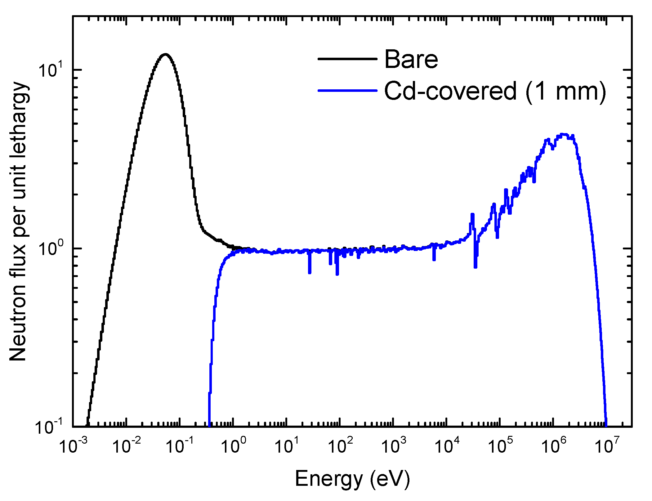
2. Materials and Methods

n-type Schottky barrier diodes (SBDs) were produced on nitrogen-doped (up to 4.5 × 1014 cm−3) 4H-SiC epitaxial layers, approximately 25 µm thick [40]. The epitaxial layer was grown on the silicon face (8° off) of 350 µm thick silicon carbide substrate without the buffer layer. The Schottky barrier was formed by thermal evaporation of nickel through a metal mask with patterned square apertures of 1 mm × 1 mm, while Ohmic contacts were formed on the backside of the silicon carbide substrate by nickel sintering at 950 °C in the Ar atmosphere.
The SBDs were pattern-implanted with 7.5 MeV C and 2 MeV He ions with fluences of 108–109 cm−2 and 109–1010 cm−2, respectively. All implantations were performed through the front nickel Schottky contact, at room temperature and zero applied bias. The selected ion energies provide similar ion depth ranges, which are accessible by the DLTS technique. The pattern-implantation of ions was performed at the ANSTO (Australian Nuclear Science and Technology Organisation) nuclear microprobe facility [41] as described in the previous study [30]. An area of a Schottky contact (1 mm × 1 mm) was divided into 512 pixels × 512 pixels. An ion microbeam raster-scanned multiple times over the contact area, implanting one or two ions at each pixel location before moving to the next location. The specified fluences were calculated as the number of implanted ions per area of Schottky contact. The fluences were specified for each SBD used in this study. The primary displacements created in collision cascades were spatially well separated, and their interaction with defects created in subsequent cascades was negligible. The trajectory of incident ions was normal to the surface of the Schottky contact, not aligned with the crystal axis. Ion depth ranges and total vacancy concentration profiles were calculated using the SRIM (The Stopping and Range of Ions in Matter) code [42].
The SBDs were irradiated with epithermal and fast neutrons at the Jozef Stefan Institute (JSI) TRIGA reactor in Ljubljana, Slovenia. Thermal neutrons with energy less than 0.55 eV were filtered by irradiating the Schottky barrier diodes inside a cadmium box with a wall thickness of 1 mm. The neutron energy spectrum and irradiation settings are the same as in the previously reported study [43]. Figure 1 displays the neutron spectra in the pneumatic tube (PT) irradiation channel, located in the F-24 core position, obtained by Monte Carlo simulation using the MCNP code [44] and subsequently characterized on the basis of experimental neutron activation measurements [45]. Elastic collisions of incident neutrons with atoms of SiC crystal result in the introduction of intrinsic defects. The selected neutron fluences were 1012 cm−2 and 1013 cm−2.
The averaged primary displacement (vacancy) generation rate (VGR) distributions, created in collision cascades of the 2.0 MeV He and 7.5 MeV C ions being implanted in the 4H-SiC epitaxial layer at normal incident not aligned with the crystal axis, was simulated for a total of 10,000 ions using the SRIM code [42]. As shown in Figure 2, the VGR distribution gradually increased from the surface of the epitaxial layer underneath the Ni contact layer and reached a sharp maximum in the 4–5 μm depth range, close to the end of an ion range. The average VGR value per 2.0 MeV He ion was 2.5 × 10⁻³ Å−1. The maximum VGR value for C vacancy was 1.6 × 10⁻² Å−1 and for Si vacancy was 1.2 × 10⁻² Å−1 at a depth equal to 4.7 μm. The difference in silicon and carbon vacancy density is a result of the differences in the displacement threshold values for Si (35 eV) and C atoms (22 eV) in 4H-SiC material [46]. The average VGR value for a single 7.5 MeV C ion was 1.4 × 10⁻² Å−1, while the maximum VGR value for C vacancy was 8.7 × 10⁻² Å−1 and for Si vacancy was 6.4 × 10⁻² Å−1 at a depth equal to 4.6 μm. Therefore, each 7.5 MeV carbon ion produced approximately five and half times more silicon or carbon vacancies than each 2.0 MeV helium ion (alpha particle) used in this study.
The displacement damage introduced by neutron irradiation in the 4H-SiC epitaxial layer was simulated by Fluka software [47]. The neutron spectrum shown in Figure 1 (blue line) was used to select the neutron energies used in the simulation (627 values in the range 2 × 10⁻⁴–2 × 10⁷ eV) and to calculate the average displacement generation rate. A total of 106 incident neutrons were simulated for each energy. The calculated displacement profile was used as the estimate of the vacancy concentration profile.
The temperature-dependent current–voltage (I–V) and capacitance–voltage (C–V) characteristics of SBDs were measured using a Keithley 4200 SCS (Keithley Instruments, Cleveland, OH, USA). Radiation induced electrically active defects were characterized by the DLTS technique. DLTS measurements were carried out in the temperature range from 100 to 380 K. The SBDs were cooled down from room temperature without an applied bias before DLTS measurements. Subsequently, low temperature annealing at a temperature of 450 K for 30 min and a series of DLTS measurements in the temperature range up to 450 K were carried out. Before DLTS measurements, the SBDs were cooled down from 340 K with applied bias (−30 V) or 450 K without applied bias to observe A and B configurations of the M-center, respectively. The temperature ramp rate was 2 K/min. Concentration profiles of deep level defects were determined from their DLTS amplitude, where different depth ranges were probed by increasing reverse bias VR in a step of 0.5 V and keeping constant the difference between pulse bias and reverse bias VP − VR = 1 V. The lambda effect [48,49] was taken into account. Capacitance transients were measured using a Boonton 7200 capacitance meter and the following acquisition settings: number of samples 3 × 10⁴, sampling rate 10–80 kHz, and number of averaged scans 100–800. The FLOG numerical routine [50] was used for the calculation of Laplace DLTS spectra.

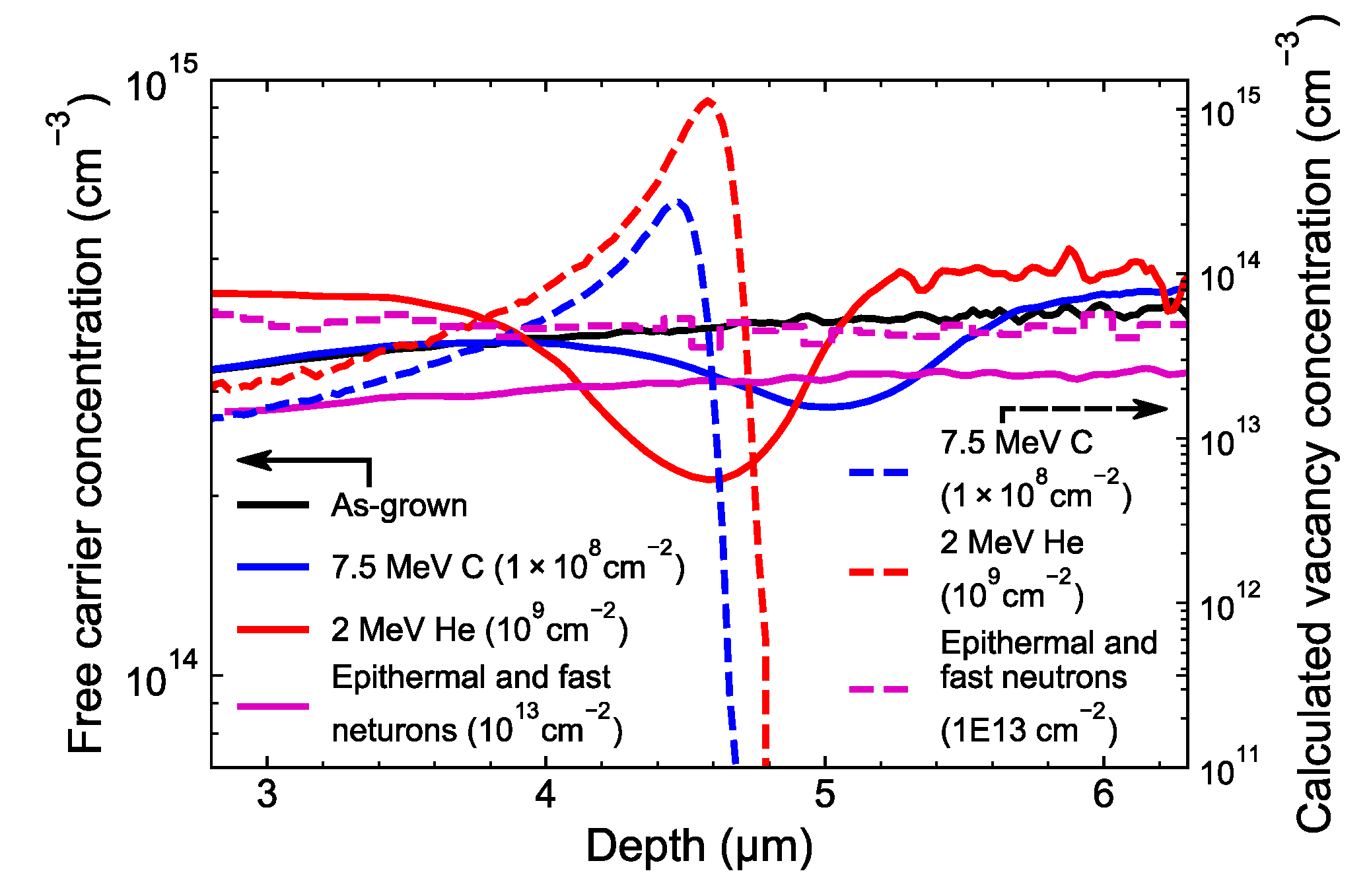
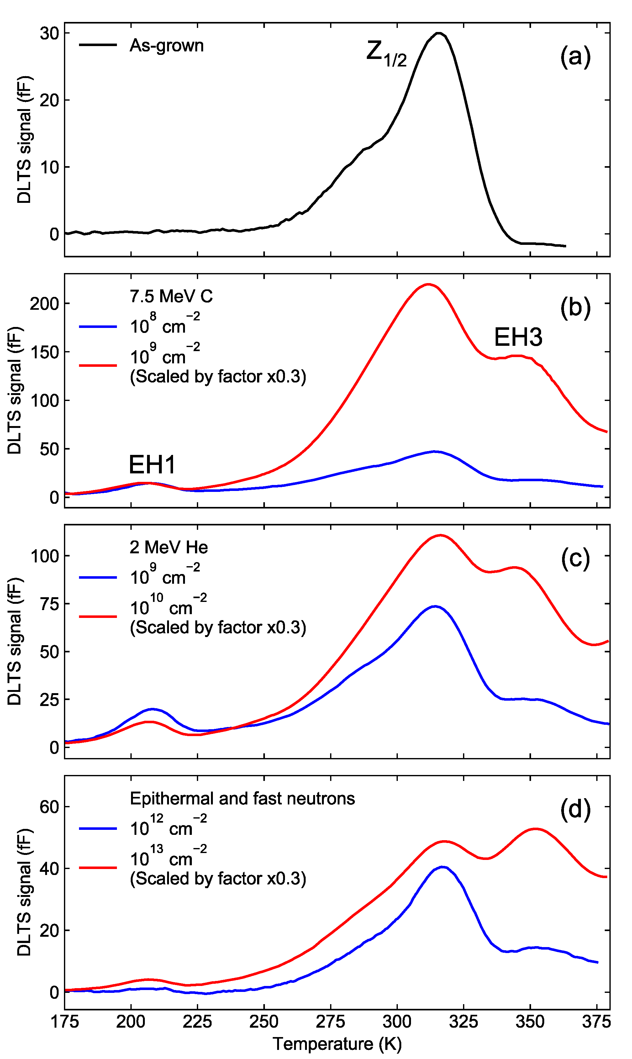
3. Results and Discussion

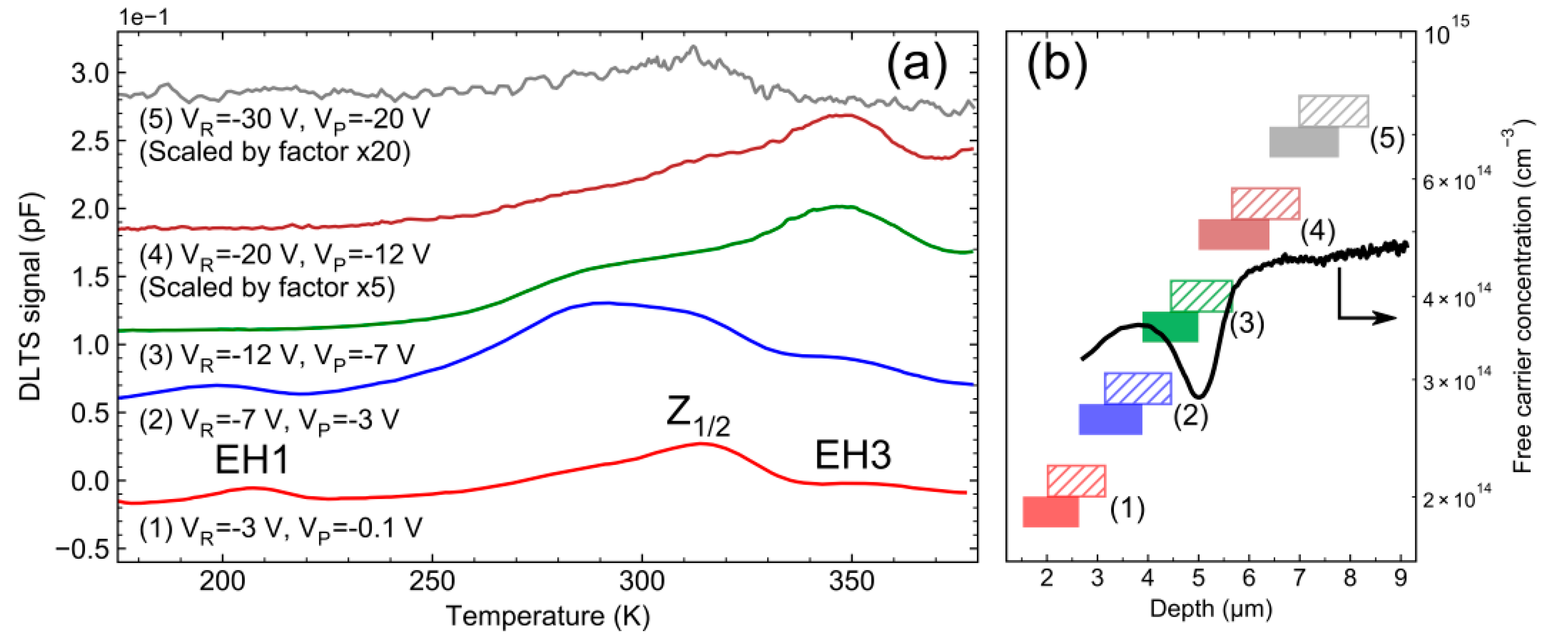
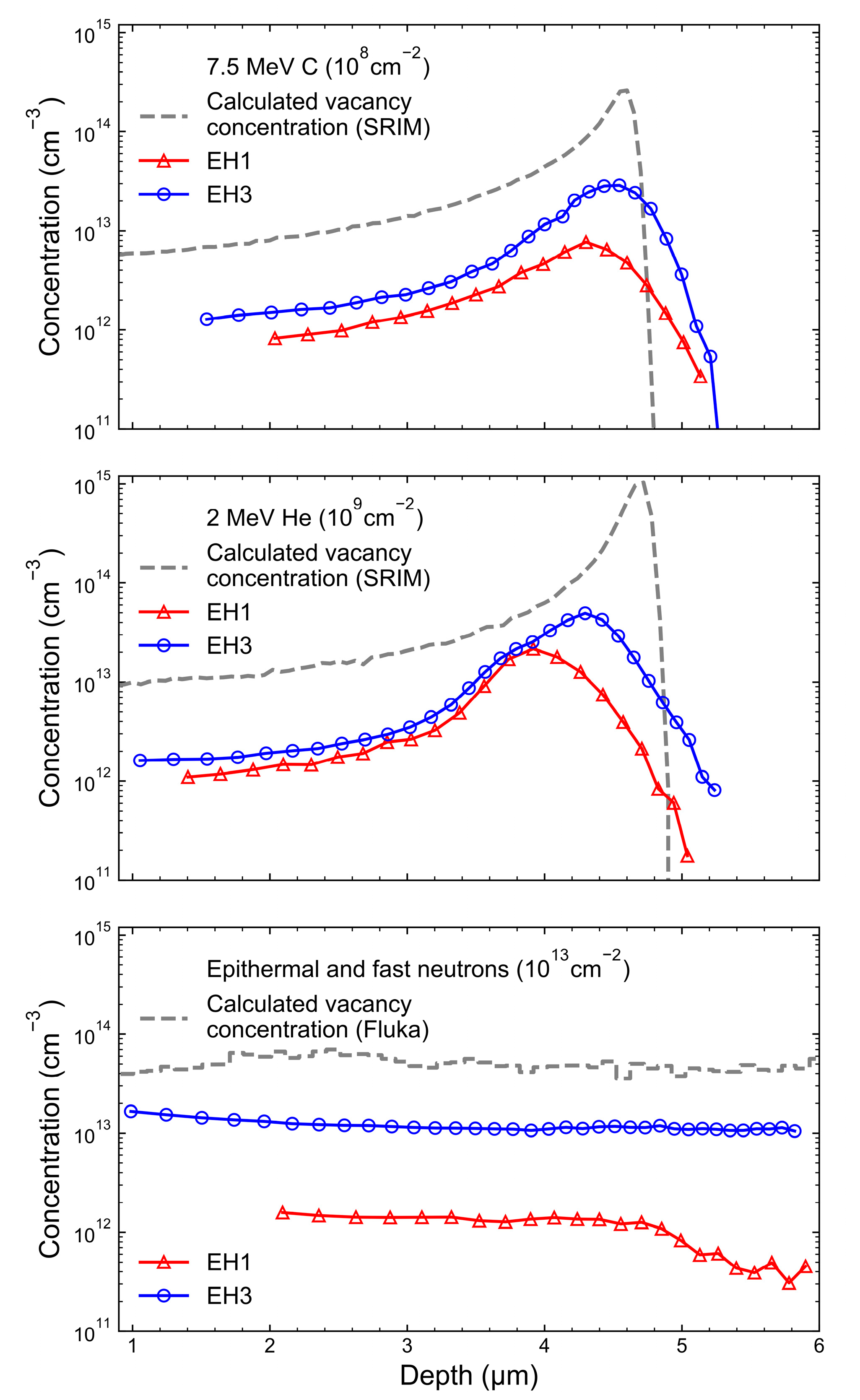
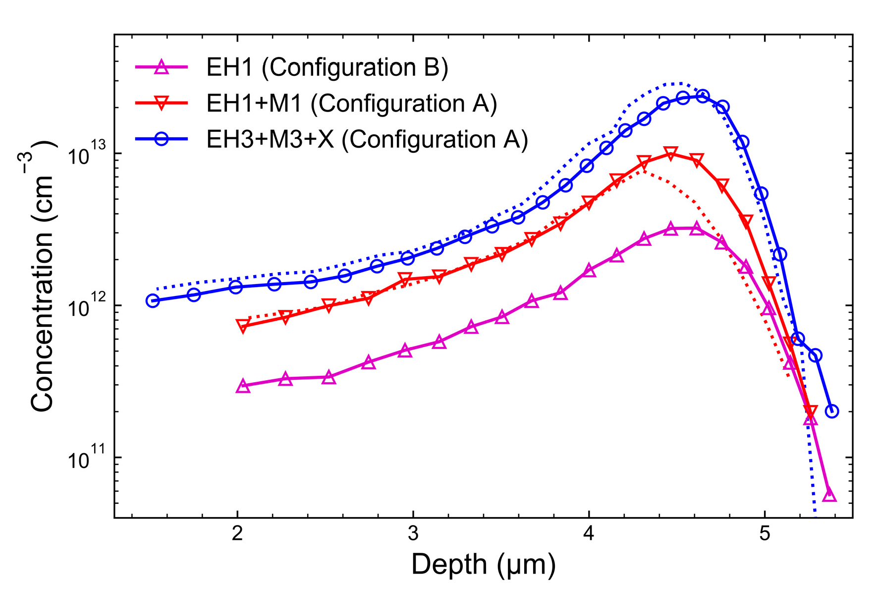
3.1. Depth Profiling of EH1 and EH3 Deep Level Defects

The quality of the prepared SBDs was checked by temperature dependent current–voltage (I–V–T) and capacitance–voltage (C–V–T) measurements and they showed excellent rectifying characteristics (see Figure S1).
Figure 2 shows the effect of ion implantation and neutron irradiation on the free carrier concentration profile of 4H-SiC SBDs. Introduced defects caused a reduction of free carrier concentration as the free carriers were captured by the introduced acceptor deep levels. In as-grown and neutron irradiated SBDs, a homogenous free carrier concentration was observed. The free carrier concentration in 7.5 MeV C ion implanted SBDs had a minimum at a depth of 4.8–5.0 μm close to the calculated ion depth range at 4.55 μm. Likewise, in 2 MeV He ion implanted SBDs the minimum of the free carrier concentration and ion depth range were at 4.5–4.9 μm and 4.67 μm, respectively.
DLTS spectra of as-grown, ion implanted, and neutron irradiated 4H-SiC SBDs are shown in Figure 3. Only one asymmetric peak, labeled as Z1/2, was present in the DLTS spectrum for as-grown 4H-SiC. The Z1/2 is a well-known deep level and previously assigned to a transition between double negative and neutral charge state of carbon vacancy VC (=/0) [52]. As recently reported [23,24], two emission lines Z1 (=/0) and Z2 (=/0) are resolved by the Laplace DLTS technique and assigned to carbon vacancies residing on two different lattice sites with local cubic and hexagonal symmetry.
The concentration of Z1/2 and introduced two additional deep levels, labeled as EH1 and EH3, was increased by ion implantation and neutron irradiation. Activation energies and apparent electron captured cross-sections of observed deep levels are listed in Table 1. A fact that the same types of deep levels were produced by implantation of two different types of ions (light and medium heavy) and neutrons clearly indicate that they were intrinsic defects [53]. The energy of impinging ions and neutrons was high enough to displace silicon atoms in the 4H-SiC crystal lattice. The observed EH1 and EH3 deep levels were recently assigned to VSi (−3/=) and VSi (=/−) transitions of silicon vacancy VSi [32], respectively. Two emission lines for the EH1 deep level defect were recently resolved by the Laplace DLTS technique [31,32], and assigned to VSi residing on two different sites in the crystal with local cubic and hexagonal symmetry (Figure 4).
Figure 5a shows the DLTS spectra of 7.5 MeV C implanted (108 cm−2) SBD with different bias settings for probing deep levels in the adjacent depth ranges. The EH1 and EH3 defects located in the depth regions illustrated by hatched and solid rectangles in Figure 5b contribute to their DLTS signals at 210 K and 350 K shown in Figure 5a. Defects in different probed depth regions were mutually compared in regard with the measured free carrier concentration (black line), which exhibited a minimum due to carrier capture in the introduced acceptor levels. We assumed that the concentration of the introduced acceptor levels is the largest approximately at the position of the minimum in free carrier concentration. The amplitudes of peaks assigned to EH1 and EH3 defects are roughly the same in the DLTS spectrum obtained probing the depth region closest to the surface (red and blue curves), which is in agreement with reports of other authors [27,32]. The peak assigned to the EH3 defect shows a rapid increase, while the peak assigned to the EH1 defect disappeared in the region coinciding with the minimum in free carrier concentration (green curve in Figure 5a). The peak assigned to the EH3 defect had the largest amplitude in the DLTS spectrum, which was showing deep levels in the depth range beyond the minimum of free carrier concentration, while the peak assigned to the EH1 defect was not observed in that region (brown curve in Figure 5a). DLTS spectrum probing the depth region farthest from the ion implanted region (gray curve) contained only one small peak, the Z1/2 defect, which was present in as-grown 4H-SiC. DLTS measurements on 2 MeV He implanted (109 cm−2) SBD show that concentrations of EH1, Z1/2, and EH3 deep levels varied with depth in the same way as in the case of 7.5 MeV C implanted (108 cm−2) SBD (see Figure S2).
The measured concentration profiles for EH1 and EH3 deep levels are shown in Figure 6. Lambda-corrected depth concentration profiles were estimated from DLTS signal amplitude Δ C using the following equation [49]:
N T ( x )   = 2 N S C R ( W R ) ( 1 λ R W R ) 2 ( W P λ P W R ) 2 Δ C C R
where C R , W R ( W P ), and λ R ( λ P ) are steady state capacitance, space charge region width, and lambda length at reverse bias VR (pulse bias VP), respectively. Voltage settings were selected to probe deep levels in narrow depth range, whose midpoint is at x = [ ( W R λ R ) + ( W P λ P ) ] / 2 . The charge concentration N S C R ( W R ) at the edge of the space charge depletion region [48], W R , and W P were determined from the C–V characteristics at the measurement temperature. The lambda lengths were calculated using the free carrier concentration profile measured at the temperature of 200 K (as seen in Figure 2), which corresponds to the net donor concentration [51], and known activation energy (Table 1).
The estimated ratio of EH1 and EH3 deep level concentrations in ion implanted SBDs was close to 1:2 at the depths below the ion depth range (2–3 μm), while around the ion depth range the [EH1]:[EH3] ratio varied. The maximum of EH3 concentration profile was about four times larger than the maximum of EH1 concentration in C (108 cm−2) implanted SBD, while it was two times larger in He (109 cm−2) ion implanted SBD. At the depths below the ion depth range, the shape of EH1 and EH3 concentration profiles followed the shape of the calculated concentration profile of the total introduced vacancies.
As previously mentioned, EH1 and EH3 deep levels with activation energies around 0.4 eV and 0.7 eV were assigned to VSi (−3/=) and VSi (=/−) transitions of the silicon vacancy. In those transitions, the emission of a single electron from the same defect occurred. Therefore, we should observe the same concentration of deep levels assigned to VSi. In previous studies [32,54], the one-to-one correlation between their concentrations enabled their assignment to the transitions of the same defect. An increased concentration of the EH3 deep level compared to EH1 in a region beyond the maximum of SRIM calculated that the distribution of atomic displacements could be explained by the contribution of deep levels other than VSi (=/−) with similar activation energy to the total measured DLTS signal. A slight shift of the maximum of EH3 deep level profile towards larger depths compared to the EH1 deep level profile could indicate that the EH3 deep level defect, which is not necessary VSi, contains interstitials. In their study, Pellegrino et al. [55] demonstrated that a forward momentum transfer from the impinging ions to the lattice atoms in silicon can result in displacement between maximal values of vacancy and self-interstitial depth distributions. The EH1 deep level concentration had a maximum at a depth of 4.3 ± 0.2 μm in C (108 cm−2) ion implanted SBD, while the EH3 deep level concentration had a maximum at 4.5 ± 0.1 μm. Likewise, concentrations of EH1 and EH3 deep levels in He (109 cm−2) ion implanted SBD had maximums at depths of 3.9 ± 0.2 μm and 4.3 ± 0.1 μm, respectively. The concentration of the Z1/2 deep level was the largest at a depth of 4.4 ± 0.1 μm in the C (108 cm−2) ion implanted SBD and at a depth of 3.8 ± 0.1 μm in the He (109 cm−2) ion implanted SBD, which was close to the maximum of EH1 defect concentration profile. The Z1/2 defect distribution depth profile agrees with previous studies [15].
In the case of neutron irradiation, a higher concentration of the EH1 deep level was observed at depths below 5 μm. The region with higher EH1 concentration was inside the space charge region at reverse voltage −10 V used during DLTS measurements in the temperature range up to 380 K. As previously reported [27,56], EH1 and EH3 deep levels can be observed after a sufficiently long time annealing in the temperature range 350–400 K without bias, while the applied bias enhances process related to their appearance. Therefore, EH1 concentration outside the space charge region was lower as the process related to its appearance was incomplete during low temperature annealing in the temperature range 350–380 K. The concentration of the peak at 350 K resulting from multiple overlapping deep levels was much higher than EH1 deep level concentration. Thus, a decrease in concentration at greater depths was not pronounced.
Laplace DLTS spectra for EH1 and EH3 deep levels are shown in Figure 7. The observed EH3 peak was broad and in the vicinity of other peaks, like Z2 (=/0), which affected the resolution. Contrary to EH1 peak, which was recently resolved into two emission lines [31], the EH3 peak could not be resolved by the Laplace DLTS technique. Moreover, a presence of an unresolved deep level, which is indicated by the measured concentration profiles (Figure 6), could lead to the broadening of the EH3 peak in the Laplace spectra. The used FLOG numerical routine calculated the Laplace DLTS spectra with the least possible number of peaks, which described well the measured capacitance transient, consistent with the measured data points and signal to noise ratio [50]. It is challenging to resolve a higher number of deep levels with closely spaced emissions. However, the matching of the Laplace DLTS spectra (for EH1 and EH3 deep levels) confirmed the observation of the same type of defects.

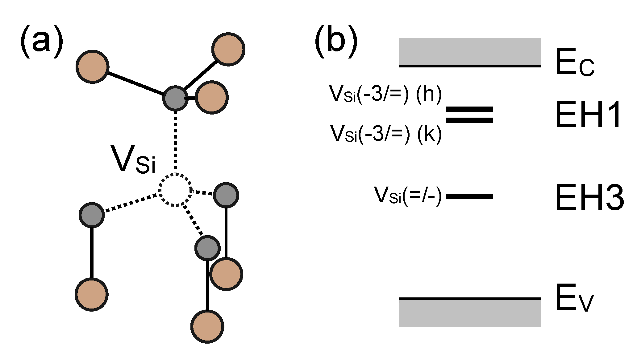
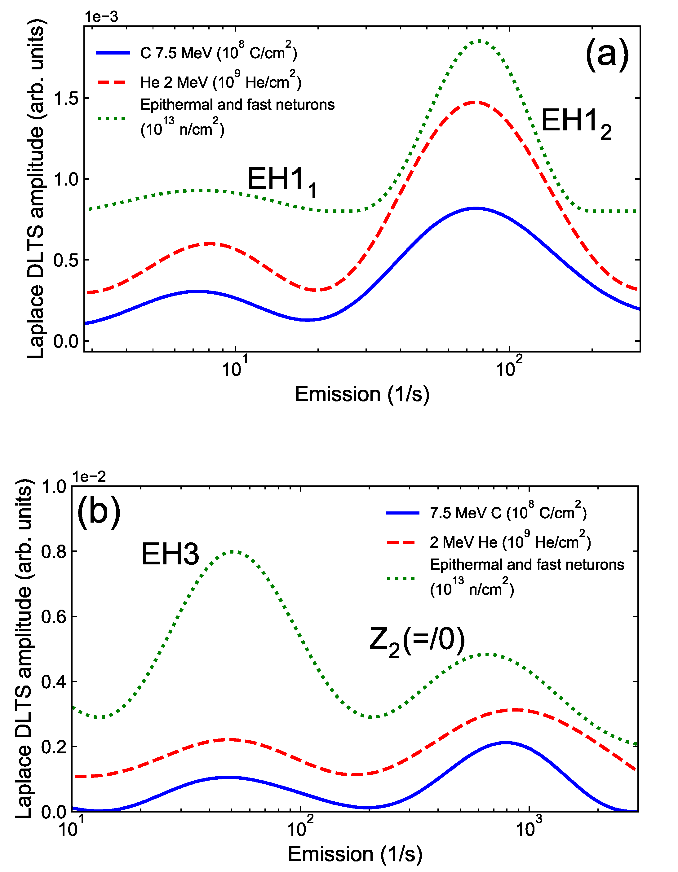
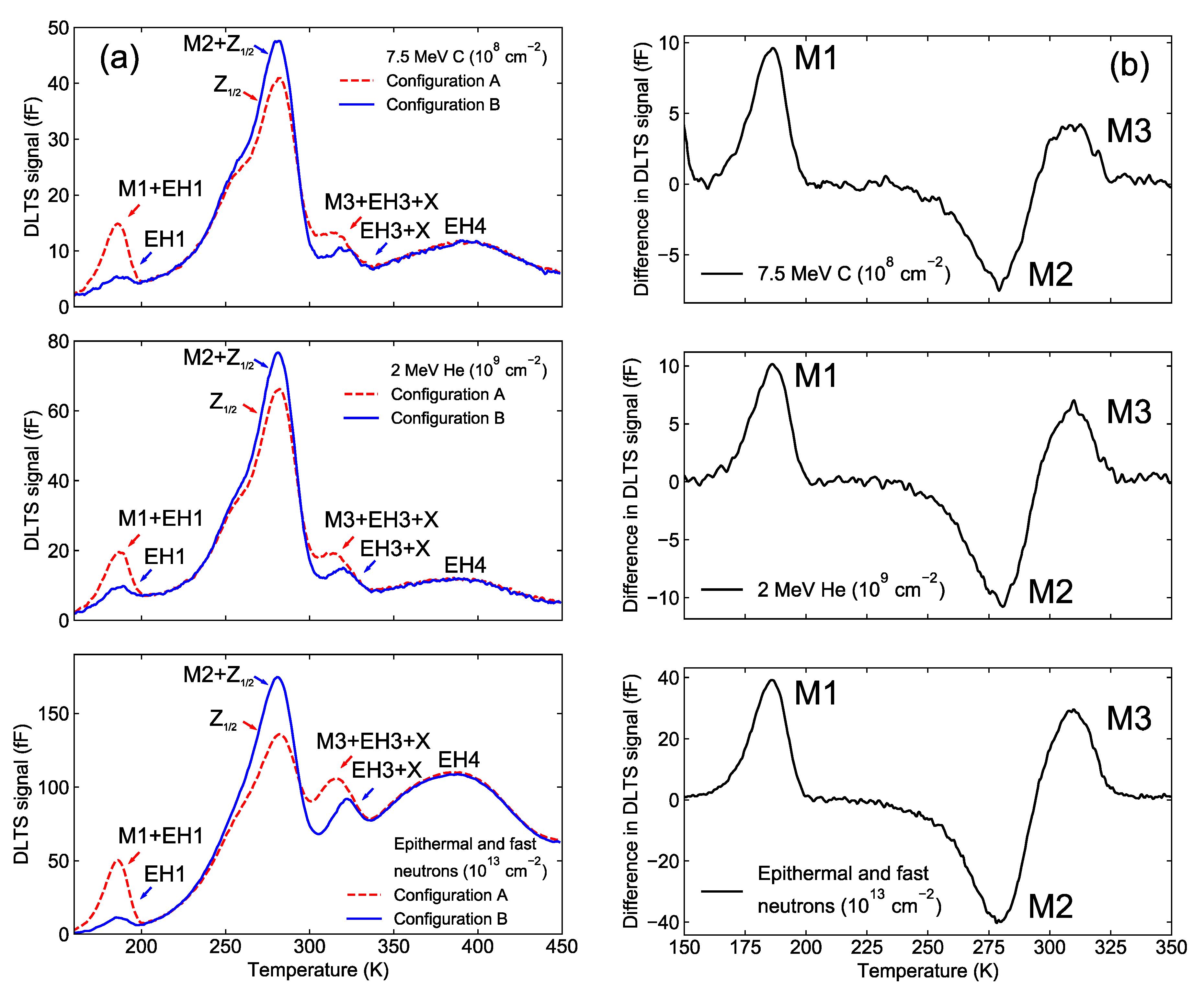
3.2. Metastable Defects

In order to obtain additional information on unresolved deep levels, we applied the low-temperature annealing and DLTS measurements in the temperature range up to 450 K. The influence of low temperature annealing on EH1 and EH3 deep levels has already been reported in several studies [27,30,34,35,36,37,38,56]. Pastuovic et al. [30] have reported on changes of EH1 and EH3 deep level concentrations (labeled ET1 and ET2) after low temperature annealing in the temperature range up to 700 K. EH1 and EH3 deep levels completely anneal out in the temperature range from 600 to 700 K [28,30,37], accompanied by free carrier concentration recovery. DLTS measurements that occur after the initial annealing at 450 K for 30 min and measurement in the temperature range up to 450 K are stable, the unintentional annealing during the measurement does not affect DLTS spectra.
As seen in Figure 8a, the additional deep level labeled as EH4 was observed with an activation energy of 0.83–1.05 eV. The EH4 deep level was previously assigned to a defect complex or cluster of first-order defects [17,28,30]. Recently, a model of the broad EH4 peak was proposed consisting of three deep levels attributed to (+/0) transition of the carbon antisite-carbon vacancy complex in three energetically inequivalent configurations [57]. However, a possibility is left that other deep level defects, such as di-vacancy, also contribute to a broad EH4 peak.
As previously mentioned, the depth profiling measurements (Figure 6) indicate that an interstitially related deep level defect contributes to the DLTS signal at the temperature of the EH3 deep level. In Figure 8a and henceforward, this contribution is separately labeled as X.
Additionally, the metastable M-center was detected in the neutron irradiated and ion implanted 4H-SiC (Figure 8a). In previous studies [34,35,36,37,38], the introduction of the M-center was reported only in the cases of proton and electron irradiation. The M-center was transformed to configuration B by cooling down SBDs from 450 K without applied bias, while configuration A was realized by cooling down SBDs with applied bias (−30 V) from above room temperature (340 K). M1 and M3 deep levels of the M-center were observed in configuration A, while the M2 deep level was observed in configuration B. They were resolved by subtracting two DLTS spectra with the M-center in configuration A and configuration B, as shown in Figure 8b. In a first approximation, the difference in DLTS spectra was only due to M-center deep levels [35]. The approximation was the best in the case of neutron irradiated (1013 cm−2) SBD due to the higher reverse voltage used in the measurements (−10 V) and uniform deep level concentrations. The coordinate configuration diagram describing the observed transitions of the M-center is shown in Figure 9. The shown transitions are consistent with previously reported findings [36]. Activation energies of M1 and M2 deep levels were determined using the subtracted DLTS spectra, while activation energy of the M3 deep level was estimated based on the activation energy of the EH3 + M3 + X peak. The subtracted DLTS spectra provided too few points for the Arrhenius graph of the M3 deep level due to the transition of the M-center to A configuration during DLTS measurements at temperatures above 300 K. As best seen in the case of neutron irradiation due to uniform concentration of deep levels, the concentrations of M1 and M2 deep levels were the same. A smaller peak height (concentration) of the M3 deep level seen in Figure 8b was due to the previously mentioned partial transformation of the M-center to A configuration during DLTS measurement.
The concentration profiles measured on the C (108 cm−2) ion implanted SBD after 450 K annealing are shown in Figure 10. The concentration profile of EH1 was measured with the M center in configuration B, while EH1 + M1 and EH3 + M3 + X concentration profiles were measured with the M-center in configuration A. The overlap of profiles measured at a temperature of 210 K before (dotted lines) and after 450 K annealing indicates that the M-center was present in ion implanted SBDs before 450 K annealing at depths below the ion depth range. Moreover, an increase in M-center concentration at an ion depth range and a slight decrease in the EH3 + M3 + X concentration in the region below the ion depth range was observed after 450 K annealing. A decrease in the EH3 + M3 + X concentration profile could be due to defect reactions involving carbon interstitials, which are mobile at temperatures above 450 K [58]. The concentration profile of the M-center did not show significant deviation from EH1 concentration profile. In neutron irradiated SBD, uniform concentrations of the M-center, EH1, and EH3 deep levels were observed in the whole depth range (see Figure S5).
M1 and M3 deep levels were not resolved by Laplace DLTS measurements. The EH12 and EH3 peaks seen in Figure 7 partially contained the contributions of M1 and M3 deep levels, respectively.
In this work, we utilized a depth and energy resolution of DLTS measurements to obtain concentration profiles of deep levels introduced by ion implantation and irradiation, and compared them relative to the vacancy profile. The transformation of the M-center between A and B configurations was used to resolve M1, M2, and M3 deep levels in the DLTS spectra and obtain information on the M-center depth profile. The identification of the M-center is still uncertain with previously reported studies.

4. Conclusions

We reported on a comparative DLTS study of EH1 and EH3 deep level defects in 4H-SiC introduced by C and He ion implantation and neutron irradiation. Their intrinsic origin was confirmed. We analyzed components of EH1 and EH3 deep levels by depth profiling and annealing procedure. Our results show that the deep levels of silicon vacancy, the M-center, and the defect involving interstitials contributed simultaneously to the DLTS signal at the temperature of EH1 and EH3 deep levels. The shift of the EH3 concentration profile maximum towards greater depths and higher concentration relative to EH1 concentration profile was observed and explained by the presence of an additional defect involving interstitials. Introduction of the M-center by different types of ion implantation and irradiation was demonstrated, leading to a hypothesis that the M-center was also an intrinsic defect.

Supplementary Materials

The following are available online at https://0-www-mdpi-com.brum.beds.ac.uk/2073-4352/10/9/845/s1, Figure S1: Current-voltage characteristics of SBDs implanted with 7.5 MeV C (108 cm−2) and 2 MeV He (109 cm−2) ions, and neutron irradiated (1013 cm−2) SBD at temperatures of 200 K and 300 K, Figure S2: (a) DLTS spectra of 2 MeV He (109 cm−2) ion implanted n-type 4H-SiC SBD. Different voltage settings, reverse bias VR and pulse bias VP, are used to probe different depth ranges (as seen in (b)). The rate window and pulse width tP are 50 s−1 and 10 ms. The spectra are shifted vertically for clarity. (b) Schematic illustration of the depth regions contributing to the DLTS signal of EH1 at 210 K (hatched rectangles) and EH3 at 350 K (solid rectangles) for the used voltage in the DLTS measurements (as seen in (a)). The lambda effect was taken into account. The depth ranges are compared with free carrier concentration (black line) determined from C–V characteristic at 200 K (as in Figure 2), which exhibits a minimum due to introduced acceptor deep levels, Figure S3: Depth concentration profiles for Z1/2 deep level and total introduced vacancies calculated by SRIM and Fluka software [1,2]. The lambda effect was taken into account [3]. Depth profiling measurements were carried out at the temperature of 315 K, Figure S4: Increase in free carrier concentration after annealing at the temperature of 450 K. Solid and dashed lines show free carrier concentration profiles measured before and after annealing at the temperature of 450 K, respectively. The profiles are calculated using C–V measurements at a temperature of 200 K, Figure S5: EH1, EH1 and M1, EH3 and M3 depth concentration profiles in (a) 2 MeV He (109 cm−2) ion implanted and (b) neutron (1013 cm−2) irradiated SBD. The shown EH1 + M1 concentration profile (Configuration A) was measured after cooling SBD from 340 K down to 210 K under −30V bias, while EH1 profile was measured after cooling down SBD from 450 K without bias. The black curve in (b) shows depth concentration profile measured after cooling SBD from 340 K down to 210 K under −10V bias. Depth profiles measured before 450 K annealing (as seen in Figure 6) are shown with dotted lines. The contribution of an additional deep level defect involving interstitials is labeled as X, Figure S6: Pulse width dependence of EH1 and EH1 + M1 DLTS signal amplitudes in neutron (1013 cm−2) irradiated SBD. DLTS signal amplitude of M1 deep level is determined by subtracting EH1 + M1 and EH1 DLTS signals. Measurements are carried out at a temperature of 210 K using 50 1/s emission rate window. Reverse and pulse voltages were −10 V and −0.1 V, respectively.

Author Contributions

Formal analysis, T.B., Ž.P.; investigation, T.B., L.B., I.C., L.S., V.R., Ž.P.; resources, T.O.; writing—original draft preparation, T.B., I.C.; writing—review and editing, T.B., I.C., L.S., V.R., Ž.P.; supervision, I.C. All authors have read and agreed to the published version of the manuscript.

Funding

This research was funded by NATO SPS Program, grant number 985215. The authors acknowledge the financial support from the Slovenian Research Agency (research core funding No. P2-0073). This research was partially funded by the National Collaborative Research Infrastructure Strategy (NCRIS) funding provided by the Australian Government.

Acknowledgments

We would like to acknowledge Hidekazu Tsuchida and Norihiro Hoshino of Central Research Institute of Electric Power Industry for the supply of SiC substrates with epitaxially grown 4H–SiC single-crystal layers. The authors acknowledge assistance by the TRIGA research reactor operators.

Conflicts of Interest

The authors declare no conflict of interest.

References

  1. Hedayati, R.; Lanni, L.; Rodriguez, S.; Malm, B.G.; Rusu, A.; Zetterling, C.M. A monolithic, 500 °C operational amplifier in 4H-SiC bipolar technology. IEEE Electron. Device Lett. 2014, 35, 693–695. [Google Scholar] [CrossRef] [Green Version]
  2. Ryu, S.-H.; Krishnaswami, S.; Hull, B.; Heath, B.; Das, M.; Richmond, J.; Fatima, H.; Zhang, J.; Agarwal, A.; Palmour, J.; et al. High Speed Switching Devices in 4H-SiC—Performance and Reliability. In Proceedings of the 2005 IEEE International Semiconductor Device Research Symposium, Bethesda, MD, USA, 7–9 December 2005; pp. 162–163. [Google Scholar]
  3. Wang, J.; Zhou, Y.; Zhang, X.; Liu, F.; Li, Y.; Li, K.; Liu, Z.; Wang, G.; Gao, W. Efficient Generation of an Array of Single Silicon-Vacancy Defects in Silicon Carbide. Phys. Rev. Appl. 2017, 7, 064021. [Google Scholar] [CrossRef]
  4. Widmann, M.; Lee, S.Y.; Rendler, T.; Son, N.T.; Fedder, H.; Paik, S.; Yang, L.P.; Zhao, N.; Yang, S.; Booker, I.; et al. Coherent control of single spins in silicon carbide at room temperature. Nat. Mater. 2015, 14, 164–168. [Google Scholar] [CrossRef] [PubMed] [Green Version]
  5. Fuchs, F.; Stender, B.; Trupke, M.; Simin, D.; Pflaum, J.; Dyakonov, V.; Astakhov, G.V. Engineering near-infrared single-photon emitters with optically active spins in ultrapure silicon carbide. Nat. Commun. 2015, 6, 1–7. [Google Scholar] [CrossRef] [Green Version]
  6. Wolfowicz, G.; Anderson, C.P.; Yeats, A.L.; Whiteley, S.J.; Niklas, J.; Poluektov, O.G.; Heremans, F.J.; Awschalom, D.D. Optical charge state control of spin defects in 4H-SiC. Nat. Commun. 2017, 8, 2–10. [Google Scholar] [CrossRef]
  7. Kasper, C.; Klenkert, D.; Shang, Z.; Simin, D.; Gottscholl, A.; Sperlich, A.; Kraus, H.; Schneider, C.; Zhou, S.; Trupke, M.; et al. Influence of Irradiation on Defect Spin Coherence in Silicon Carbide. Phys. Rev. Appl. 2020, 13, 044054. [Google Scholar] [CrossRef] [Green Version]
  8. Szász, K.; Ivády, V.; Abrikosov, I.A.; Janzén, E.; Bockstedte, M.; Gali, A. Spin and photophysics of carbon-antisite vacancy defect in 4H silicon carbide: A potential quantum bit. Phys. Rev. B Condens. Matter Mater. Phys. 2015, 91, 1–5. [Google Scholar] [CrossRef] [Green Version]
  9. Hazdra, P.; Vobecký, J. Accurate simulation of fast ion irradiated power devices. Solid State Electron. 1994, 37, 127–134. [Google Scholar] [CrossRef]
  10. Yang, A.; Murata, K.; Miyazawa, T.; Tawara, T.; Tsuchida, H. Analysis of carrier lifetimes in N + B-doped n -type 4H-SiC epilayers. J. Appl. Phys. 2019, 126, 055103. [Google Scholar] [CrossRef]
  11. Radulović, V.; AmbroZič, K.; Snoj, L.; Capan, I.; Brodar, T.; Ereš, Z.; Pastuović, Z.; Sarbutt, A.; Ohshima, T.; Yamazaki, Y.; et al. E-SiCure Collaboration Project: Silicon Carbide Material Studies and Detector Prototype Testing at the JSI TRIGA Reactor. EPJ Web Conf. 2020, 225, 07007. [Google Scholar] [CrossRef] [Green Version]
  12. Puglisi, D.; Bertuccio, G. Silicon Carbide Microstrip Radiation Detectors. Micromachines 2019, 10, 835. [Google Scholar] [CrossRef] [PubMed] [Green Version]
  13. Mandal, K.C.; Kleppinger, J.W.; Chaudhuri, S.K. Advances in High-Resolution Radiation Detection Using 4H-SiC Epitaxial Layer Devices. Micromachines 2020, 11, 254. [Google Scholar] [CrossRef] [PubMed] [Green Version]
  14. Kimoto, T.; Danno, K.; Suda, J. Lifetime-killing defects in 4H-SiC epilayers and lifetime control by low-energy electron irradiation. Phys. Status Solidi 2008, 245, 1327–1336. [Google Scholar] [CrossRef]
  15. Hazdra, P.; Popelka, S.; Schöner, A. Local Lifetime Control in 4H-SiC by Proton Irradiation. Mater. Sci. Forum 2018, 924, 436–439. [Google Scholar] [CrossRef]
  16. Galeckas, A.; Ayedh, H.M.; Bergman, J.P.; Svensson, B.G. Depth-Resolved Carrier Lifetime Measurements in 4H-SiC Epilayers Monitoring Carbon Vacancy Elimination. Mater. Sci. Forum 2017, 897, 258–261. [Google Scholar] [CrossRef]
  17. Storasta, L.; Bergman, J.P.; Janzén, E.; Henry, A.; Lu, J. Deep levels created by low energy electron irradiation in 4H-SiC. J. Appl. Phys. 2004, 96, 4909–4915. [Google Scholar] [CrossRef]
  18. Saito, E.; Suda, J.; Kimoto, T. Control of carrier lifetime of thick n-type 4H-SiC epilayers by high-temperature Ar annealing. Appl. Phys. Express 2016, 9, 061303. [Google Scholar] [CrossRef]
  19. Miyazawa, T.; Tsuchida, H. Point defect reduction and carrier lifetime improvement of Si- and C-face 4H-SiC epilayers. J. Appl. Phys. 2013, 113, 083714. [Google Scholar] [CrossRef]
  20. Storasta, L.; Tsuchida, H. Reduction of Traps and Improvement of Carrier Lifetime in SiC Epilayer by Ion Implantation. Mater. Sci. Forum 2007, 556–557, 603–606. [Google Scholar] [CrossRef]
  21. Kushibe, M.; Nishio, J.; Iijima, R.; Miyasaka, A.; Asamizu, H.; Kitai, H.; Kosugi, R.; Harada, S.; Kojima, K. Carrier Lifetimes in 4H-SiC Epitaxial Layers on the C-Face Enhanced by Carbon Implantation. Mater. Sci. Forum 2018, 924, 432–435. [Google Scholar] [CrossRef]
  22. Kawahara, K.; Thang Trinh, X.; Tien Son, N.; Janzén, E.; Suda, J.; Kimoto, T. Quantitative comparison between Z 1/2 center and carbon vacancy in 4H-SiC. J. Appl. Phys. 2014, 115, 143705. [Google Scholar] [CrossRef] [Green Version]
  23. Capan, I.; Brodar, T.; Coutinho, J.; Ohshima, T.; Markevich, V.P.; Peaker, A.R. Acceptor levels of the carbon vacancy in 4 H -SiC: Combining Laplace deep level transient spectroscopy with density functional modeling. J. Appl. Phys. 2018, 124, 245701. [Google Scholar] [CrossRef] [Green Version]
  24. Capan, I.; Brodar, T.; Pastuović, Z.; Siegele, R.; Ohshima, T.; Sato, S.I.; Makino, T.; Snoj, L.; Radulović, V.; Coutinho, J.; et al. Double negatively charged carbon vacancy at the h- and k-sites in 4H-SiC: Combined Laplace-DLTS and DFT study. J. Appl. Phys. 2018, 123, 161597. [Google Scholar] [CrossRef] [Green Version]
  25. Paradzah, A.T.; Auret, F.D.; Legodi, M.J.; Omotoso, E.; Diale, M. Electrical characterization of 5.4 MeV alpha-particle irradiated 4H-SiC with low doping density. Nucl. Instrum. Methods Phys. Res. Sect. B Beam Interact. Mater. Atoms. 2015, 358, 112–116. [Google Scholar] [CrossRef] [Green Version]
  26. Omotoso, E.; Meyer, W.E.; Auret, F.D.; Paradzah, A.T.; Legodi, M.J. Electrical characterization of deep levels created by bombarding nitrogen-doped 4H-SiC with alpha-particle irradiation. Nucl. Instrum. Methods Phys. Res. Sect. B Beam Interact. Mater. Atoms. 2016, 371, 312–316. [Google Scholar] [CrossRef] [Green Version]
  27. David, M.L.; Alfieri, G.; Monakhov, E.M.; Hallén, A.; Blanchard, C.; Svensson, B.G.; Barbot, J.F. Electrically active defects in irradiated 4H-SiC. J. Appl. Phys. 2004, 95, 4728–4733. [Google Scholar] [CrossRef]
  28. Alfieri, G.; Monakhov, E.V.; Svensson, B.G.; Linnarsson, M.K. Annealing behavior between room temperature and 2000 °C of deep level defects in electron-irradiated n-type 4H silicon carbide. J. Appl. Phys. 2005, 98, 043518. [Google Scholar] [CrossRef]
  29. Iwamoto, N.; Johnson, B.C.; Hoshino, N.; Ito, M.; Tsuchida, H.; Kojima, K.; Ohshima, T. Defect-induced performance degradation of 4H-SiC Schottky barrier diode particle detectors. J. Appl. Phys. 2013, 113, 143714. [Google Scholar] [CrossRef]
  30. Pastuović, Z.; Siegele, R.; Capan, I.; Brodar, I.; Sato, S.; Ohshima, T. Deep level defects in 4H-SiC introduced by ion implantation: The role of single ion regime. J. Phys. Condens. Matter 2017, 29, 475701. [Google Scholar] [CrossRef]
  31. Capan, I.; Brodar, T.; Yamazaki, Y.; Oki, Y.; Ohshima, T.; Chiba, Y.; Hijikata, Y.; Snoj, L.; Radulović, V. Influence of neutron radiation on majority and minority carrier traps in n-type 4H-SiC. Nucl. Instrum. Methods Phys. Res. Sect. B Beam Interact. Mater. Atoms. 2020, 478, 224–228. [Google Scholar] [CrossRef]
  32. Bathen, M.E.; Galeckas, A.; Müting, J.; Ayedh, H.M.; Grossner, U.; Coutinho, J.; Frodason, Y.K.; Vines, L. Electrical charge state identification and control for the silicon vacancy in 4H-SiC. NPJ Quantum Inf. 2019, 5, 111. [Google Scholar] [CrossRef] [Green Version]
  33. Hornos, T.; Gali, A.; Svensson, B.G. Large-Scale Electronic Structure Calculations of Vacancies in 4H-SiC Using the Heyd-Scuseria-Ernzerhof Screened Hybrid Density Functional. Mater. Sci. Forum 2011, 679–680, 261–264. [Google Scholar] [CrossRef] [Green Version]
  34. Martin, D.M.; Kortegaard Nielsen, H.; Lévêque, P.; Hallén, A.; Alfieri, G.; Svensson, B.G. Bistable defect in mega-electron-volt proton implanted 4H silicon carbide. Appl. Phys. Lett. 2004, 84, 1704–1706. [Google Scholar] [CrossRef]
  35. Nielsen, H.K.; Hallén, A.; Martin, D.M.; Svensson, B.G. M-center in low-dose proton implanted 4H-SiC; Bistability and change in emission rate. Mater. Sci. Forum 2005, 483–485, 497–500. [Google Scholar] [CrossRef]
  36. Nielsen, H.K.; Hallén, A.; Svensson, B.G. Capacitance transient study of the metastable M center in n -type 4H-SiC. Phys. Rev. B Condens. Matter Mater. Phys. 2005, 72, 085208. [Google Scholar] [CrossRef]
  37. Beyer, F.C.; Hemmingsson, C.; Pedersen, H.; Henry, A.; Janzén, E.; Isoya, J.; Morishita, N.; Ohshima, T. Annealing behavior of the EB-centers and M-center in low-energy electron irradiated n -type 4H-SiC. J. Appl. Phys. 2011, 109, 103703. [Google Scholar] [CrossRef] [Green Version]
  38. Beyer, F.C.; Hemmingsson, C.G.; Pedersen, H.; Henry, A.; Isoya, J.; Morishita, N.; Ohshima, T.; Janzén, E. Bistable defects in low-energy electron irradiated n-type 4H-SiC. Phys. Status Solidi Rapid Res. Lett. 2010, 4, 227–229. [Google Scholar] [CrossRef]
  39. Alfieri, G.; Mihaila, A. Isothermal annealing study of the EH1 and EH3 levels in n-type 4H-SiC. J. Phys. Condens. Matter 2020, 32, 46. [Google Scholar] [CrossRef]
  40. Ito, M.; Storasta, L.; Tsuchida, H. Development of 4H–SiC Epitaxial Growth Technique Achieving High Growth Rate and Large-Area Uniformity. Appl. Phys. Express 2008, 1, 015001. [Google Scholar] [CrossRef]
  41. Pastuovic, Z.; Siegele, R.; Cohen, D.D.; Mann, M.; Ionescu, M.; Button, D.; Long, S. The new confocal heavy ion microprobe beamline at ANSTO: The first microprobe resolution tests and applications for elemental imaging and analysis. Nucl. Instrum. Methods Phys. Res. Sect. B Beam Interact. Mater. Atoms. 2017, 404, 1–8. [Google Scholar] [CrossRef]
  42. Ziegler, J.F.; Ziegler, M.D.; Biersack, J.P. SRIM—The stopping and range of ions in matter (2010). Nucl. Instrum. Methods Phys. Res. Sect. B Beam Interact. Mater. Atoms. 2010, 268, 1818–1823. [Google Scholar] [CrossRef] [Green Version]
  43. Brodar, T.; Capan, I.; Radulović, V.; Snoj, L.; Pastuović, Z.; Coutinho, J.; Ohshima, T. Laplace DLTS study of deep defects created in neutron-irradiated n-type 4H-SiC. Nucl. Instrum. Methods Phys. Res. Sect. B Beam Interact. Mater. Atoms. 2018, 437, 27–31. [Google Scholar] [CrossRef] [Green Version]
  44. Snoj, L.; Zerovnik, G.; Trkov, A. Computational analysis of irradiation facilities at the JSI TRIGA reactor. Appl. Radiat. Isot. 2012, 70, 483–488. [Google Scholar] [CrossRef] [PubMed]
  45. Radulović, V.; Jaćimović, R.; Pungerčič, A.; Vavtar, I.; Snoj, L.; Trkov, A. Characterization of the neutron spectra in three irradiation channels of the JSI TRIGA reactor using the GRUPINT spectrum adjustment code. Nucl. Data Sheets 2020, 167, 61–75. [Google Scholar] [CrossRef]
  46. Nava, F.; Bertuccio, G.; Cavallini, A.; Vittone, E. Silicon carbide and its use as a radiation detector material. Meas. Sci. Technol. 2008, 19, 102001. [Google Scholar] [CrossRef]
  47. Battistoni, G.; Cerutti, F.; Fassò, A.; Ferrari, A.; Muraro, S.; Ranft, J.; Roesler, S.; Sala, P.R. The FLUKA code: Description and benchmarking. AIP Conf. Proc. 2007, 896, 31–49. [Google Scholar] [CrossRef] [Green Version]
  48. Blood, P.; Orton, J.W. Depth Profiling of Deep States. In The Electrical Characterization of Semiconductors: Majority Carriers and Electron States; March, N.H., Ed.; Academic Press Inc.: London, UK, 1992; pp. 664–665. [Google Scholar]
  49. Zohta, Y.; Watanabe, M.O. On the determination of the spatial distribution of deep centers in semiconducting thin films from capacitance transient spectroscopy. J. Appl. Phys. 1982, 53, 1809–1811. [Google Scholar] [CrossRef]
  50. Dobaczewski, L.; Peaker, A.R.; Bonde Nielsen, K. Laplace-transform deep-level spectroscopy: The technique and its applications to the study of point defects in semiconductors. J. Appl. Phys. 2004, 96, 4689–4728. [Google Scholar] [CrossRef] [Green Version]
  51. Kimerling, L.C. Influence of deep traps on the measurement of free-carrier distributions in semiconductors by junction capacitance techniques. J. Appl. Phys. 1974, 45, 1839–1845. [Google Scholar] [CrossRef]
  52. Son, N.T.; Trinh, X.T.; Løvlie, L.S.; Svensson, B.G.; Kawahara, K.; Suda, J.; Kimoto, T.; Umeda, T.; Isoya, J.; Makino, T.; et al. Negative-U System of Carbon Vacancy in 4H-SiC. Phys. Rev. Lett. 2012, 109, 187603. [Google Scholar] [CrossRef] [Green Version]
  53. Castaldini, A.; Cavallini, A.; Rigutti, L.; Nava, F.; Ferrero, S.; Giorgis, F. Deep levels by proton and electron irradiation in 4H–SiC. J. Appl. Phys. 2005, 98, 053706. [Google Scholar] [CrossRef]
  54. David, M.-L.; Alfieri, G.; Monakhov, E.V.; Hallén, A.; Barbot, J.F.; Svensson, B.G. Evidence for Two Charge States of the S-Center in Ion-Implanted 4H-SiC. Mater. Sci. Forum 2003, 433–436, 371–374. [Google Scholar] [CrossRef]
  55. Pellegrino, P.; Lévêque, P.; Wong-Leung, J.; Jagadish, C.; Svensson, B.G. Separation of vacancy and interstitial depth profiles in ion-implanted silicon: Experimental observation. Appl. Phys. Lett. 2001, 78, 3442–3444. [Google Scholar] [CrossRef] [Green Version]
  56. Doyle, J.P.; Linnarsson, M.K.; Pellegrino, P.; Keskitalo, N.; Svensson, B.G.; Schöner, A.; Nordell, N.; Lindström, J.L. Electrically active point defects in n-type 4H–SiC. J. Appl. Phys. 1998, 84, 1354–1357. [Google Scholar] [CrossRef] [Green Version]
  57. Karsthof, R.; Bathen, M.E.; Galeckas, A.; Vines, L. Conversion pathways of primary defects by annealing in proton-irradiated n-type 4H-SiC. arXiv 2020, arXiv:2007.03985. [Google Scholar]
  58. Gao, F.; Weber, W.J.; Posselt, M.; Belko, V. Atomic Computer Simulations of Defect Migration in 3C and 4H-SiC. Mater. Sci. Forum 2004, 457–460, 457–460. [Google Scholar] [CrossRef]
Figure 1. Neutron spectra in the Jozef Stefan Institute (JSI) TRIGA pneumatic tube (PT) irradiation channel, corresponding to bare and Cd-covered irradiations, obtained by means of Monte Carlo simulations and subsequently characterized on the basis of experimental neutron activation measurements.
Crystals 10 00845 g001
Figure 2. Free-carrier concentration profiles of as-grown, ion implanted, and neutron irradiated n-type 4H-SiC Schottky barrier diodes (SBDs; solid lines, left y axis) and the calculated vacancy concentration profiles (dashed lines, right y axis). The concentration profiles are obtained from the C–V characteristics measured at 200 K [51].
Crystals 10 00845 g002
Figure 3. DLTS spectra of as-grown, C and He ion implanted, and neutron irradiated SBDs. The voltage settings for the ion implanted SBDs (b,c) reverse bias VR = −3 V and pulse bias VP = −0.1 V are chosen to probe the depth region below the ion depth range. In the case of as-grown and neutron irradiated SBDs (a,d), the reverse bias and pulse bias are VR = −10 V and VP = −0.1 V. The pulse width is 10 ms. The emission rate is 50 1/s.
Crystals 10 00845 g003
Figure 4. Schematic illustration of (a) silicon vacancy and (b) energy positions of the attributed deep levels.
Crystals 10 00845 g004
Figure 5. (a) DLTS spectra of 7.5 MeV C (108 cm−2) ion implanted n-type 4H-SiC SBD. Different voltage settings, reverse bias VR and pulse bias VP, are used to probe different depth ranges (as seen in (b)). The rate window and pulse width tP are 50 s−1 and 10 ms. The spectra are shifted vertically for clarity. (b) Schematic illustration of the depth regions contributing to the DLTS signal of EH1 at 210 K (hatched rectangles) and EH3 at 350 K (solid rectangles) for the used voltage in the DLTS measurements (as seen in (a)). The lambda effect was taken into account. The depth ranges are compared with free carrier concentration (black line) determined from the C–V characteristic at 200 K (as in Figure 2), which exhibits a minimum due to introduced acceptor deep levels.
Crystals 10 00845 g005
Figure 6. Depth concentration profiles for EH1 and EH3 deep levels and total introduced vacancies calculated by SRIM and Fluka software [42,47]. The lambda effect was taken into account [49]. Depth profiling measurements were carried out at the temperatures of 210 K and 350 K.
Crystals 10 00845 g006
Figure 7. Laplace DLTS spectra of ion implanted and neutron irradiated SBDs at selected temperatures (a) 210 K and (b) 350 K. Pulse bias VP and pulse width tP are −0.1 V and 10 ms, respectively. Reverse voltage VR for neutron irradiated SBD is −10 V, while for ion implanted SBDs is −5 V. The spectra are shifted vertically for clarity.
Crystals 10 00845 g007
Figure 8. (a) DLTS spectra of C (108 cm−2) and He (109 cm−2) ion implanted, and neutron irradiated SBD in the temperature range up to 450 K with A and B configuration of the M-center. DLTS spectrum with configuration B is measured after cooling down the SBD from 450 K without bias, while configuration A is realized by cooling down the SBD from above room temperature (340 K) with applied bias −30 V. The reverse bias VR = −3 V is used in case of ion implanted SBD, while VR = −10 V is used in case of neutron irradiated SBD. The pulse bias and pulse width VP = −0.1 V and tP = 10 ms, respectively. The emission rate is 2.5 1/s. (b) Difference between two DLTS spectra with the M-center in configuration A and configuration B (shown in (a)). The x-axis is shared between the vertically stacked graphs.
Crystals 10 00845 g008
Figure 9. Coordinate configuration diagram for the M-center constructed based on M1, M2, and M3 activation energies determined from DLTS measurements on neutron irradiated (1013 cm−2) SBD and activation energies for transitions between A and B configurations of M-center taken from [34]. All energy values are in the eV unit.
Crystals 10 00845 g009
Figure 10. EH1, EH1 and M1, and EH3 and M3 depth concentration profiles in 7.5 MeV C (108 cm−2) ion implanted SBD. The shown EH1 + M1 concentration profile (Configuration A) was measured after cooling SBD from 340 K down to 210 K under −30 V bias, while EH1 profile was measured after cooling down SBD from 450 K without bias. Depth profiles measured before 450 K annealing (as seen in Figure 6) are shown with dotted lines.
Crystals 10 00845 g010
Table 1. Activation energies Ea and apparent electron capture cross sections σ determined from DLTS measurements of ion implanted and neutron irradiated SBDs. Standard deviations of activation energies are included. Capture cross sections are within an order of magnitude of the calculated values.
Deep Level7.5 MeV C (108 cm−2)2 MeV He (109 cm−2)Epithermal and Fast Neutrons (1013 cm−2)
Ea (eV)σ (cm2)Ea (eV)σ (cm2)Ea (eV)σ (cm2)
EH10.41 ± 0.023 × 10−150.42 ± 0.014 × 10−150.43 ± 0.011 × 10⁻¹⁴
Z1/20.65 ± 0.014 × 10−150.68 ± 0.011 × 10−140.65 ± 0.023 × 10⁻¹⁵
EH30.70 ± 0.041 × 10−150.71 ± 0.042 × 10−150.71 ± 0.031 × 10⁻¹⁵

