1. Introduction
Sintering is a widely-accepted step in the production of ferroelectric ceramics to obtain materials of high quality. Grain morphology, density, inclusions of secondary phase and pores are the most relevant indicators characterising the success of sintering and allowing the optimisation of the parameters of the sintering process. A direct method to observe these parameters is the study of microstructure, realised by various visualisation methods. Scanning electron microscopy (SEM) is the most frequently used among these methods. An important requirement for such visualisation is the clear identification of the constituents of microstructure, first of all, grains and grain boundaries, and their dimensions. Fractured or simply polished surfaces are often not appropriate for this aim. Optimal methods to obtain good contrast between grains and grain boundaries in micrographs of previously polished surfaces for various ceramics are different. The two most common of them are thermal and chemical etching. Chemical etching is successful if an appropriate solvent is found which dissolves grains and grain boundaries at different rates. For the most relevant ferroelectric ceramic materials, appropriate solvents are established. They are pure acids, such as HNO
3 and HF, or some acid-containing mixtures. Since acids are aggressive, etching with them has to be carried out with caution, which is a disadvantage of this method. The possible appearance of a surface layer created by the products of dissolution should be also taken into account, as well as the fact that the etching takes place not only on grain boundaries, but also on polishing traces. Another way to visualise the microstructure is thermal etching. It is possible if the sublimation rate at grains and at grain boundaries is different enough. In the case of Na
1/2Bi
1/2TiO
3-based (NBT-based) ferroelectrics, it is a very convenient and appropriate method, allowing us to obtain microstructure images where grains and grain boundaries are well distinguished. More active sublimation from grain boundaries creates a well-expressed pattern, allowing one to distinguish grains and to characterise microstructure. The choice of etching parameters—thermal treatment temperature and time—is a matter of adjustment. It is generally assumed that the appropriate temperature range for etching is roughly 50–100 °C below the sintering temperature. Contrary to studies of etched polished surfaces, the microstructure of fractured surfaces [
1,
2] is rarely analysed due to the difficult identification of grain boundaries.
There are various parameters which are used to characterise microstructure. The most familiar are average grain size, grain size distribution, shape of grains and thickness of grain boundaries. In the case of NBT-based compositions, grains are usually well developed, but with broad grain size distribution, while the grain boundaries are usually straight or slightly curved and narrow. Broad grain size distribution is explained by the abnormal grain growth (AGG) mechanism, which is related to well-faceted grain edges in NBT [
3]. Usually, porosity is left without attention, even though a relative density of ~95% and sometimes greater (reaching 98%) is reported, which indicates the presence of pores in a concentration of ~5% or slightly below.
In papers devoted to the study of NBT-based materials, SEM micrographs are presented very often. The character of thermally etched surfaces, illustrated most often in a huge number of studies, can be divided into three types:
The first type represents a flat microstructure with a dense arrangement of grains and narrow grain boundaries [
4,
5,
6,
7,
8,
9,
10] (like for the other two groups, only a few characteristic references are listed).
The second type has more pronounced relief with grain boundaries located in “valleys”, while the dense arrangement of tightly spaced grains is still maintained [
11,
12,
13,
14,
15,
16].
The third type looks completely different, but is surprisingly often presented in published studies as well [
17,
18,
19,
20,
21,
22,
23]. It consists of separate objects, resembling differently oriented cubes with remarkable empty spaces between them, which are a logical consequence for randomly oriented objects of such high symmetry. Connectivity between the grains is only partial and is realised in different planes.
Since the microstructure of the third type is essentially different, compared with microstructure of the first and the second type, the question arises: does it represent a different type of ceramics or different conditions of etching? Undoubtedly, the presentation of microstructure images which remarkably vary due to different etching parameters should be avoided, because this makes it difficult or even impossible to compare the ceramics considered in different papers. It should be noted that parameters of thermal etching are scarcely mentioned alongside the micrographs.
The aim of the present work is to examine the influence of thermal treatment, which is also used for thermal etching, and its parameters (treatment temperature and time) on the polished surface of a particular (Na0.5Bi0.49Eu0.01)TiO3 composition, trying to resolve the issue described above. The choice of the composition with respect to microstructure is accidental. There is no evidence that Eu could remarkably influence grain morphology. Therefore, we assume that the studied ceramics represent the character of microstructure common for NBT and NBT-based compositions.
2. Materials and Methods
(Na0.5Bi0.49Eu0.01)TiO3 (NBT-Eu) ceramics were prepared by the conventional solid-state reaction method. Chemical grade (>99.5% purity) Na2CO3, Bi2O3, TiO2, and Eu2O3 were weighed in stoichiometric amounts, mixed, and milled. Two-stage calcination was performed—at 850 °C for 2 h and at 1000 °C for 2 h—with repeated milling in between. After milling of the calcined powder, uniaxial pressing and sintering at 1180 °C for 3 h were performed.
A polished ceramic disc of 1 mm thickness was sawed into several samples, necessary for the complete thermal treatment experiment at chosen temperatures. The changes in the surface microstructure were mainly studied independent of thermal treatment temperature in Nabertherm muffle ovens in ambient atmosphere. The treatment temperature varied in a wide range from 940 °C up to 1280 °C, at a thermal treatment time of 1 h for lower treatment temperatures (up to 1040 °C) and 0.5 h for higher temperatures. At 1200 °C, changes in the surface depending on the treatment time are also studied. Taking into account the rate of temperature rise and fall in the oven before and after the thermal treatment, which was 3 °C/min in our experiments, the actual treatment times were longer than the listed ones.
The microstructure of the thermally treated, and thus etched, surfaces of the ceramics were analysed using a scanning electron microscope (Lyra3 SEM-FIB, Tescan, Czech Republic), equipped with an energy-dispersive X-ray (EDX) detector (Aztec EDX system, Oxford Instruments, UK), which was used for chemical composition analysis, and focused ion beam, which was used to prepare a lamella. Grain size distribution and the concentration of inclusions were determined from the obtained SEM micrographs using the ImageJ software (National Institutes of Health, MD, USA) [
24]. For a plain (2-dimensional) surface, the size of grains was identified as the average value of size in two perpendicular directions—in the widest and in the narrowest parts of a grain. For 3-dimensional structure, the full-length visible edges of the cube-like grains were measured for the identification of grain sizes, where possible, and the visible parts of the grains were measured in other cases, similar to the 2-dimensional case. (No special corrections were made regarding the fact that the real size of the grains is larger than the size of their projection on the image plane. Therefore, in the presented results, grain size is slightly under-estimated.) Grain sizes were determined for each ceramic sample from at least 3 SEM micrographs, involving 150–300 grains. The concentration of inclusions was calculated by measuring the areas of inclusions and dividing the total area by the total analysed surface area.
The crystal structure of the bulk material was examined by X-ray diffraction (XRD) using an X-ray diffractometer with Cu Kα radiation (Miniflex 600, Rigaku, Japan). Selected area electron diffraction (SAED) of a lamella was performed by transmission electron microscope (Tecnai G20 TEM, FEI, OR, USA) operated at 200 kV.
Raman spectra were measured with a TriVista TR777 Raman spectrometer (Spectroscopy&Imaging GmbH, Germany). Raman scattering was excited with the 532 nm line of a Nd:YAG laser. Spectra were measured with a resolution of 2 cm−1.
3. Results and Discussion
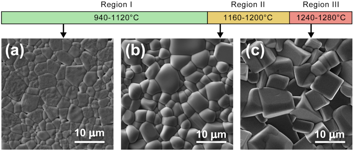
The observed character of the thermally treated surfaces of NBT-Eu samples allow us to divide the thermal treatment temperature range into three regions, as shown in
Figure 1. Region I is the widest, extending from the lowest treatment temperature in our study, 940 °C, up to 1120 °C. SEM micrographs in this region illustrate a microstructure with an almost flat surface, fully packed with grains separated by narrow grain boundaries, which should be expected for dense ceramics (
Figure 1a). Remarkably, the grain boundaries are well distinguishable even at the lowest treatment temperature (940 °C). Region II is much narrower—from 1160 °C to 1200 °C. Here, well-developed relief appears. However, the surface still maintains continuality and grain boundaries are visible (
Figure 1b). Apparently, while the material efficiently sublimates only at the grain boundaries in Region I, more active sublimation leads to widening of the etched area in Region II. The situation changes significantly in Region III—starting from 1240 °C. Regular, square-shaped faces with rounded edges start to appear from an uneven surface already at a lower temperature—1200 °C. Upon an increase in thermal treatment temperature (up to 1240 °C and higher), these faces, oriented in various directions, extend deeper into the surface, creating a cube-like pattern, while the edges of the grains become sharper (
Figure 1c). XRD pattern and EDX scanning over such a surface confirm that, in spite of the specific microstructure obtained at high thermal treatment temperatures, the grains correspond to NBT-Eu—neither changes in lattice symmetry in XRD patterns nor deviations in concentrations of chemical elements in EDX analysis were detected. At 1280 °C, clear signs of partial melting appear. From our point of view, these three types of microstructure, observed at the three thermal treatment temperature regions, correspond well to the three types of microstructure, which are presented in the literature and discussed in the Introduction.
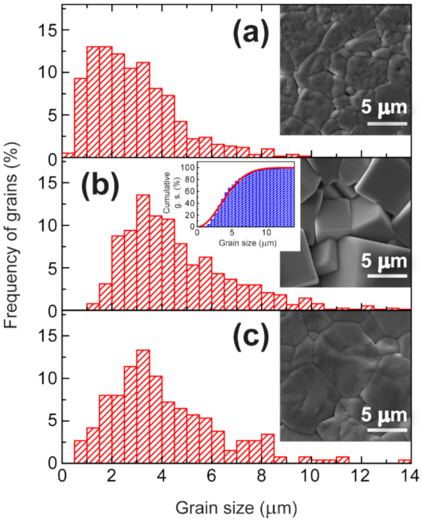
As it follows from the obtained SEM micrographs, the grain size on the surface in Region III obviously increases. It is known that increasing sintering temperature induces an increase in the grain size of the whole ceramic [
25]. Therefore, when analysing the role of thermal treatment temperature in the grain size distribution on the surface, the impact of thermal treatment temperature on the grain size in the bulk of the ceramics cannot be excluded. In order to compare the impact of high treatment temperatures on the grain size in the bulk of the ceramics with the impact on the surface, a surface layer was grinded off after thermal treatment at a high temperature (1240 °C), and another thermal treatment was performed at 980 °C, which presumably does not influence microstructure both on the surface and in the bulk of the ceramics, thus helping to reveal the contribution from the high thermal treatment temperature on the grains in the bulk of the ceramics. The microstructure obtained for the surface thermally treated only at 980 °C was used as a reference. In
Figure 2, it can be seen that the maximum of the grain size distribution, as well as the average grain size, shifted to the larger grain sizes both for the surface thermally treated at 1240 °C (
Figure 2b) and for the bulk of the same ceramic sample—represented by the surface after grinding off the surface layer thermally treated at 1240 °C (
Figure 2c). Thus, we can infer that thermal treatment at high temperatures (Region III) indeed induces remarkable grain growth in the whole ceramics. Comparison of the histograms presented in
Figure 2b,c should be carried out with caution, because the distribution of grain size, obtained for a plane (two-dimensional) surface, in general, does not correspond to the distribution of sizes of real (three-dimensional) grains, except the cases for when the distribution of real grain sizes corresponds to the Rayleigh formula [
26]. Indeed, the grain size distribution obtained from micrographs like the one presented in
Figure 2b roughly corresponds to the Rayleigh distribution (inset in
Figure 2b), which allows us to compare the histograms in
Figure 2b,c, at least qualitatively. Such a comparison reveals a higher frequency of grains at the side of small grains of the grain size distribution in the case of
Figure 2c. It can be assumed that the grain growth on the surface consumes small grains more efficiently than in the bulk of the ceramics.
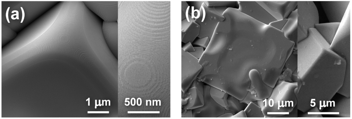
The transformation of the grains into simple geometric shapes is apparently related to the high symmetry of natural faces of NBT-based compositions. At higher SEM magnification, a terrace pattern can be observed on the rounded edges of such regular grains (
Figure 3a). Such a behaviour resembles the usual growth conditions of single crystals: natural faces develop in directions in which crystal growth is slower. Since terraces are observed only on the rounded edges of grains, this transformation reduces the surface of the grains in the direction of low symmetry, extending the high symmetry planes. This is seen on the surface of the sample treated at 1280 °C. The edges of grains in this case are much sharper, in spite of the partial melting observed in some regions of the surface (
Figure 3b).
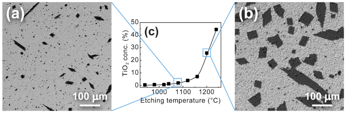
Increasing thermal treatment temperature has one more consequence. Earlier, we observed inclusions on the surface of nominally stoichiometric NBT ceramics. These inclusions appeared to be of a darker shade, compared with the matrix grains, in SEM micrographs obtained in the back-scattered electron (BSE) mode [
26]. EDX investigation suggested that the composition of these inclusions is TiO
2. We have observed the same inclusions in the present study (as indicated by their shape and supported by EDX results). Upon increasing the thermal treatment temperature, their concentration and size on the surface of NBT-Eu ceramics increases (
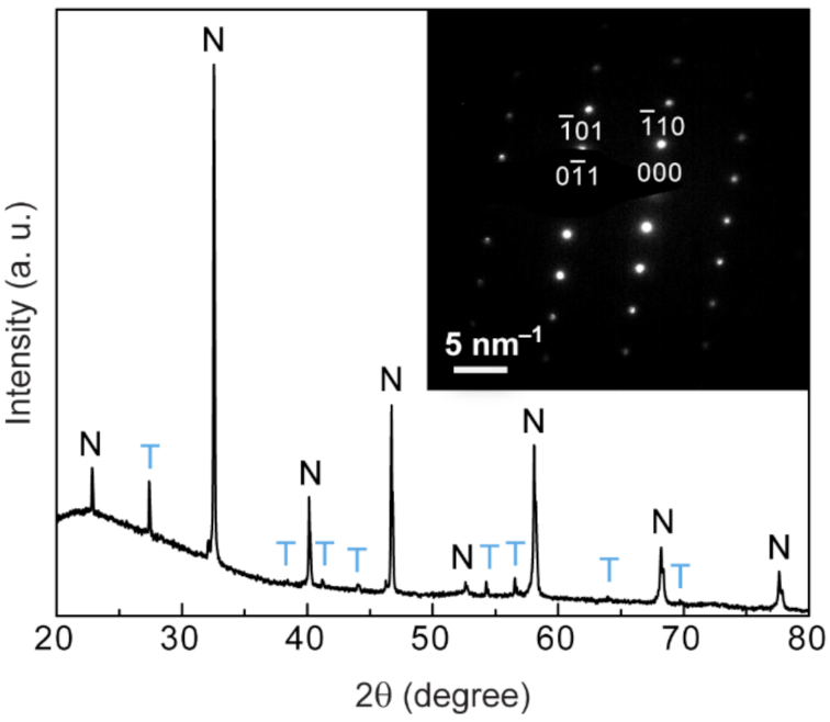
Figure 4). Although irregularly shaped inclusions are observed by SEM on the surface of the non-treated NBT-Eu, their concentration is too low to be detected by XRD. However, after thermal treatment at high temperatures, this concentration on the surface increases significantly, and XRD measurements indicate a clear presence of TiO
2 rutile (
Figure 5). In order to make sure that the inclusions of the non-treated sample are of the same phase, a lamella was cut out and the selected area electron diffraction (SAED) was performed by TEM. The obtained results indicate a crystalline structure, and the diffraction pattern corresponds to TiO
2 rutile along the [111] zone axis (Inset in
Figure 5).
The increase in the inclusion concentration is obviously related to the evaporation of Bi and Na at high temperatures, and the decomposition of NBT-Eu. Increasing the size of TiO
2 inclusions could mean that this process occurs mainly at TiO
2 and NBT-Eu interfaces. It seems that the small inclusion concentration observed at low thermal treatment temperatures characterizes the concentration of TiO
2 in the bulk of the ceramics [
25], which is not related to thermal treatment. These inclusions could be considered as seeds, which grow if thermal treatment at increased temperatures is applied. At the same time, such a kind of NBT decomposition is possible only from a surface layer, while the concentration of TiO
2 inclusions in the bulk does not increase upon increasing sintering temperature [
25]. This reflects significantly different conditions between the surface and the bulk of the ceramics with respect to Na and Bi volatilization—where, instead of increasing TiO
2 inclusion concentration, only the formation of large pores is observed at high sintering temperatures [
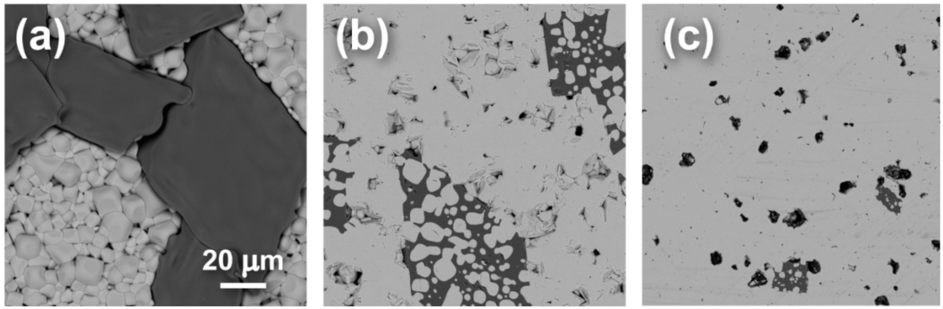
25]. This difference becomes understandable in the context of the present results; as a result of Na/Bi evaporation from the surface layer at high temperatures, the decomposition of NBT takes place instead of generating A-sublattice vacancies, and these elements in the bulk of the ceramics remain captured. Differences between the surface and the deeper layers of the ceramics can be clearly demonstrated by removing the surface layer. We observed that if the distance from the surface increases, the concentration of TiO
2 inclusions decreases, with NBT-Eu grains penetrating into TiO
2, and finally reduces until the inclusion concentration characteristic for the bulk is achieved (
Figure 6).
For one of the thermal treatment temperatures belonging to Region II, namely 1200 °C, the role of thermal treatment time in microstructure was evaluated. Three thermal treatment times were chosen: 0.5 h, 1 h, and 2 h. The comparison of the micrographs obtained for all three treatment times did not reveal any detectable changes in the average grain size and grain size distribution. At the same time, an increasing TiO2 inclusion concentration was observed.
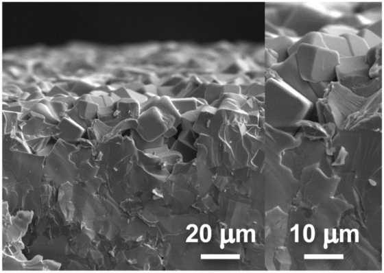
Of course, we cannot exclude the existence of other methods, even accidental, of obtaining the microstructure of the third type (observed in thermal treatment temperature Region III). The term “microstructure of ceramics” is not applicable in this case, even in general assumptions, if dense ceramics are considered. The absence of a more or less flat surface with grain boundaries and a remarkable concentration of empty spaces between the faces of grains clearly reveals a loose structure (such cubic-shaped grains, oriented in various directions, cannot create dense packing also in general assumptions), while the fraction of the small grains is significantly reduced compared with the bulk of the ceramics. The non-compliance of such a micrograph with the actual microstructure follows not only from the comparison of grain size distribution (
Figure 2b,c). It can be clearly demonstrated also visually, when considering the microstructure of a cross section (fracture) of the thermally treated sample. As can be seen from
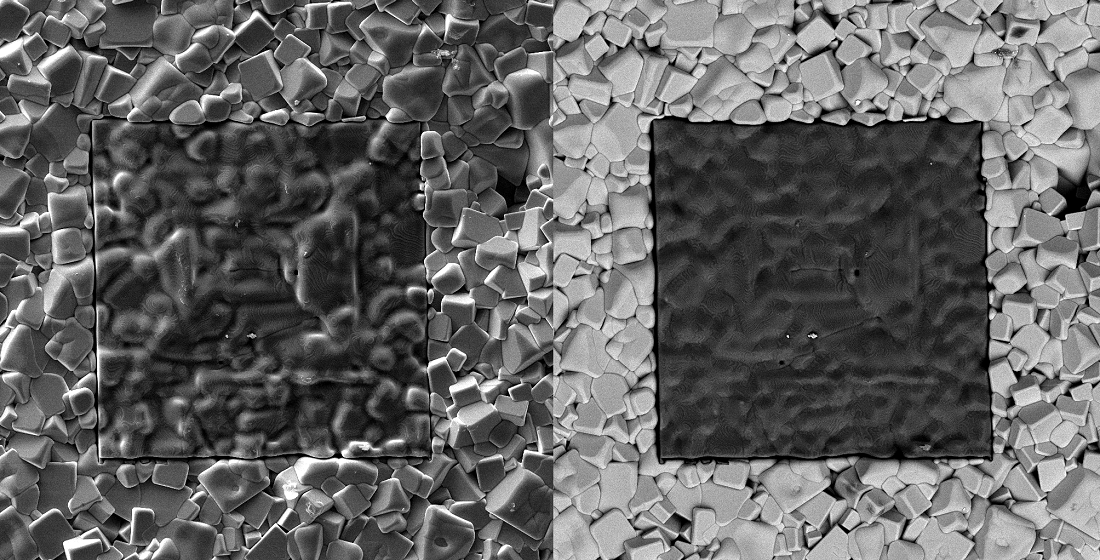
Figure 7, only the thermally treated surface has the specific microstructure of the third type, while, beneath the surface layer, the ceramic is dense.
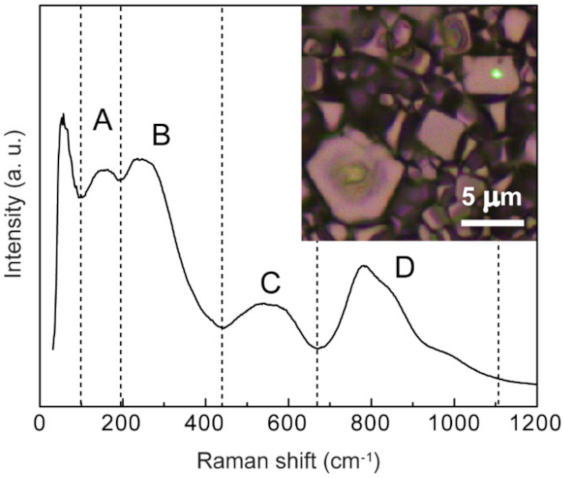
The micrographs belonging to the third type can be valuable, even though they do not represent the real microstructure and are not appropriate for the characterisation of the microstructure. First of all, they clearly reveal very symmetric natural faces of NBT-Eu grains, which allows one to explain the grain growth mechanism in NBT-based ceramics [
3]. They also indicate that individual grains in NBT-Eu ceramics are single crystals of a simple symmetry. In addition, sometimes they can be used to study the properties of appropriately oriented single crystals. As an example, we performed micro-Raman investigation for a single grain oriented in the [100] direction of the ceramics thermally treated at 1240 °C (inset in
Figure 8). The obtained spectrum is presented in
Figure 8. Its specific character is additional evidence of the fact that crystals, which grow on the surface of the sample in heavy thermal treatment conditions, are pure NBT-Eu. Four broad bands in the ranges of 100–150 cm
−1, around 250 cm
−1, 500–600 cm
−1, and around 800 cm
−1 correspond to the well-known Raman spectrum in NBT [
27].


