
Silica Microspheres for Economical Advanced Solar Applications


Materials Science Research Institute, King Abdullaziz City for Science and Technology (KACST), P.O. Box 6086, Riyadh 11442, Saudi Arabia
Crystals 2021, 11(11), 1409; https://0-doi-org.brum.beds.ac.uk/10.3390/cryst11111409
Submission received: 30 September 2021
/
Revised: 5 November 2021
/
Accepted: 15 November 2021
/
Published: 18 November 2021
(This article belongs to the Special Issue Fabrication of Carbon and Related Materials/Metal Hybrids and Composites)
Abstract
:Solar cells made of silicon nanowires (Si-NWs) have several potential benefits over conventional bulk Si ones or thin-film devices related primarily to light absorption and cost reduction. Controlling the position of Si-NWs without lithography using silica microspheres is indeed an economical approach. Moreover, replacing the glass sheets with polycarbonates is an added advantage. This study employed the Nanoscale Chemical Templating (NCT) technique in growing Si-NWs seeded with Al. The growth was undertaken at the Chemical Vapor Deposition (CVD) reactor via the original growth process of vapor–liquid–solid (VLS). The bottom-up grown nanowires were doped with aluminum (Al) throughout the growth process, and then the p–n junctions were formed with descent efficiency. Further work is required to optimize the growth of Si-NWs between the spun microspheres based on the growth parameters including etching time, which should lead to more efficient PV cells.
1. Introduction
Conventional 3D crystal growth requires only two phases; however, nanowires grow in three-phase systems. The vapor–liquid–solid (VLS) mechanism is based on systems that combine three phases: a vapor that supplies the materials for crystal growth, a liquid droplet to seed the growth, and the solid crystal. One-dimensional crystal (NWs) growth occurs when the growth rate at the interface between the liquid phase and the solid crystal is higher than the growth rate at the interface between the vapor/solid phase boundary.
Vertical NWs made of silicon substrate are of great interest because they would allow for ultimate light trapping and distinguished charge carriers’ separation for solar cell applications. They could therefore achieve, in principle, better efficiency than thin-film planar cells, with the added merits of minimal use of materials and much lower process cost [1]. Nanowire solar cells have some potential benefits over traditional wafer-based or thin-film devices related to optical, electrical, and strain relaxation effects, charge separation mechanisms, and cost reduction. Ordered arrays of vertical nanowires with radial junctions take advantage of all these effects, as explained in some detail by Wacaser et al. [2]. Controlling the position of nanowires is another important topic for research. A promising emerging field for future low-cost, decent efficiency solar cell devices is the use of vapor–liquid–solid (VLS)-grown Si-NWs. The bottom-up approach of Si-NW growth via the VLS mechanism has a key advantage for device applications, since it is possible to template the position of the NWs by controlling the placement of the initial metal seed or catalyst particle. This templating then allows the integration of NWs with other parts of the structure, as required for many of these applications [3,4,5,6]. The technique of microsphere lithography has been proposed to produce regular hexagonal arrays of Al-seeded nanowires, and the fabrication process continues to fabricate solar cells [5,6,7,8]. Templating the Si-NWs’ growth has been explained by several research groups [1,2,6,9,10,11], using wide schemes of techniques including electron beam lithography. Employing microspheres to template the growth of NWs will reduce the production cost of device fabrication; however, this area of research requires further investigations. The current study is a direct application of the concept of Nanoscale Chemical Templating (NCT) [6]. There are several advantages of using microspheres at the level of templating the growth, as it is an economical approach that reduces the number of the required steps of lithography. Moreover, using polycarbonate sheets in solar cells is a potential application. According to the SABIC report, there is a 61% CO2 footprint reduction for each Kg of polycarbonate based on certified renewable feedstock [9]. Polycarbonate plastic materials are transparent amorphous, although they are made commercially available in a variety of colors, and the raw material allows for the internal transmission of light nearly in the same capacity as glass. Polycarbonate polymers are used to produce a variety of materials and are particularly useful when impact resistance or transparency is a product requirement. Polycarbonate is a relatively hard, lightweight material. These properties make polycarbonates suitable for products intended for long open-air operation, such as PV cells and modules.
2. Experiments
A Chemical Vapor Deposition (CVD) reactor has been used to grow Si-NWs via the VLS process, which includes a home-built Al evaporator operated under Ultra High Vacuum (UHVCVD). Si-NWs, as previously observed [5,7], grow preferentially 45° tilted on Si (100), and perpendicularly in the (111) direction, so Si (111) substrates were primarily used. The detailed general growth conditions along with the pre-growth steps were described in previous studies [5,6,7,8].
The thickness of the Al catalyst layer is of critical importance to the grown NWs. As the thickness of the seed Al increases from 2 nm to 5 nm, the fidelity of the growth increases, then after reaching 5 nm Al thickness the growth fidelity decreases quite significantly. Based on these measurements, it has been decided to choose 5 nm of Al thickness. The samples were then transferred into the hot growth chamber for a pre-growth anneal at 600 °C, which is above the Al/Si bulk eutectic temperature of 577 °C. This anneal was for 20 min under full pumping and was intended to allow the Al film to agglomerate into small islands on the surface and ball up, forming liquid droplets. The furnace was then cooled to the desired growth temperature (usually 520 °C), and pure silane (SiH4) was introduced at a fixed flow, 20 sccm, using a mass flow controller (MFC). The morphology of grown Si-NWs was examined with an environmental scanning electron microscope (SEM) FEI Co., Eindhoven, The Netherlands, model XL 30.
Silica microspheres are commercially available with narrow size distributions and have an average diameter of less than 1 µm (approximately 900 nm). When silica microspheres are dispersed properly using a spinner on the Si substrate surface, they form a close-packed array that forms gaps through which a material can be deposited. Si (111) of p-type substrates were cleaned using standard techniques [5,6,7,8,9,10,11], which leave a thin oxide on the Si surface. A drop of 1 μm diameter polystyrene microspheres in solution taken directly from the commercially provided stock solution was dispersed onto the substrate.
Reflectance measurements were undertaken using the F10-RT reflectometer, which captures reflectance and transmittance simultaneously (sample thickness range 15–1000 µm, wavelength range 200–900 nm). I-V characteristics were carried out using “keithley 2400” source meter.
3. Results and Discussion
The current experimental work is focused on using the economic approach using microspheres for templating the growth of nanowires (Section 3.1.1.). We assessed the light reflectance and I-V characteristics of Si-NWs (Section 3.1.2).
3.1. Controlling the Growth Position of Si-NWs
Controlling the growth position of Si-NWs, catalyzed with Al, can be undertaken using e-beam lithography [6,7].
3.1.1. Templating Si-NWs Using Polystyrene Microspheres and SiO2 Thin-Layer Lithography
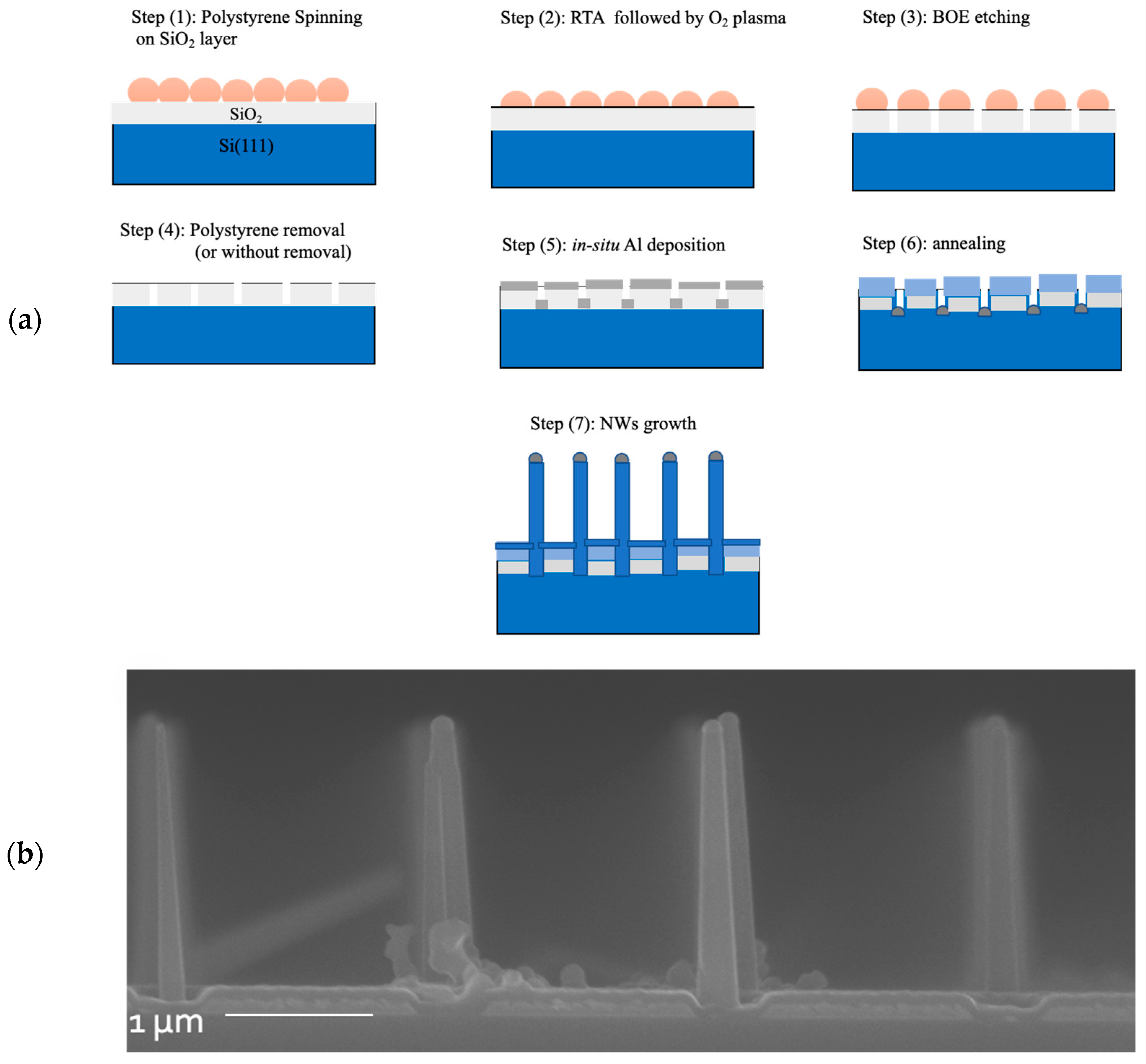
The concept of the NCT technique has been explained and employed, as shown in Figure 1. A schematic illustration of the NCT process in seven main steps is presented in Figure 1a as follows: Step (1) starts off with Si (111), where nanowires grow perpendicularly, which includes a thin layer of SiO2 (approximately 50 nm), where polystyrene microspheres are spun on it. Step (2): In oxygen plasma, Rapid Thermal Annealing (RTA) is performed. Step (3) involves etching using BOE, and then the removal of polystyrene microspheres occurs in step (4), or the process could continue without the removal of the microspheres. Step (5) involves the deposition of a 5 nm thick layer of Al on the surface covering the top surfaces of the microspheres and bare Si surface. Step (6) is where annealing is undertaken, showing that Al on the top of SiO2 oxidizes, forming Al2O3, or on the top of the microspheres (if they have not been removed), and the Al in the opening balls up. Then, in step 7, the growth of Si-NWs occurs after allowing SiH4 to flow, providing the required medium of the VLS system. The epitaxial perpendicular Si-NW growth of approximately 2 µm long is accompanied by the planar deposition of Si of a few nanometers between Si-NWs (see Figure 1b) [12].
3.1.2. Templating Si-NWs Using Silica Microsphere Lithography
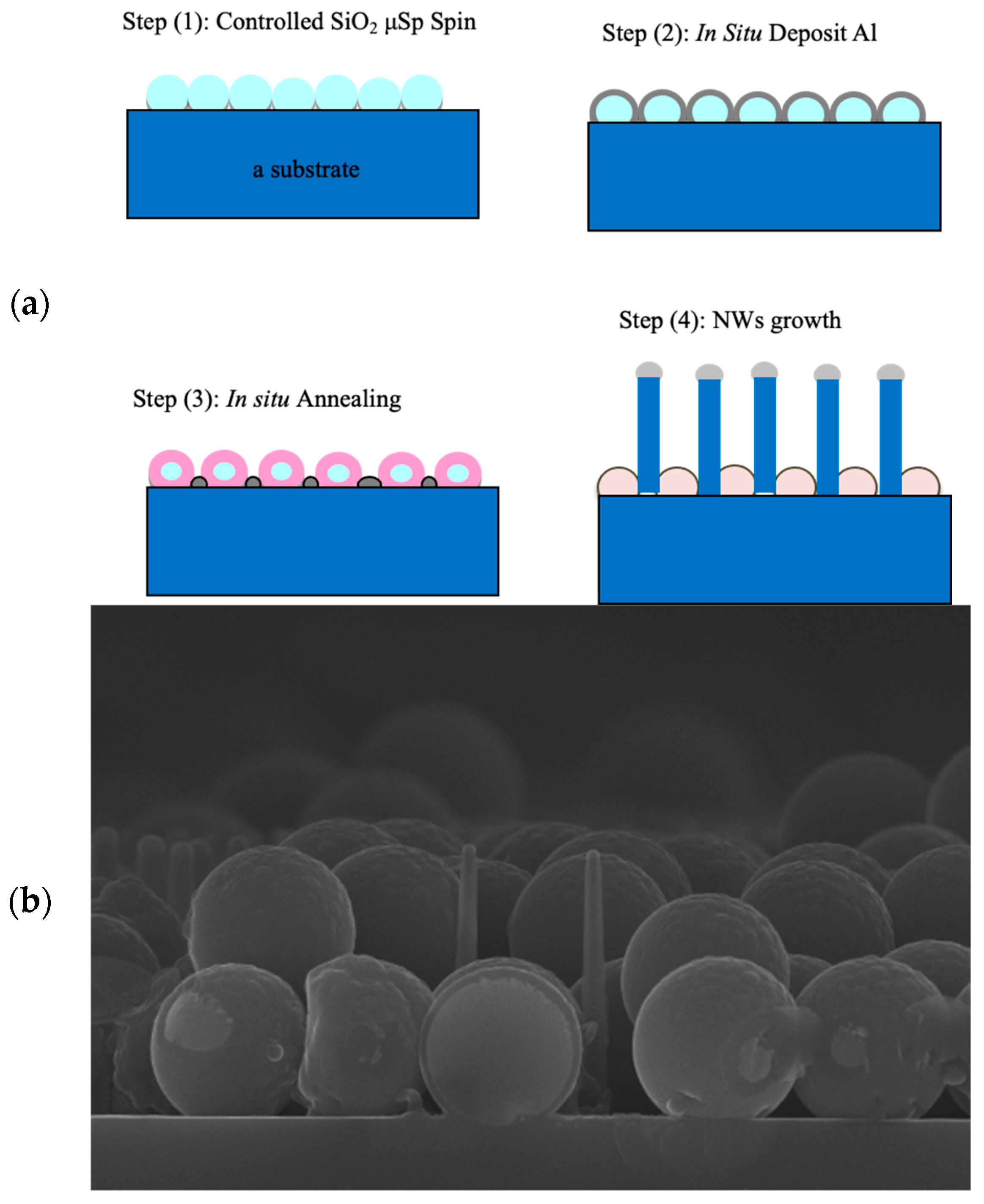
The concept of the original process of the NCT technique explained schematically in Figure 1 can be employed in fewer steps, as presented in Figure 2. After careful spinning of silica microspheres that are commercially available with narrow size distributions (step 1), in step 2, the oxide is etched with buffered oxide etch solution (BOE 9:1 Seidler Chemical Company; 9 parts 40% NH4F in water to 1 part 49% HF in water), typically for a few seconds. Then, annealing (step 3) is followed by NW growth, as explained earlier [5,7].
The described concept in Figure 2 has been examined and it showed encouraging results; however, further optimization of the Si-NWs’ growth has to be carried out. It can be shown that the outer shell of the silica microspheres appears in a different color, confirming that the evaporated Al on the outer surfaces of the silica microsphere has been oxidized, forming Al2O3 on the top of it. A thin unseeded planar Si layer forms on the surface of the microspheres, just as for the standard lithography case. We found that the gaps between microspheres could be controlled to some extent by varying the BOE time. If etch times exceeding 10 s were used, the gaps became large enough for NWs to be seeded in the openings. However, etch times longer than 45 s resulted in some of the microspheres lifting off the Si surface to leave large gaps where multiple nanowires could grow. This process has not been optimized for yield.
Si (NWs) will not grow on these microspheres due to the oxidation of the Al catalysts. We show the results of this process, where Si-NWs can be seen growing in the gaps between the microsphere array, where the Al catalyst is on the Si substrate. The microspheres of silica exhibit two main contents of distinct colors. The core, which represents more than 90% of the microsphere, remains as it is, while on the very outer exposed part of the shell of oxidized Al, a thin unseeded planar Si layer forms on the surface of the microspheres, just as for the standard lithography case. We found that the gaps between microspheres could be controlled to some extent by varying the BOE time. If etch times longer than 10 s were used, the gaps became large enough for NWs to be seeded in the openings. However, etch times longer than 45 s resulted in some of the microspheres lifting off the Si surface to leave large gaps where multiple nanowires could grow. This process has not been optimized for yield. Khan et al., in 2015 and 2016 [13,14], respectively, reported that liquid nanodroplets Indium Nanodroplets (In NDs) act as facilitator sites for Si deposition. These nano-sized droplets can be considered as the growth catalyst and it is part of the produced device, just like Al in our work. However, our work used silica microspheres, which can be removed after templating the growth or could stay there between the grown nanowires as an electrical insulator for several applications such as the MOSFETs and photovoltaic (PV) cells.
3.2. Light Absorption of Si-NWs and PV Applications
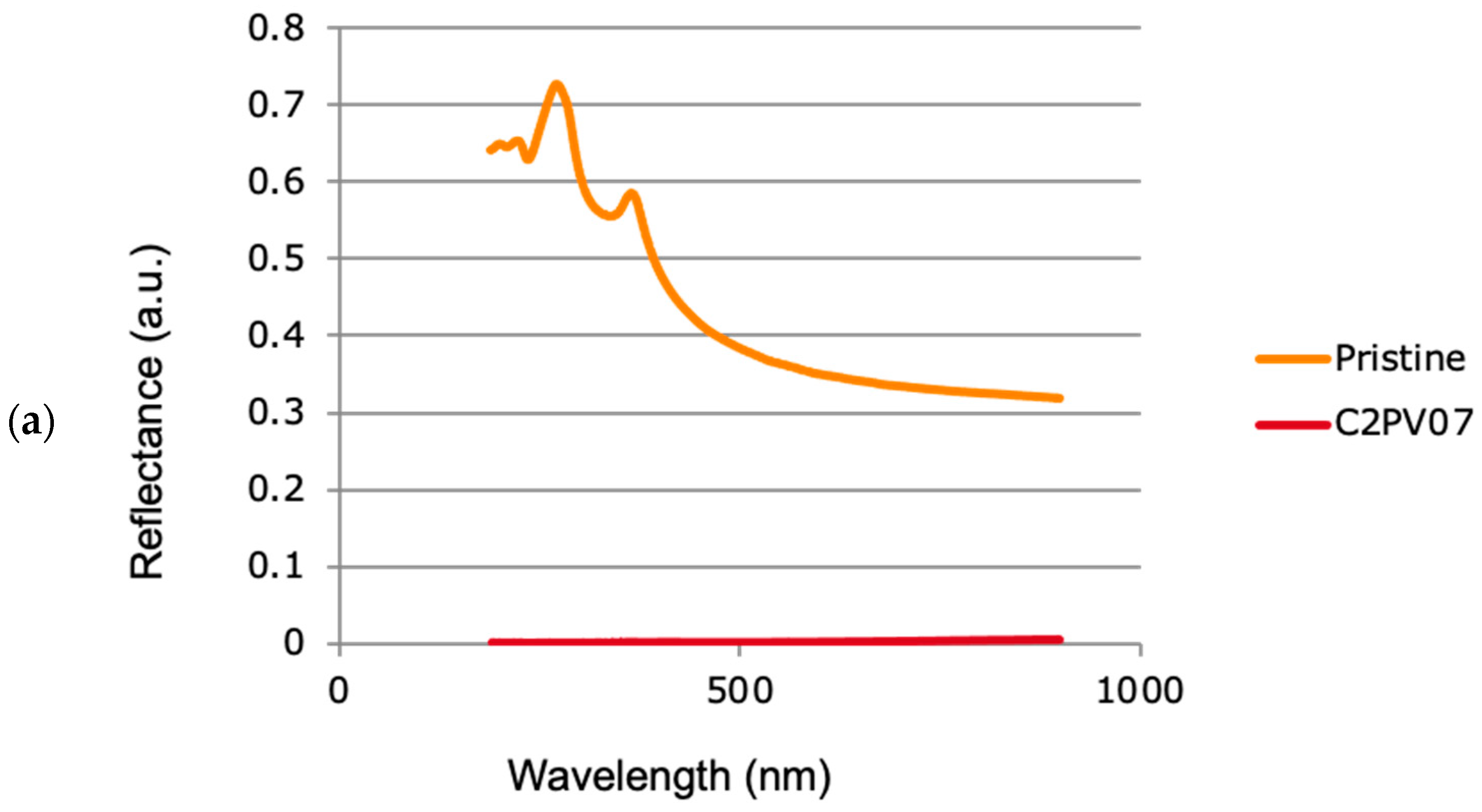
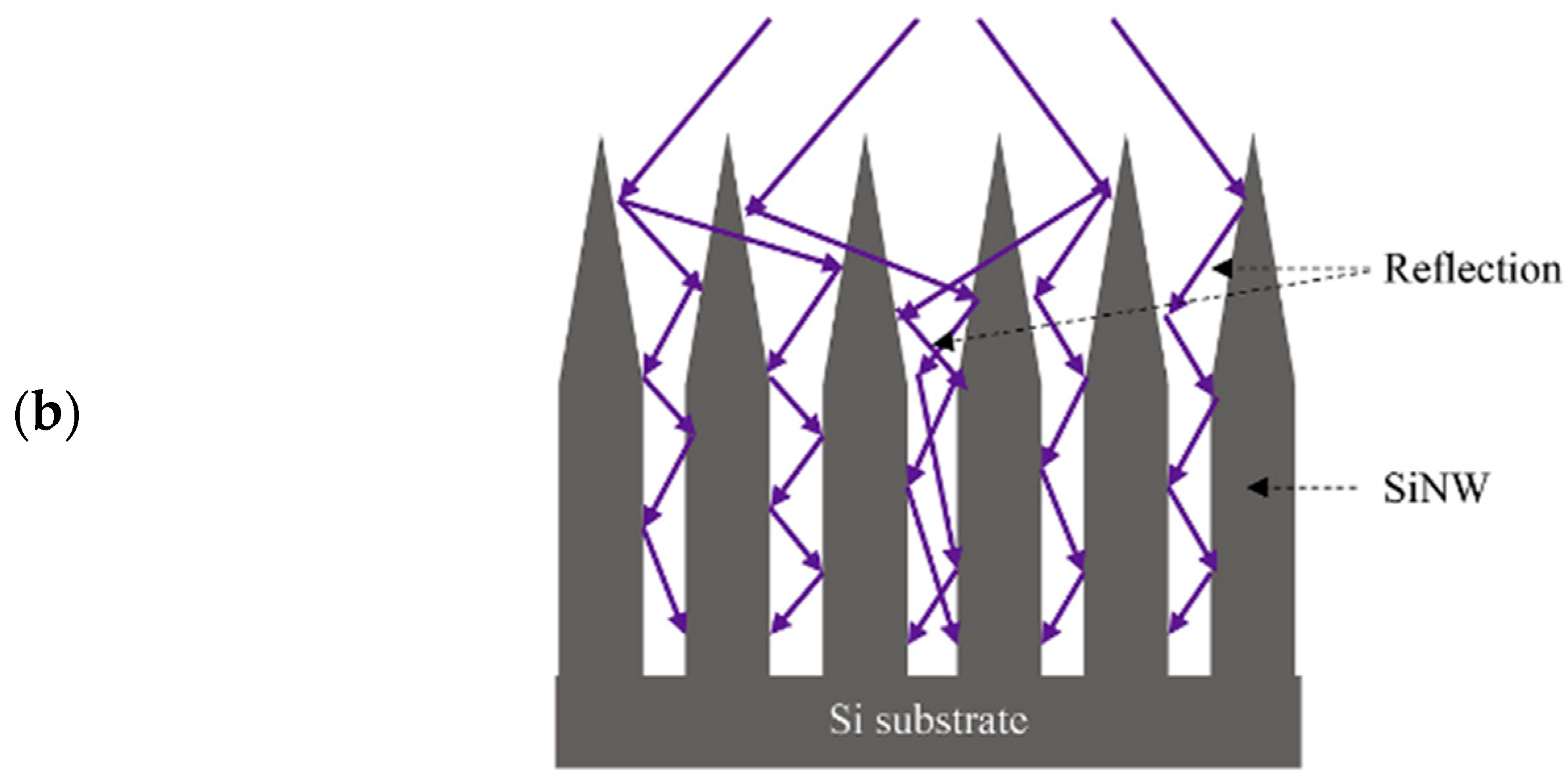
Nanowires have a very high surface to volume ratio, making them ideal components for light absorption or any related interface phenomena. The optical characteristics of Si-NWs exhibit excellent light harvesting characteristics (see Figure 3). The reflectance of light from the Si substrate covered with NWs is almost zero, in comparison to the pristine Si substrate, as shown in Figure 3a. The schematic illustration is presented in Figure 3b, describing how the light rays are reflected between the NWs, increasing the chance of absorption of the incident light rays [15,16,17].
Growing semiconductor nanowires can be catalyzed by chemically active materials using an efficient and economic approach. It has been well established in the literature that nanowires can be catalyzed using gold (Au). However, gold negatively affects the performance of semiconductor devices, as it acts as a deep-level trapping charge carrier. On the other hand, Al is a part of the semiconductor industry, as it is used as p-type dopants of silicon. However, Al is a chemically active element; as we deposit aluminum on the semiconductor substrate, we should not expose the samples to air, so the NCT technique can be employed. It is possible to form the p–n core–shell junctions in high-density arrays, which have the benefit of decoupling the absorption of light from charge transport by allowing lateral diffusion of minority carriers to the p–n junction, which is at most 50–500 nm away rather than many microns away as in Si bulk solar cells [18,19,20]. Based on this, the potential cost benefits come from lowering the purity standard and the amount of semiconductor material needed to obtain sophisticated efficiencies, increasing the defect tolerance, and lattice-matched substrates. The concept of NW-based PV cells has attracted the scientific community’s attention because of their potential benefits in carrier transport, charge separation, and light absorption [21]. The Lieber [11,19] and Atwater [9,10] and other groups [10,22,23,24] have developed core–shell growth and contact strategies for their silicon p–n nanowire solar cells, with sophisticated efficiencies. After all, Si-NWs possess the combined attributes of cost effectiveness and mature manufacturing infrastructures for further advanced applications. Increasing the growth temperature increases the active doping of Al-catalyzed NWs.
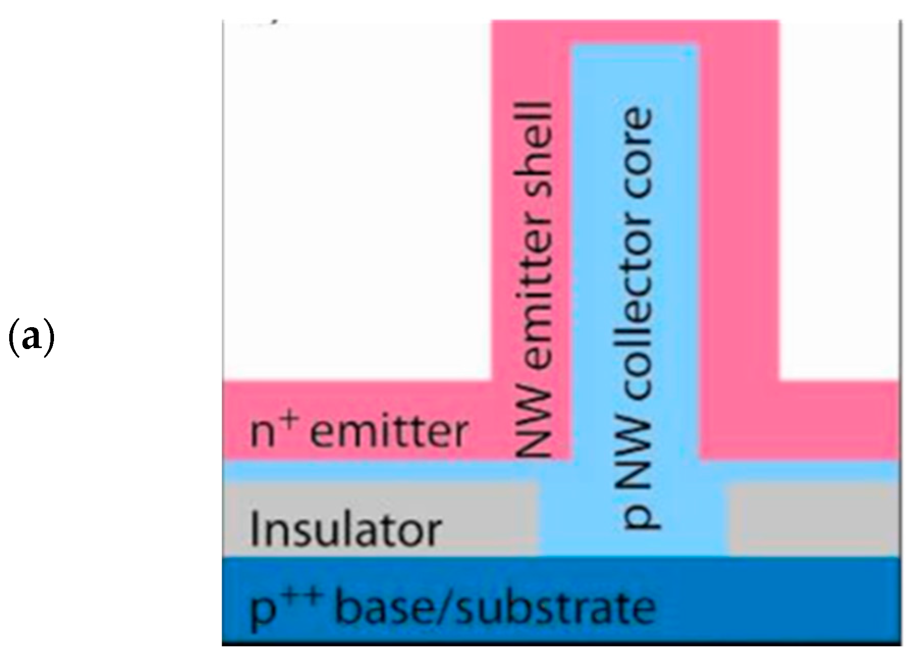
Thicker lightly doped NWs and doping the outer areas by diffusion are shown in Figure 4a. The width of the junction can be engineered, if required, by controlling the width of the intrinsic layer, forming a p–i–n junction [22,23,24].
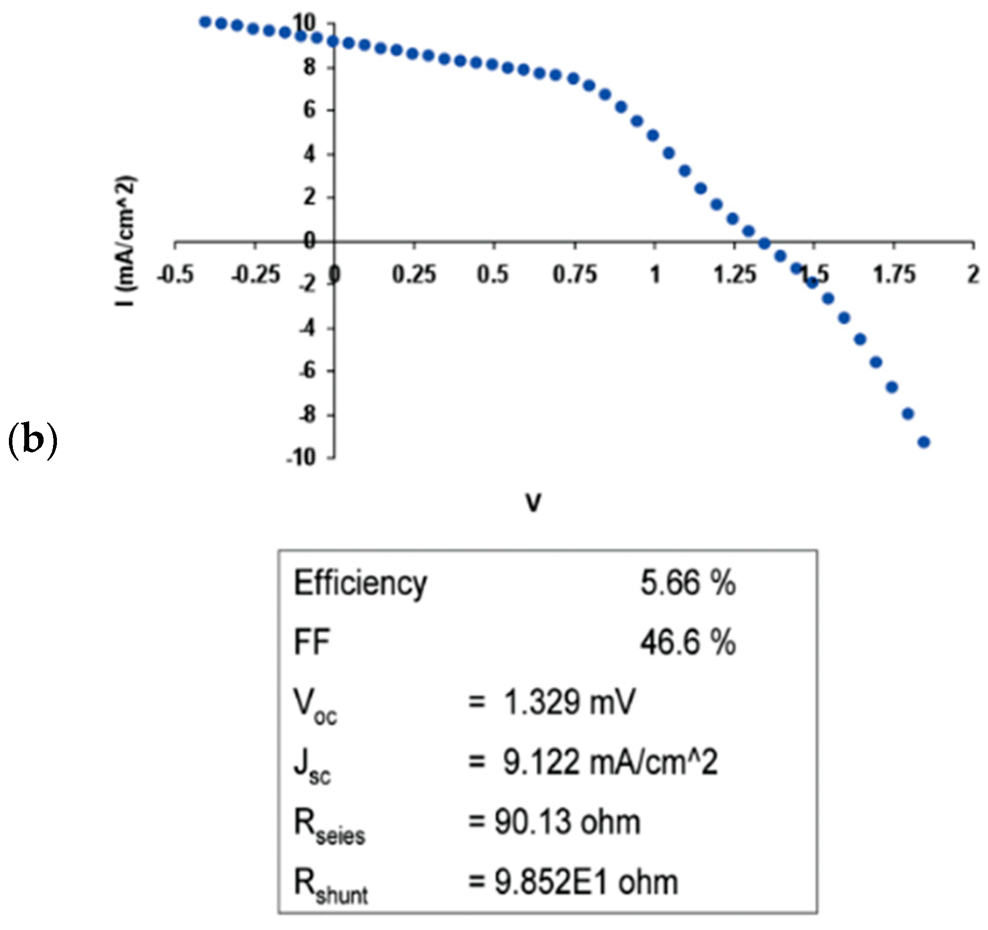
The obtained electrical efficiency of the fabricated PV showed encouraging results of 5.66%, along with the other related parameters, as shown in Figure 4b. Clearly, much work is required to improve the performance of the PV cell made of Si-NWs. Forming an ideal p–n junction for core–shell NWs by CVD is not a trivial undertaking. Typically, when switching precursors in CVD, much care is needed to keep from forming defects at the interfaces. This problem is only compounded by the NWs because they have a three-dimensional shape with different facet orientations and characteristics. The engineering of this interface is an ongoing research topic that will need to be resolved to make core–shell grown nanowires competitive for large-scale PV [23,24,25].
4. Conclusions
The combination of the NCT technique along with silica microspheres is an economic approach, as it requires fewer steps compared to conventional patterning approaches, not requiring lift off of a metal layer or the removal of the mask. The encapsulation of silicon solar panels with PC sheets reduces the weight of the solar panels and opens up more applications of solar panels in harsh environments considering the mechanical properties of PC. The methodology used in achieving the controlled placement of single NWs seeded with Al is an example of proving the concept of the NCT technique; however, more detailed work is required to optimize the growth process and increase the NWs’ growth fidelity, leading to more efficient PV cells. More oxygen-reactive materials such as Sn, Sb, In, Ga, and Ti templated by NCT will have more advanced applications in nanodevice fabrications.
Funding
This research has been conducted as part of the employment at KACST.
Institutional Review Board Statement
Not applicable.
Informed Consent Statement
Not applicable.
Data Availability Statement
The data used to support the findings of this study are included within the article.
Acknowledgments
The author would like to thank T. C. Chen of the T. J. Watson Research Center, IBM, Yorktown Heights, NY, for his scientific insights throughout working on this project.
Conflicts of Interest
The author declares that there is no conflict of interest regarding the publication of this paper.
References
- Kim, J.; Hong, A.J.; Nah, J.-W.; Shin, B.; Ross, F.; Sadana, D.K. Three-Dimensional a-Si:H Solar Cells on Glass Nanocone Arrays Patterned by Self-Assembled Sn Nanospheres. ACS Nano 2011, 6, 265–271. [Google Scholar] [CrossRef]
- Wacaser, B.; Khayyat, M.; Reuter, M.; Sadana, D.; Ross, F. Technical advantages and challenges for core-shell micro/nanowire large area PV devices. In Proceedings of the 2010 35th IEEE Photovoltaic Specialists Conference, Honolulu, HI, USA, 20–25 June 2010. [Google Scholar]
- Huang, B.; Lin, T.; Hung, W.; Sun, F. Performance evaluation of solar photovoltaic/thermal systems. Sol. Energy 2001, 70, 443–448. [Google Scholar] [CrossRef]
- Gong, L.; Lu, J.; Ye, Z. Transparent and conductive Ga-doped ZnO films grown by RF magnetron sputtering on polycarbonate substrates. Sol. Energy Mater. Sol. Cells 2010, 94, 937–941. [Google Scholar] [CrossRef]
- Wacaser, B.; Reuter, M.C.; Khayyat, M.; Wen, C.-Y.; Haight, R.; Guha, S.; Ross, F. Growth System, Structure, and Doping of Aluminum-Seeded Epitaxial Silicon Nanowires. Nano Lett. 2009, 9, 3296–3301. [Google Scholar] [CrossRef] [PubMed]
- Khayyat, M.; Wacaser, B.; Reuter, M.; Ross, F.; Sadana, D.; Chin, T. Nanoscale chemical templating of Si-NWs seeded with Al. Nanotechnology 2013, 24, 235301. [Google Scholar] [CrossRef]
- Khayyat, M.; Wacaser, B.; Sadana, D. Nanoscale Chemical Templating with Oxygen Reactive Materials. U.S. Patent Number 8349715, 2013. [Google Scholar]
- Fan, H.J.; Werner, P.; Zacharias, M. Semiconductor Nanowires: From Self-Organization to Patterned Growth. Small 2006, 2, 700–717. [Google Scholar] [CrossRef]
- Kayes, B.M.; Atwater, H.A.; Lewis, N.S. Comparison of the device physics principles of planar and radial p–n junction nanorod solar cells. J. Appl. Phys. 2005, 97, 114302. [Google Scholar] [CrossRef]
- Kayes, B.M.; Filler, M.A.; Putnam, M.C.; Kelzenberg, M.D.; Lewis, N.S.; Atwater, H.A. Growth of vertically aligned Si wire arrays over large areas (>1 cm2) with Au and Cu catalysts. Appl. Phys. Lett. 2007, 91, 103110. [Google Scholar] [CrossRef] [Green Version]
- Huang, Y.; Lieber, C.M. Integrated nanoscale electronics and optoelectronics: Exploring nanoscale science and technology through semiconductor nanowires. Pure Appl. Chem. 2004, 76, 2051–2068. [Google Scholar] [CrossRef]
- Wagner, R.S.; Ellis, W.C. Vapor-liquid-solid mechanism of single crystal growth. Appl. Phys. Lett. 1964, 4, 89–91. [Google Scholar] [CrossRef]
- Khan, M.A.; Ishikawa, Y.; Kita, I.; Fukunaga, K.; Fuyuki, T.; Konagai, M. Control of verticality and (111) orientation of In-catalyzed silicon nanowires grown in the vapour–liquid–solid mode for nanoscale device applications. J. Mater. Chem. C 2015, 3, 11577–11580. [Google Scholar] [CrossRef]
- Khan, M.A.; Ishikawa, Y.; Kita, I.; Tani, A.; Yano, H.; Fuyuki, T.; Konagai, M. Investigation of crystallinity and planar defects in the Si nanowires grown by vapor–liquid–solid mode using indium catalyst for solar cell applications. Jpn. J. Appl. Phys. 2015, 55, 01AE03. [Google Scholar] [CrossRef]
- Kim, H.; Bae, H.; Chang, T.-Y.; Huffaker, D.L. III–V nanowires on silicon (100) as plasmonic-photonic hybrid meta-absorber. Sci. Rep. 2021, 11, 13813. [Google Scholar] [CrossRef]
- Zeng, W.R.; Li, S.F.; Chow, W.K. Preliminary Studies on Burning Behavior of Polymethylmethacrylate (PMMA). J. Fire Sci. 2002, 20, 297–317. [Google Scholar] [CrossRef]
- Wacaser, B.; Reuter, M.; Khayyat, M.; Haight, R.; Guha, S.; Ross, F. The Role of Microanalysis in Micro/Nanowire-Based Future Generation Photovoltaic Devices. Microsc. Microanal. 2010, 16 (Suppl. S2), 1368–1369. [Google Scholar] [CrossRef] [Green Version]
- Khayyat, M.; Wacaser, B.; Reuter, M.; Sadana, D. Templating silicon nanowires seeded with oxygen reactive materials. In Proceedings of the 2011 Saudi International Electronics, Communications and Photonics Conference (SIECPC), Riyadh, Saudi Arabia, 24–26 April 2011. [Google Scholar]
- Law, M.; Goldberger, J.; Yang, P. Semiconductor nanowires and nanotubes. Annu. Rev. Mater. Res. 2004, 34, 83–122. [Google Scholar] [CrossRef] [Green Version]
- Samuelson, L. Semiconductor nanowires for 0D and 1D physics and applications. Physica E 2004, 25, 313–318. [Google Scholar] [CrossRef]
- Givargizov, E. Fundamental VLS growth. J. Cryst. Growth 1975, 31, 20–30. [Google Scholar] [CrossRef]
- Wacaser, B.; Dick, K.; Johansson, J.; Borgstrom, M.; Deppert, K.; Samuelson, L. Preferential interface nucleation: An expansion of the VLS growth mechanism for nanowires. Adv. Mater. 2009, 21, 153–165. [Google Scholar] [CrossRef]
- Westwater, J.; Gosain, D.; Pand, S. Control of the size and position of silicon nanowires grown via the vapor–liquid–solid technique. Jpn. J. Appl. Phys. 1997, 136, 6204–6209. [Google Scholar] [CrossRef]
- Harper, C.A. Handbook of Plastic Processes; John Wiley & Sons: Hoboken, NJ, USA, 2005. [Google Scholar]
- Lee, C.-L.; Goh, W.-S.; Chee, S.-Y.; Yik, L.-K. Enhancement of light harvesting efficiency of silicon solar cell utilizing arrays of poly(methyl methacrylate-co-acrylic acid) nano-spheres and nano-spheres with embedded silver nano-particles. Photonics Nanostructures-Fundam. Appl. 2017, 23, 36–44. [Google Scholar] [CrossRef]
Figure 1.
(a) A schematic presentation of the original NCT technique, showing that microspheres (MS) can be used for templating in 6 main steps. (b) SEM micrograph of grown Si (NWs) using NCT. See the layers between Si-NWs—the bright layer is SiO2, which is the top surface of it that is oxidized, forming Al2O3, covered by the dark layer of planar growth of Si.

Figure 2.
(a) A schematic representation showing that microspheres (MS) of silica were used for templating in four main steps, along with the side view SEM micrograph of grown Si-NWs between the MS (b). A thin unseeded planar Si layer forms on the surface of the oxidized Al on the outer surface of microspheres (just as for the standard lithography case). The gaps between microspheres could be controlled by varying the BOE time (scale bar is 500 nm).

Figure 3.
Si-NWs are excellent light absorbers. (a) The reflectance of Si-NWs is almost zero in comparison to pristine Si. (b) Schematic representation shows how the light rays bounce between the NWs to be absorbed eventually.
Figure 3.
Si-NWs are excellent light absorbers. (a) The reflectance of Si-NWs is almost zero in comparison to pristine Si. (b) Schematic representation shows how the light rays bounce between the NWs to be absorbed eventually.


Figure 4.
(a) Schematic illustration of p_n junction of Si-NWs, (b) I-V characteristics of the fabricated PV cell of Si-NWs.
Figure 4.
(a) Schematic illustration of p_n junction of Si-NWs, (b) I-V characteristics of the fabricated PV cell of Si-NWs.


Publisher’s Note: MDPI stays neutral with regard to jurisdictional claims in published maps and institutional affiliations. |
© 2021 by the author. Licensee MDPI, Basel, Switzerland. This article is an open access article distributed under the terms and conditions of the Creative Commons Attribution (CC BY) license (https://creativecommons.org/licenses/by/4.0/).
Share and Cite
MDPI and ACS Style
Khayyat, M.M. Silica Microspheres for Economical Advanced Solar Applications. Crystals 2021, 11, 1409. https://0-doi-org.brum.beds.ac.uk/10.3390/cryst11111409
AMA Style
Khayyat MM. Silica Microspheres for Economical Advanced Solar Applications. Crystals. 2021; 11(11):1409. https://0-doi-org.brum.beds.ac.uk/10.3390/cryst11111409
Chicago/Turabian StyleKhayyat, Maha M. 2021. "Silica Microspheres for Economical Advanced Solar Applications" Crystals 11, no. 11: 1409. https://0-doi-org.brum.beds.ac.uk/10.3390/cryst11111409
Note that from the first issue of 2016, this journal uses article numbers instead of page numbers. See further details here.