Article

Substrate Effects on the Electrical Properties in GaN-Based High Electron Mobility Transistors

1
DMC Convergence Research Department, Electronics and Telecommunications Research Institute, Daejeon 34129, Korea
2
Photonic/Wireless Device Research Division, Electronics and Telecommunications Research Institute, Daejeon 34129, Korea
3
LED Business Unit, LG Innoteck, Gyeonggi-do 150721, Korea
4
Foundry Yield Enhancement Team, Samsung Electronics Co. Ltd., Gyeonggi-do 443742, Korea
*
Author to whom correspondence should be addressed.
Submission received: 26 October 2021 / Revised: 16 November 2021 / Accepted: 17 November 2021 / Published: 19 November 2021
(This article belongs to the Special Issue Advances in Gallium Nitride-Based Materials and Devices)

Abstract

:
We report the electrical characteristics of GaN-based high electron mobility transistors (HEMTs) operated on various substrates/films. For the detailed investigation and comparison of the electrical properties of GaN-based HEMTs according to the substrates/films, GaN-based HEMTs were processed using 4-inch sapphire substrates and separated from their original substrates through the laser lift-off technique. The separated AlGaN/GaN films including processed GaN-based HEMTs were bonded to AlN substrate or plated with a 100 µm-thick Cu at the back-side of the devices since AlN substrate and Cu film exhibit higher thermal conductivity than the sapphire substrate. Compared to the sapphire substrate, DC and RF properties such as drain current, transconductance, cut-off frequency and maximum oscillation frequency were improved, when GaN-based HEMTs were operated on AlN substrate or Cu film. Our systematic study has revealed that the device property improvement results from the diminishment of the self-heating effect, increase in carrier mobility under the gated region, and amelioration of sheet resistance at the access region. C(V) and pulse-mode stress measurements have confirmed that the back-side processing for the device transfer from sapphire substrate onto AlN substrate or Cu film did not induce the critical defects close to the AlGaN/GaN hetero-interface.

Graphical Abstract

1. Introduction

Gallium nitride (GaN)-based high electron mobility transistors (HEMTs) are promising for high power microwaves [1,2], aerospace [3,4,5,6], and low noise application [7], since GaN exhibits superior material properties, such as high carrier mobility and density at the hetero-interface, wide bandgap, and high breakdown field. Unlike the Si- and GaAs-based devices, high drain bias (VD) is applied for the high-power radio-frequency (RF) application in GaN-based HEMTs. The high drain bias causes a strong lateral electric field at the gate edge, from the drain electrode side. As a result, the local lattice temperature increases, which is called the self-heating effect [8,9,10].
For the achievement of higher output power and operation frequency, the device geometry of GaN-based HEMTs is being shrunk and operation bias is being increased, which accelerates the self-heating effect [8,11]. The self-heating effect deteriorates the long-term reliability and increases the device failure rate [11,12,13]. In addition, the self-heating effect results in the phonon scattering enhancement at GaN channel and DC and RF performance degradation.
So far, commercial GaN bulk substrate is not readily available. The epitaxial layers are grown on a foreign substrate such as sapphire, SiC, and diamond substrates for GaN-based HEMT processing. Compared to the sapphire substrate (k~35 W/mk, [14]), SiC substrate (k~350 W/mk, [14]) shows higher thermal conductivity and reduces the self-heating effect. However, in relation to cost, GaN-based HEMTs processing on sapphire substrates have benefit, since SiC substrates are more expensive. For the further diminishment of the self-heating effect, diamond substrate (k~1200 W/mk, [15]) was employed for GaN-based HEMT processing [15,16,17]. However, epitaxial growth directly on the diamond substrate is very difficult [16]. Moreover, the diamond substrate is more expensive than the SiC substrate and the sacrifice of their original substrate [15,17] causes high processing costs.
In this perspective, the device transfer technology using the laser lift-off (LLO) technique, which is widely applied for GaN-based light-emitting diodes to improve light extraction ratio, thermal dissipation, and operating current [18,19,20,21] was studied in GaN-based HEMTs [14,22,23]. GaN-based HEMTs were fabricated on sapphire substrates and separated using the LLO technique. The separated GaN-based HEMTs were transferred onto AlN substrate (k~270 W/mk, [23]), Si substrate (k~150 W/mk, [14,22,23]) or Cu film (k~401 W/mk, [22]), as they show higher thermal conductivity than sapphire substrates and have a cheaper cost than SiC and diamond substrates. However, after the device transferring, the saturation current was increased [14], but the drain current was also reduced [22,23]. Furthermore, no detailed electrical characterization was carried out for either the drain current (ID) was improved or degraded in these articles [14,22,23]. RF performance variation was also not compared before and after the device transference onto the high thermal conductivity substrates/films [14,22,23].
In this paper, we report and compare the detailed electrical properties of GaN-based HEMTs, which are operated on various substrates/films. The processed GaN-based HEMTs on sapphire substrates were transferred onto AlN substrate or Cu film, using LLO and metal bonding technique. When GaN-based HEMTs are operated on AlN substrate or Cu film, the device performance was ameliorated due to the betterment of heat dissipation capacity, since AlN substrate and Cu film play as the heat spreader. Our investigation reveals that DC and RF characteristics such as ID, transconductance (gm), cut-off frequency (fT), and maximum oscillation frequency (fMAX) are improved when the devices are operated on AlN substrate or Cu film due to the self-heating effect reduction, carrier mobility (µ) increase, and sheet resistance amelioration. C(V) and pulse-mode stress measurements confirm that any critical defects are not introduced during the device transfer process, which is located near the AlGaN/GaN interface.

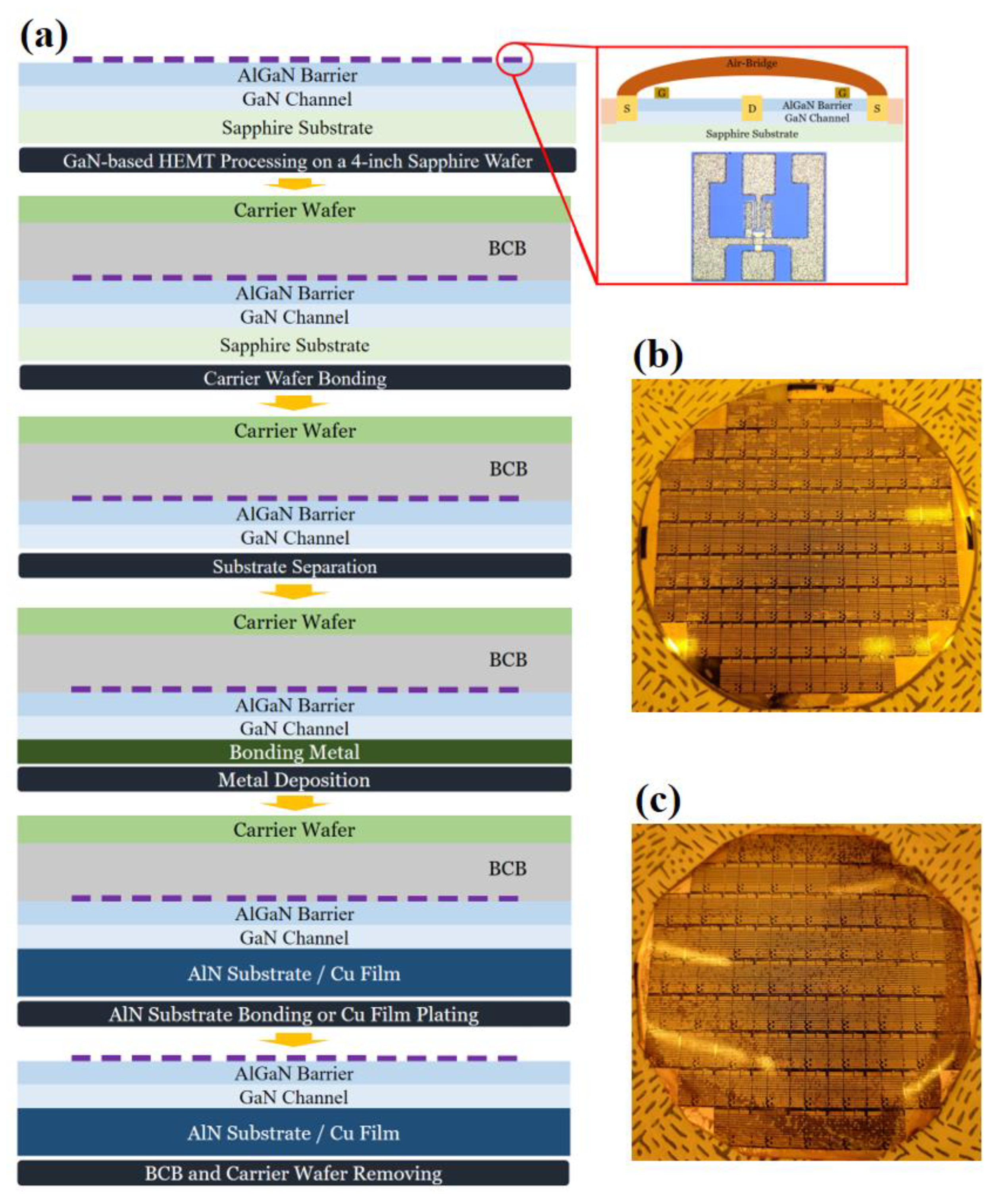
2. Device Fabrication

GaN-based HEMTs were processed on c-plane 4-inch sapphire substrates. The epitaxial layers, which were grown by a metal-organic chemical vapor deposition, were composed of a GaN channel (3.5 µm), AlN interfacial layer (1 nm), and Al0.26Ga0.74N barrier (25 nm) layers from the bottom to the top. To form the Ohmic contact, Ti/Al/Ni/Au (=30/100/30/100 nm) were deposited via an e-beam evaporator system followed by rapid thermal annealing for 40 s at 850 °C. Phosphorus was implanted for the device isolation. A 20 nm-thick SiN was deposited by a chemical vapor deposition system to passivate the devices. To open the contact pads, the SiN passivation layer was etched by inductively coupled plasma (ICP) etching. The SiN etching was conducted with CF4 gas for the gas flow of 30 sccm, RF power of 50 W, and process pressure of 10 mTorr. Ti/Au (=30/370 nm) was deposited by the e-beam evaporator system to form the contact pads. To define the gate electrode area, the SiN passivation layer was etched by the ICP etching system. Ni/Au (=30/100 nm) was deposited by the e-beam evaporator system to form the gate electrodes. A 3 µm-thick Au was plated to interconnect the distance source electrodes. The geometries of the processed GaN-based HEMTs were 1, 0.5, 3.5, and 200 µm for source-to-gate distance (LSG), gate length (LG), gate-to-drain distance (LGD), and total gate width (WG), respectively. The number of gate fingers (NF) is two.
To separate AlGaN/GaN film including the processed GaN-based HEMTs from the original substrate, the front-side of the sapphire substrate was bonded to a carrier wafer by using benzocyclobutene (BCB). The back-side of the sapphire substrate was thinned to 100 µm and polished to penetrate the ultraviolet-ray. The AlGaN/GaN film split at the GaN/sapphire interface when the ultraviolet-ray radiated from the back-side of the sapphire substrate. For AlN substrate bonding and Cu plating, Ti/Ni/Ti/Ni/Cu/Ni/Sn/Au (=200/200/200/200/2000/800/2000/5 nm) and Ti/Cu (=100/500 nm) were deposited at the back-side of AlGaN/GaN film, respectively. The bonding metal system was designed for the consideration of the wafer bowing, bonding metal intermixing, and compensating for the pressure and temperature deviation that was generated during the wafer bonding and plating process. After AlN substrate bonding or 100 µm-thick Cu plating, the carrier wafer and BCB were removed. Figure 1 shows the back-side process flow for the device transfer from sapphire substrate onto AlN substrate or Cu film which includes LLO and metal bonding process. Several back-side processing conditions including Cu plating and BCB removing should be further optimized.

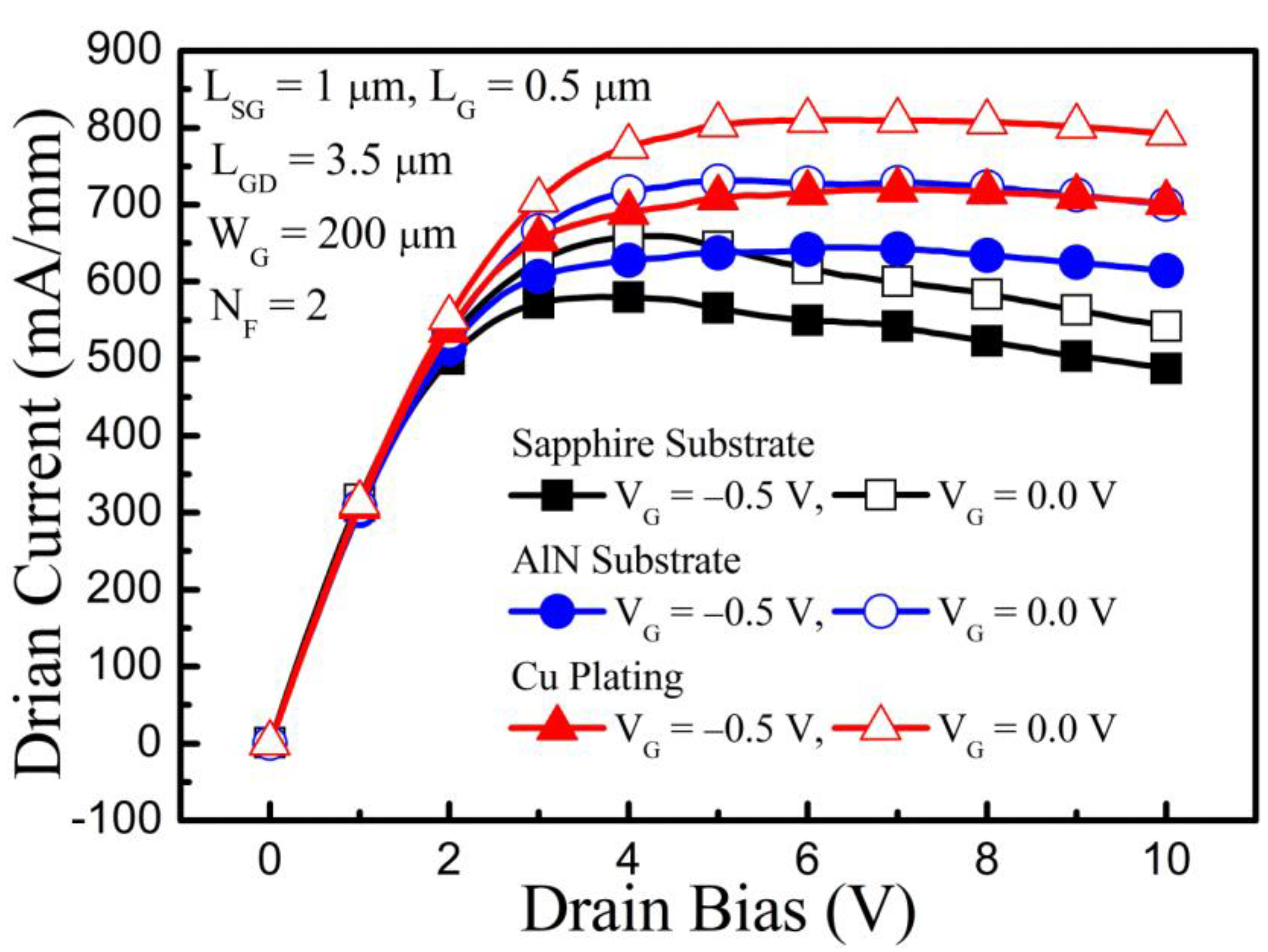
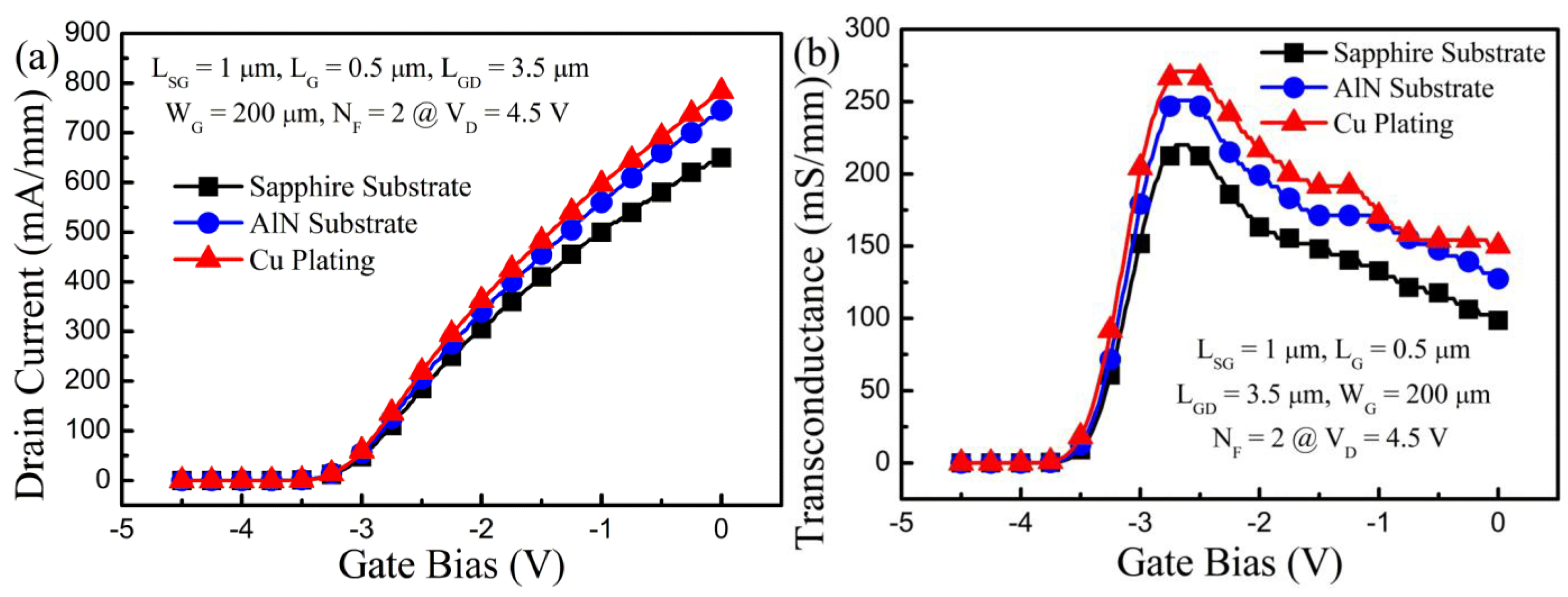
3. Results and Discussion

In Figure 2, the output characteristics of GaN-based HEMTs were measured to verify the substrate effects on the self-heating effect. The ID was enlarged with the increased thermal conductivity of the substrate/film. When the device operated on the sapphire substrate, the ID showed a maximum value at VD ≈ 4.0 V. Then, the ID decreased with increasing VD due to the self-heating effect [14,24], which limits the output power of GaN-based HEMTs. However, when the devices were operated on AlN substrate or Cu film, the ID was increased and a negligible ID reduction was observed. The 18% and 47% improvement of ID at VD = 4.0 V and VD = 10 V, respectively, was obtained with Cu film, compared to sapphire substrate. This result reflects the lesser degree of self-heating effect in GaN-based HEMTs which are operated on a higher thermal conductivity substrate/film than sapphire substrate [14].
We investigated the typical transfer properties for various substrates/films as shown in Figure 3. As we expected from Figure 2, the ID increased when the device was operated on AlN substrate or Cu film. The gm increases as well. The gm maximum increased by 14% and 23% with AlN substrate and Cu film, respectively, as compared to the sapphire substrate.
In order to figure out the clue of ID and gm improvement with AlN substrate and Cu film, the µ under the gated region was extracted for various substrates/films (Figure 4). Unlike the Si-based conventional metal-oxide-semiconductor device, the contact and access region (i.e., the source-to-gate and gate-to-drain regions) resistances should be considered to achieve the precise µ behavior, since the effective drain bias that was applied under the gated region is less than the applied bias at the drain electrode.
To extract the precise µ behavior under the gated region,
µ = [(ID/VD_Effective]LG]/(qWGNS)
was used [25,26], where q is the electron charge; Ns is the electron concentration located at AlGaN/GaN hetero-interface, which is estimated by integrating the C(V) curve; and VD_Effective is the effective drain bias that was induced under the gated region, as shown in
VD_Effective = VDID(RACC + 2RC)
RC and RACC are the contact and access region resistances, respectively, which are obtained by using the transmission line method (TLM).
At a low carrier density regime (<1.5 × 1012 cm−2), the µ curves were identical for the three different substrates/films. However, the maximum µ improved with the increased thermal conductivity of the substrate/film. The maximum µ was enhanced by 13% for the Cu film compared to the sapphire substrate. This phenomenon reflects how the DC characteristics and µ improvement are due to the reduced optic phonon scattering [26] and diminished self-heating effect.
Before and after the back-side processing, we compared the sheet resistance at the access region through the TLM. The sheet resistance improved (sapphire substrate: 408 Ω/sq.; AlN substrate: 393 Ω/sq.; Cu film: 389 Ω/sq.) with AlN substrate and Cu film. But, the sheet resistance reduction was relatively small, 3.7% and 4.7% for AlN substrate and Cu film, respectively, compared to a DC property that required further investigation. One possible scenario is that the access region temperature, when operating the devices is not as high as the temperature at the gate region and gate edge [8]. Therefore, the impact of the substrate on the sheet resistance at the access region is not as great as the gated region and DC properties.
The contact resistance extracted from the TLM did not change after the back-side processing. The extracted contact resistance values were 2.65, 2.62, and 2.66 Ω for sapphire substrate, AlN substrate, and Cu film, respectively. The back-side processing did not introduce contact resistance deterioration.
In Figure 5, the C(V) measurements were conducted before and after the back-side processing to investigate the 2-dimensional electron gas (2DEG) density variation that resulted from the back-side processing. The lateral shift of the C(V) curve after the back-side processing was negligible. The capacitance curves at −2.5 V ≤ VG ≤ 0 V were identical for various substrates/films. Therefore, the 2DEG density achieved by integrating the C(V) curve did not vary after the back-side processing.
Defect generation was also studied through the frequency dispersion since the defects located close to AlGaN/GaN hetero-interface degrade the device performance and long-term reliability. When the C(V) curves were measured for AlN substrate and Cu film, the C(V) curves at 10 kHz and 1 MHz overlapped as they were before the back-side processing. These results reflect that any significant defects near the GaN channel were net generated by the back-side processing.
In Figure 6, the pulse-mode stress measurements were conducted to verify the defects that were generated during the back-side process, which degrade the device performance. When the pulse-mode stress is introduced, the charges are trapped in GaN-based HEMTs. The trapped charges close to AlGaN/GaN hetero-interface modify the carrier density and drain current of the device [27]. For the pulse-mode stress measurement, a pulse applied at the drain electrode increased from 0 V to 10 V, whereas the pulse applied at the gate electrode was fixed at −2 V. In the pulse-mode stress measurements, (VG = 0 V, VD = 0 V) and (VG = −6 V, VD = 10 V) were presented at the quiescent biases for the without- and with-stress conditions, respectively. The applied pulse width of 0.2 µsec was separated by 1 msec.
For the three samples, ID was reduced, when the pulse-mode stress was provided, compared to the without-stress condition. However, the amount of ID reduction was not increased after the back-side processing, which shows that the critical defects close to AlGaN/GaN hetero-interface were not caused by the back-side processing.
The RF characteristics were also investigated for various substrates/films in Figure 7. For the RF property characterization, we first measured the S-parameter through the network analyzer. To extract the fT, the measured S-parameter was converted to the H-parameter. Then, a linear line with a −20 dB slope was fit on the H21 curve. The extrapolated point of the −20 dB slope linear line to the 0 dB is determined as fT. For the fMAX extraction, the measured S-parameter was converted to the maximum stable gain/maximum available gain. The −20 dB slope linear line was fit the stability factor (K) = 1. The extrapolated point of the linear line to 0 dB should be fMAX.
Compared to the sapphire substrate, the fT increased from 14.8 to 16.3 and 16.6 GHz with AlN substrate and Cu film, respectively. The fMAX was obtained 28.6 GHz for the sapphire substrate. After the back-side processing, the fMAX improved to 31.1 and 32.6 GHz for AlN substrate and Cu film, respectively. The improved RF property was relatively less than that of the DC property since the parasitic capacitance increased by the absence of the dielectric substrate.
Note that except for edge of the 4-inch wafer, we obtained the very similar DC and RF measurement results before and after the back-side processing. The electrical properties of GaN-based HEMTs for various substrates/films were summarized in Table 1, which were obtained at the middle of the processed wafer.

4. Conclusions

To investigate the substrate effect on the electrical properties in GaN-based HEMTs, AlGaN/GaN film including processed GaN-based HEMTs were separated from the sapphire substrate via the LLO technique and transferred onto the AlN substrate or plated 100 µm-thick Cu film at the back-side of devices. When GaN-based HEMTs were operated on AlN substrate and Cu film, they acted as the heat spreader. The DC and RF properties in terms of the drain current, transconductance, cut-off frequency, and maximum oscillation frequency were improved with increasing the thermal conductivity of the substrates/films since the self-heating effect was diminished, carrier mobility under the gated region was increased, and sheet resistance at the access region was ameliorated. The C(V) and pulse-mode stress measurements have revealed that there was no significant defect generation located close to AlGaN/GaN hetero-interface and the 2DEG density did not vary after the back-side processing. Our approach should be further investigated and optimized for the device transfer onto a higher thermal conductivity substrate such as diamond substrate without losing its original substrate.

Author Contributions

Conceptualization, S.-J.C., S.-B.B., H.-H.J. and J.-W.L.; methodology, S.-J.C., K.-J.C., S.-Y.L., J.-H.L., H.-W.J. and H.-C.K.; validation, S.-J.C.; formal analysis, S.-J.C. and I.-G.C.; investigation, S.-J.C.; writing—original draft preparation, S.-J.C.; writing—review and editing, S.-J.C. and H.-C.K.; project administration, H.-K.A.; funding acquisition, H.-K.A. All authors have read and agreed to the published version of the manuscript.

Funding

This research was supported by the Civil-Military Technology Cooperation Program (No. 19-CM-BD-05).

Conflicts of Interest

The authors declare no conflict of interest.

References

  1. Kummer, V.; Lu, W.; Schwindt, R.; Kuliev, A.; Simin, G.; Yang, J.; Khan, M.A.; Adesida, I. AlGaN/GaN HEMTs on SiC with fT of over 120 GHz. IEEE Electron. Device Lett. 2002, 23, 455–457. [Google Scholar] [CrossRef]
  2. Palacios, T.; Chakraborty, A.; Rajan, S.; Poblenz, C.; Keller, S.; DenBaars, S.P.; Speck, J.S.; Mishra, U.K. High-power AlGaN/GaN HEMTs for Ka-band applications. IEEE Electron. Device Lett. 2005, 26, 781–783. [Google Scholar] [CrossRef] [Green Version]
  3. Ahn, S.; Kim, B.-J.; Lin, Y.-H.; Ren, F.; Pearton, S.J.; Yang, G.; Kim, J.; Kravchenoko, I.I. Effect of proton irradiation dose on InAlN/GaN metal-oxide semiconductor high electron mobility transistors with Al2O3 gate oxide. J. Vac. Sci. Technol. B 2016, 34, 051202. [Google Scholar] [CrossRef]
  4. Gao, Z.; Romero, M.F.; Redondo-Cubero, A.; Pampillon, M.A.; Andres, E.S.; Calle, F. Effect of Gd2O3 gate dielectric on Proton-Irradiated AlGaN/GaN HEMTs. IEEE Electron. Device Lett. 2017, 38, 611–614. [Google Scholar] [CrossRef]
  5. Chang, S.-J.; Kim, D.-S.; Kim, T.-W.; Lee, J.-H.; Bae, Y.; Jung, H.-W.; Kang, S.C.; Kim, H.; Noh, Y.-S.; Lee, S.-H.; et al. Comprehensive research of total ionizing dose effects in GaN-based MIS-HEMTs using extremely thin gate dielectric layer. Nanomaterials 2020, 10, 2175. [Google Scholar] [CrossRef]
  6. Chang, S.-J.; Cho, K.J.; Jung, H.-W.; Kim, J.-J.; Jang, Y.-J.; Bae, S.-B.; Kim, D.-S.; Bae, Y.; Yoon, H.S.; Ahn, H.-K.; et al. Improvement of proton radiation hardness using ALD-deposited Al2O3 gate insulator in GaN-based MIS-HEMTs. ECS J. Solid State Sci. Technol. 2019, 8, Q245–Q248. [Google Scholar] [CrossRef]
  7. Adesida, I.; Lu, W.; Kummar, V. AlGaN/GaN HFETs for low noise applications. In Proceedings of the 6th International Conference on Solid-State and Integrated Circuit Technology, Shanghai, China, 6 August 2001; pp. 1163–1168. [Google Scholar]
  8. Zhao, M.; Liu, X.; Zheng, Y.; Peng, M.; Ouyang, S.; Li, Y.; Wei, K. Thermal analysis of AlGaN/GaN high-electron-mobility transistors by infrared microscopy. Opt. Commun. 2013, 291, 104–109. [Google Scholar] [CrossRef]
  9. Karmalkar, S.; Mishra, U.K. Enhancement of breakdown voltage in AlGaN/GaN high electron mobility transistors using a filed plate. IEEE Trans. Electron. Devices 2001, 48, 1515–1521. [Google Scholar] [CrossRef]
  10. Kuzmik, J.; Javorka, R.; Alam, A.; Marso, M.; Jeuken, M.; Cordos, P. Determination of channel temperature in AlGaN/GaN HEMTs grown on sapphire and silicon substrate using DC characterization method. IEEE Trans. Electron. Devices 2002, 49, 1496–1498. [Google Scholar] [CrossRef]
  11. Arulkumaran, K.R.S.; Ng, G.I.; Sandupatra, A. Investigation of self-heating effect on DC and RF performances in AlGaN/GaN HEMTs on CVD-diamond. J. Electron. Devices Society 2019, 7, 1264–1269. [Google Scholar]
  12. Kuball, M.; Pomeroy, J.W.; Simms, R.; Riedel, G.J.; Ji, H.; Sarua, A.; Uren, M.J.; Martin, T. Thermal Properties and reliability of GaN microelectronics: Sub-micron spatial and nanosecond time resolution thermography. In Proceedings of the IEEE Compound Semiconductor Integrated Circuit Symposium, Portland, OR, USA, 14–17 October 2007; pp. 1–4. [Google Scholar]
  13. Hu, H.; Tang, B.; Wan, H.; Sun, H.; Zhou, S.; Dai, J.; Chen, C.; Liu, S.; Guo, L.J. Boosted ultraviolet electroluminescence of InGaN/AlGaN quantum structures grown on high-index contrast patterned sapphire with silica array. Nano Energy 2020, 69, 104427. [Google Scholar] [CrossRef]
  14. Ji, H.; Das, J.; Germain, M.; Kuball, M. Laser lift-off transfer of AlGaN/GaN HEMTs from sapphire onto Si: A thermal perspective. Solid-State Electron. 2009, 53, 526–529. [Google Scholar] [CrossRef]
  15. Liu, T.; Kong, Y.; Wu, L.; Guo, H.; Zhou, J.; Kong, C.; Chen, T. Chen 3-inch GaN-on-Diamond HEMTs with device-first transfer technology. IEEE Electron. Device Lett. 2017, 38, 1417–1420. [Google Scholar] [CrossRef]
  16. Hirama, K.; Taniyasu, Y.; Kasu, M. AlGaN/GaN high-electron mobility transistors with low thermal resistance grown on single-crystal diamond (111) substrates by metalorganic vapor-phase epitaxy. Appl. Phys. Lett. 2011, 98, 162112. [Google Scholar] [CrossRef]
  17. Gerrer, T.; Czap, H.; Maier, T.; Benkjelifa, F.; Muller, S.; Nobel, C.E.; Waltereit, P.; Quay, R.; Cimalla, V. 3 GHz RF measurements of AlGaN/GaN transistors transferred from silicon substrate onto single crystalline diamond. AIP Adv. 2019, 9, 125106. [Google Scholar] [CrossRef] [Green Version]
  18. Wong, W.S.; Sands, T.; Cheung, N.W.; Kneissl, M.; Bour, D.P.; Mei, P.; Romano, L.T.; Johnson, N.M. Fabrication of thin-film InGaN light-emitting diode membranes by laser lift-off. Appl. Phys. Lett. 1999, 75, 1360. [Google Scholar] [CrossRef]
  19. Wierer, J.J.; Steigerwald, D.A.; Krames, M.R.; O’shea, J.J.; Ludowise, M.J.; Christenson, G.; Shen, Y.-C.; Lowery, C.; Martin, P.S.; Subramanya, S.; et al. High power AlGaLiN filp-chip light-emitting diodes. Appl. Phys. Lett. 2001, 78, 3379. [Google Scholar] [CrossRef]
  20. Bao, K.; Kang, X.N.; Zhang, B.; Dai, T.; Sun, Y.J.; Fu, Q.; Lian, C.J.; Xiong, G.C.; Zhang, G.Y.; Chen, Y. Improvement of light extraction from GaN-based thin-film light-emitting diodes by patterning undoped GaN using modified laser lift-off. Appl. Phys. Lett. 2007, 92, 141104. [Google Scholar] [CrossRef]
  21. Lei, Y.; Wan, H.; Tang, B.; Lan, S.; Miao, J.; Wan, Z.; Liu, Y.; Zhou, S. Optical characterization of GaN-based vertical blue light-emitting diodes on p-type silicon substrate. Crystals 2020, 10, 621. [Google Scholar] [CrossRef]
  22. Zhao, M.; Tang, X.; Huo, W.; Han, L.; Deng, Z.; Jiang, Y.; Wang, W.; Chen, H.; Du, C.; Jia, H. Characteristics of AlGaN/GaN high electron mobility transistors on metallic substrate. Chin. Phys. B 2020, 29, 048104. [Google Scholar] [CrossRef]
  23. Wang, X.; Lo, C.-F.; Liu, L.; Cuervo, C.V.; Fan, R.; Pearton, S.J.; Bila, B.; Johns, M.R.; Zhou, L.; Smith, D.J.; et al. 193 nm excimer laser lift-off for AlGaN/GaN high electron mobility transistors. J. Vac. Sci. Technol. B 2012, 30, 061209. [Google Scholar] [CrossRef]
  24. Nigam, A.; Bhat, T.N.; Rajamani, S.; Dolmanan, S.B.; Tripathy, S.; Kumar, M. Effect of self-heating on electrical characteristics of AlGaN/GaN HEMT on (111) substrate. AIP Adv. 2017, 7, 085015. [Google Scholar] [CrossRef]
  25. Chang, S.-J.; Jung, H.-W.; Do, J.-W.; Cho, K.J.; Kim, J.-J.; Jang, Y.J.; Yoon, H.S.; Ahn, H.-K.; Min, B.-G.; Kim, H.; et al. Enhanced carrier transport properties in GaN-based metal-insulator semiconductor high electron mobility transistor with SiN/Al2O3 bi-layer passivation. ECS J. Solid State Sci. Technol. 2018, 7, N86–N89. [Google Scholar] [CrossRef]
  26. Chang, S.-J.; Kang, H.-S.; Lee, J.-H.; Yang, J.; Bhuiyan, M.; Jo, Y.-W.; Cui, S.; Lee, J.-H.; Ma, T.-P. Investigation of channel mobility in AlGaN/GaN high electron-mobility transistors. Jpn. J. Appl. Phys. 2016, 55, 044104. [Google Scholar] [CrossRef]
  27. Lee, J.-H.; Kim, J.-G.; Ju, J.-M.; Ahn, W.-H.; Kang, S.-H.; Lee, J.-H. AlInGaN/GaN double-channel FinFET with high on-current and negligible current collapse. Solid State Electron. 2020, 164, 107678. [Google Scholar] [CrossRef]
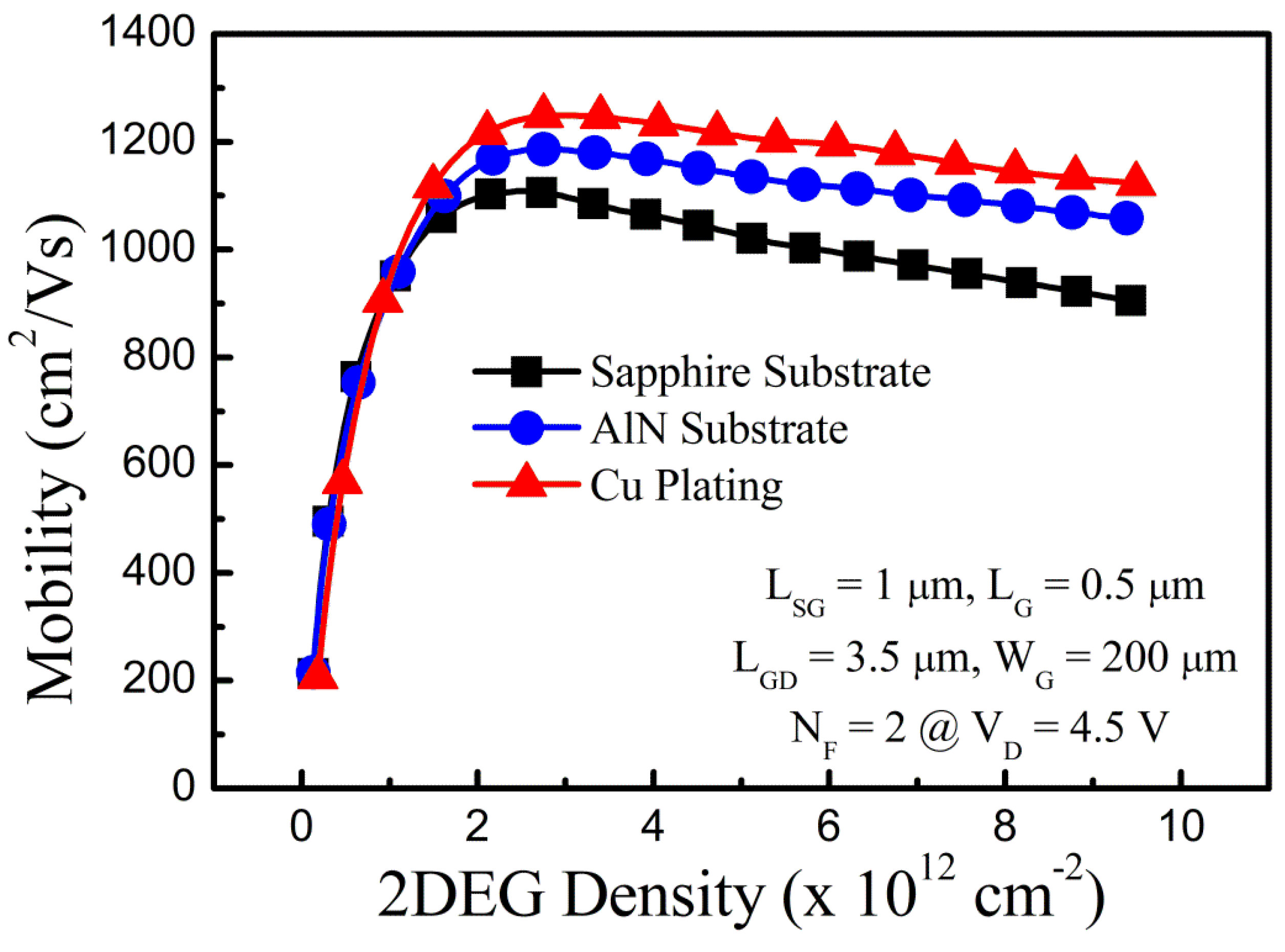
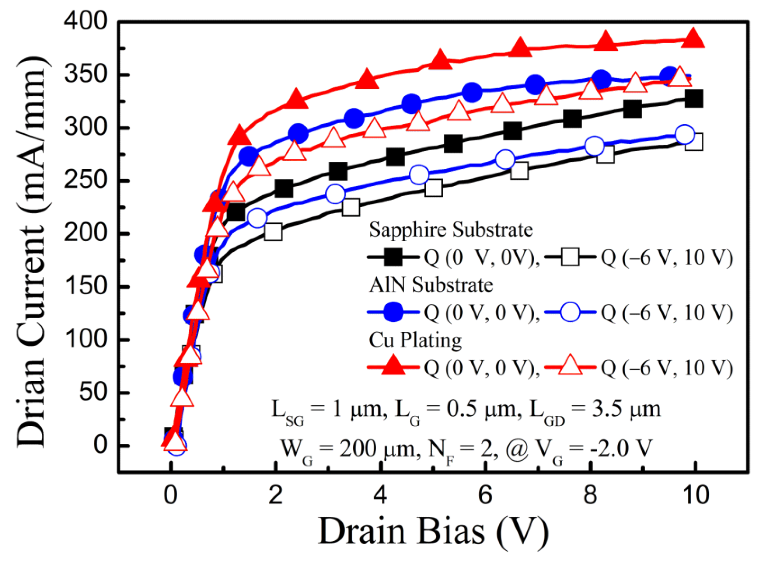
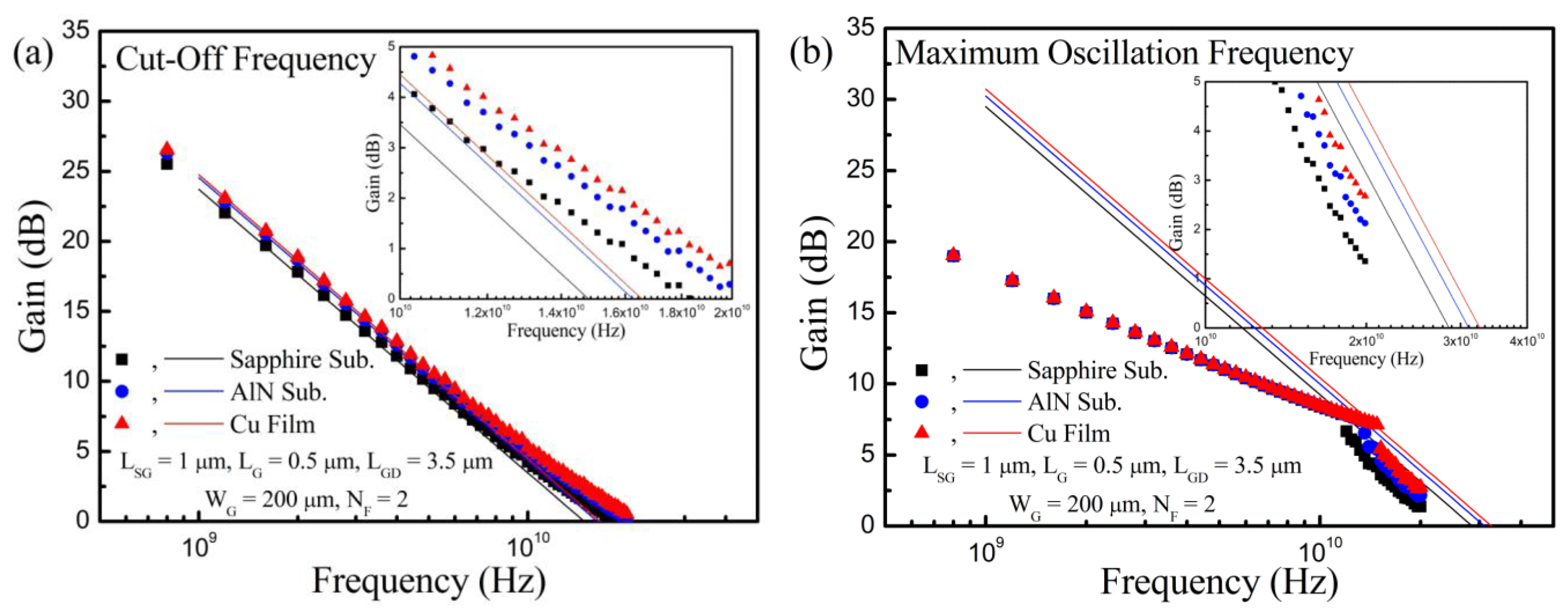
Figure 1. (a) Back-side process flow for the 4-inch wafer scale AlGaN/GaN film transference onto AlN substrate or Cu film. Zoomed-in images show the cross-section view and microscope image of the processed GaN-based HEMT. Processed wafers (b) bonded to AlN substrate and (c) plated Cu film.
Crystals 11 01414 g001
Figure 2. Output characteristics of GaN-based HEMTs operated on sapphire substrate, AlN substrate and Cu film. Drain current vs. Drain bias.
Crystals 11 01414 g002
Figure 3. Transfer characteristics of GaN-based HEMTs operated on sapphire substrate, AlN substrate, and Cu film. (a) Drain current and (b) transconductance as a function of gate bias.
Crystals 11 01414 g003
Figure 4. Extracted carrier mobility under the gated region in GaN-based HEMTs operated on sapphire substrate, AlN substrate, and Cu film. Carrier mobility as a function of 2DEG density.
Crystals 11 01414 g004
Figure 5. C(V) measurement results. Capacitance vs. gate bias at 10 kHz and 1 MHz for sapphire substrate, AlN substrate, and Cu film. Inset shows the zoomed-in C(V) curves at −3.5 V ≤ VG ≤ −2.5 V.
Crystals 11 01414 g005
Figure 6. Pulse-mode stress measurement results in GaN-based HEMTs operated on sapphire substrate, AlN substrate, and Cu film with the quiescent bias of (0 V, 0 V) and (−6 V, 10 V).
Crystals 11 01414 g006
Figure 7. RF characteristics measured in GaN-based HEMTs operated on sapphire substrate, AlN substrate, and Cu film. (a) Cut-off frequency and (b) maximum oscillation frequency characteristics before and after the back-side processing.
Crystals 11 01414 g007
Table 1. Summarized GaN-based HEMTs properties corresponding to the substrates/films in this paper.
ParameterID at VG = 0.0 V
(mA/mm)
gm,max (mS/mm)Max. µ
(cm2/Vs)
RSH
(Ω/sq)
fT
(GHz)
fMAX
(GHz)
at VD = 4.0 Vat VD = 10.0 V
Sapphire Substrate658542220110940814.828.6
AlN Substrate717705251118939316.331.1
Cu Film776795271125338916.632.6
Publisher’s Note: MDPI stays neutral with regard to jurisdictional claims in published maps and institutional affiliations.

