
Surface-Passivated CsPbBr3 for Developing Efficient and Stable Perovskite Photovoltaics

1
Department of Energy and Materials Engineering and Research Center for Photoenergy Harvesting & Conversion Technology (PHCT), Dongguk University, Seoul 04620, Korea
2
Green and Sustainable Materials R&D Department, Korea Institute of Industrial Technology (KITECH), Cheonan-si 31056, Korea
*
Authors to whom correspondence should be addressed.
†
Theses authors contributed equally to this work.
Crystals 2021, 11(12), 1588; https://0-doi-org.brum.beds.ac.uk/10.3390/cryst11121588
Submission received: 6 December 2021
/
Revised: 14 December 2021
/
Accepted: 17 December 2021
/
Published: 20 December 2021
(This article belongs to the Special Issue Advance in Application of Perovskite Materials in Optoelectronic Devices)
Abstract
:All-inorganic perovskites consisting of only inorganic elements have been recently considered as highly stable semiconductors for photoactive layer of optoelectronics applications. However, the formation of high-quality thin film and trap-reduced interface has still remains an important task, which should be solved for improving the performances of all-inorganic perovskite-based photovoltaics. Here, we adopted facile method that could reduce charge-carrier recombination by depositing a passivation agent on the top surface of the CsPbBr3 all-inorganic perovskite layer. We also found that the CsPbBr3 perovskite photovoltaic prepared from surface treatment method using n-octylammonium bromide provides an improved stability in ambient environment and 1-sun illuminating condition. Therefore, the perovskite photovoltaics fabricated from our approach offered an improved power conversion efficiency of 5.44% over that of the control device without surface treatment (4.12%).
1. Introduction
Perovskite photovoltaics (PPVs) have been enormously explored as next-generation energy harvesting devices during the last decades. Their power conversion efficiencies (PCEs) have been reported to be over 25% [1], which is competitive with the efficiencies of conventional silicon photovoltaics. Hence, investigations on module fabrication [2], device encapsulation [3] and cost-effective production [4] of materials have been initiated in order to realize large-scale manufacturing as well as a highly stable operation under light illumination, which are required for the commercialization of PPVs.
All-inorganic perovskites have recently emerged as considerable approaches for achieving long-term stable PPVs. They have been developed by introducing inorganic cation instead of thermally decomposable organic cations that cause the limited stabilities in organic–inorganic hybrid perovskites and thus have possibly provided a significantly retarded degradation at the elevated temperature generated by light exposure during device operation [5]. Therefore, several studies on perovskite component [6], film fabrication [7] and device structure have been continuously attempted so far for improving the qualities of all-inorganic perovskites and the performances of its corresponding PPVs.
However, the efficiencies of PPVs fabricated by employing all-inorganic perovskites as photo-active layer materials have not still reached those of devices fabricated with organic-inorganic perovskites. One of suggested reasons for these limited efficiencies in the all-inorganic PPVs is the high density of interfacial traps [8], inducing large loss of photocurrent through recombination of charge-carriers [9]. Particularly, CsPbBr3, which has been regarded as a promising wide bandgap photo-absorber with exceptional stability, and its corresponding PPVs have shown efficiencies up to 11.08% [10,11]. Moreover, CsPbBr3 PPVs have been typically investigated by adapting the device structure with the direct junction between perovskite layer and carbon electrode [12], and as a result, these PPVs have still afforded the inadequate contact accompanied by insufficient interfacial interaction, leading to large open-circuit voltage (VOC) deficit of ~0.6 eV [13].
Here, we report efficient and stable all-inorganic CsPbBr3 PPVs by incorporating surface treatment using n-octylammonium bromide (OABr) [14,15,16,17]. It was observed that the CsPbBr3 PPV with surface treatment provides a higher PCE of 5.44% compared with the control device without treatment (PCE = 4.12%). Then, the enhanced performance of CsPbBr3 PPV after surface treatment was investigated using light-intensity dependent photovoltaic performances, photoluminescence (PL) measurements, and trap density analysis. From the systematic analysis, we revealed that the trap density of CsPbBr3 PPV is reduced after surface treatment using OABr, leading to the facilitated charge transfer and extraction at perovskite/top electrode interface in PPV. Therefore, it could be demonstrated that surface treatment is an efficient strategy for improving device performances of all-inorganic CsPbBr3 PPVs.
2. Materials and Methods
2.1. Materials
CsBr, PbBr2, 2-propanol (IPA), dimethyl sulfoxide (DMSO) and chloroform (CF) were procured from Sigma-Aldrich. OABr was purchased from Greatcell solar. Fluorine-doped tin oxide (FTO) on glass (7 Ω sq−1) was obtained from Asahi. Compact TiO2 (c-TiO2, SC-BT 060), mesoporous TiO2 (m-TiO2, SC-BT 040) were procured from ShareChem Co., Ltd. (Hwaseong, South Korea). Carbon electrode was purchased in Solaronix Co., Ltd. (Aubonne, Switzerland).
2.2. Photovoltaic Fabrication
Detergent, deionized water, and IPA were used to clean the FTO substrates. To form the c-TiO2 layer on the FTO substrates, the SC-BT 060 solution diluted in ethanol (1:2 v/v) was spin-coated at 3000 rpm for 30 s, followed by sintering at 450 °C for 30 min. The m-TiO2 layer was deposited by spinning the SC-BT 040 paste mixed with ethanol and IPA (1:1:4 v/v/v) at 3000 rpm for 30 s and then was sintered at 500 °C for 30 min. CsPbBr3 precursor solution was made by dissolving 110 mg of CsBr and 190 mg of PbBr2 in 1 mL of DMSO. The perovskite layer was spin-coated at 2000 rpm for 60 s from the precursor solution and then was annealed for 30 min at 150 °C. The surface treatment was performed by spin-coating of the OABr solution (15 mM in CF) and subsequent annealing at 100 °C for 5 min. Finally, the carbon electrode was formed by doctor-blade coating using carbon paste, followed by drying at 150 °C for 30 min.
2.3. Characterization
The morphologies of perovskite layers were studied using scanning electron microscope (SEM) (Hitachi S-3000N, Tokyo, Japan). UV–VIS absorption spectra was obtained using UV–VIS spectrophotometer (Scinco S-3100, Seoul, South Korea). The intensity of solar simulator (Xenon lamp, McScience, Seoul, South Korea) was calibrated by a standard mono-Si PV device (PVM-396, PV Measurements Inc., Boulder, CO, USA) certified by the National Renewable Energy Laboratory. Hysteresis index (HI) was calculated from the from the equation of (Pmax,rev − Pmax,fwd)/Pmax,rev. External quantum efficiency (EQE) spectra were measured via photo-modulation spectroscopy (McScience, K3100 Spectral IPCE Measurement System, Seoul, South Korea) under a monochromatic xenon light source with calibration using a Si photodiode certified by the National Institute for Standards and Technology. The J–V measurement under the simulated lights was performed from 1.4 V to −0.1 V with the scan rate of 150 mV s−1. Steady-state PL measurements were carried out with cary eclipse fluorescence spectrophotometer (Varian). Time-resolved PL measurements were recorded using a single photon counting system coupled with a single photon counting detector (wavelength of laser source for excitation = 435 nm) (FlouTime 300, PicoQuant, Berlin, Germany).
3. Results and Discussion
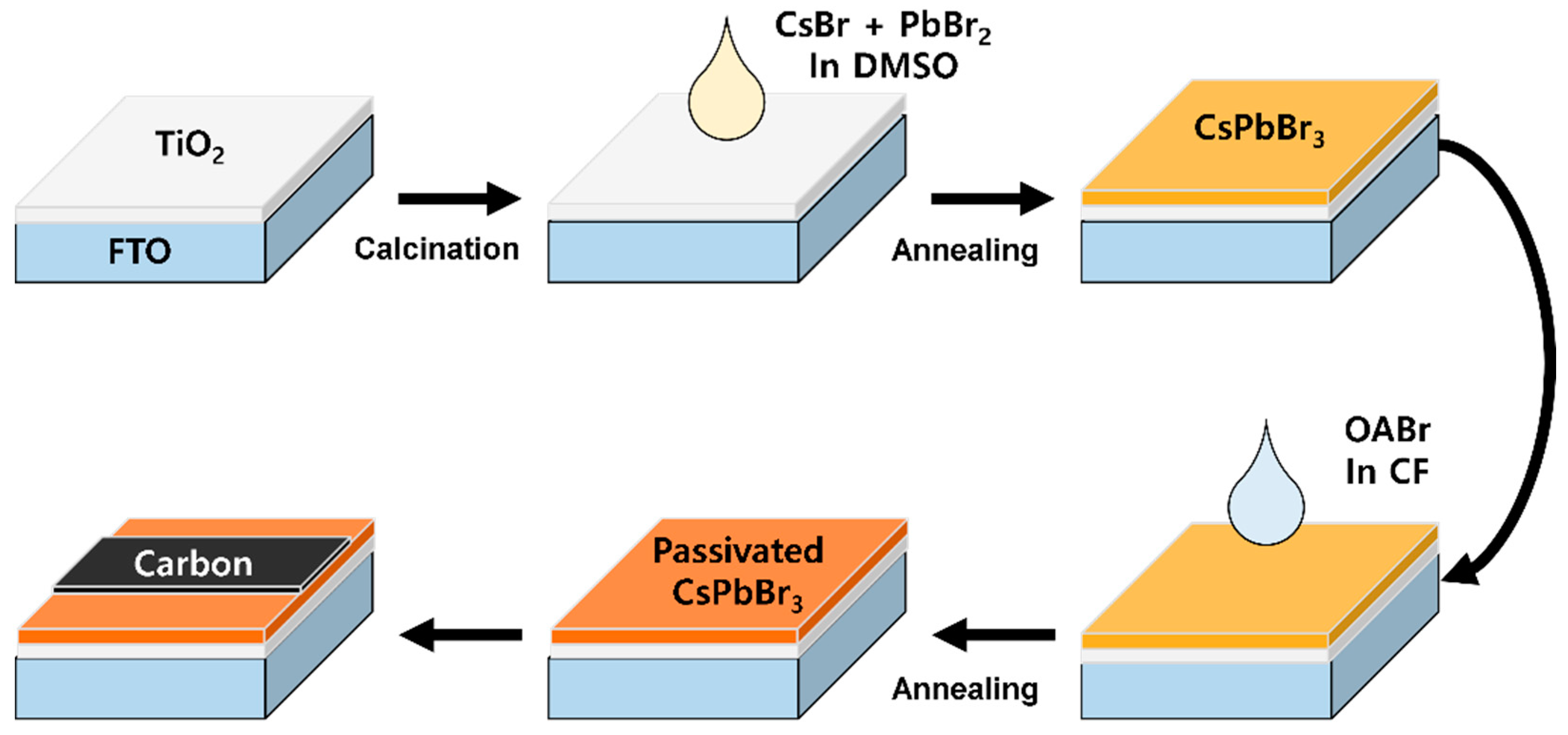
In this work, CsPbBr3 PPVs were fabricated with the device structure of FTO/TiO2/CsPbBr3/carbon electrode, as shown in Figure 1. The surface treatment of CsPbBr3 perovskite layer was performed by depositing OABr solution in CF on the top surface of CsPbBr3 layer and consecutive annealing process. No significant variation of morphologies of CsPbBr3 films before and after surface treatment were identified by measuring SEM (Figure S1). Thus, the morphological effects were excluded when comparing the device performances of PPVs with and without surface treatment [18,19].
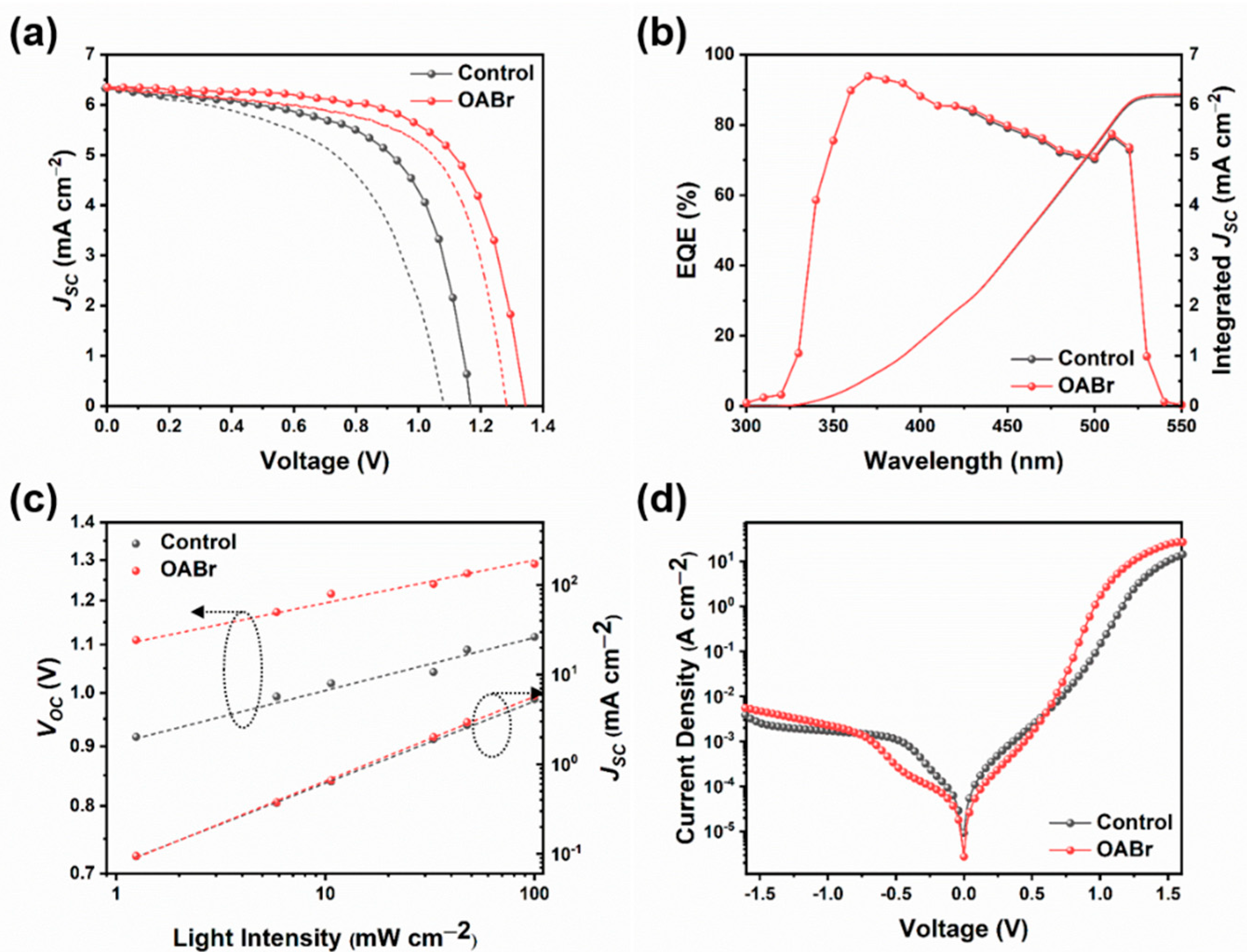
The effects of OABr surface treatment on the performances of CsPbBr3 PPVs were investigated by measuring J–V curves under AM 1.5 G illumination, as shown in Figure 2a and Table 1. Control CsPbBr3 PPV showed a PCE of 4.57% with an VOC of 1.17 V, a short-circuit current density (JSC) of 6.33 mA cm−2 and a fill factor (FF) of 61.7%. After introducing the surface treatment using OABr, the CsPbBr3 PPV provided an improved PCE of 5.63% with a VOC of 1.34 V, a JSC of 6.35 mA cm−2 and an FF of 66.2%. Then, the energy losses (Eloss) of CsPbBr3 PPVs were obtained from the difference between VOC from J–V characteristics and optical bandgap (2.31 eV) of CsPbBr3 from UV–Vis optical spectra [20]. The calculated Eloss values were 1.14 eV for the control device and 0.97 eV for the OABr-treated device. Since the OABr surface treatment did not lead to the shift of the absorbance edge of the CsPbBr3 films, as shown in Figure S2, the suppression of Eloss in OABr-treated PPV would imply that OABr surface treatment contributes to the reduced trap density. Additional possible reason for the reduced Eloss of PPVs after OABr treatment is the low dipole moment arising from the long alkyl chains, leading to the facilitated charge transfer at perovskite/carbon electrode interface in the PPV by inducing the better energy alignment [21,22,23,24,25].
Hysteresis index (HI) were also calculated through the comparison between J–V curves in forward and reverse scan [26]. Notably, the control device without treatment exhibited a large HI of 0.197, while the OABr-treated PPV provided a highly reduced HI of 0.0675 (Table S1). From these results, OABr surface treatment is suggested to be an effective approach for passivating wide band gap all-inorganic perovskites for PPV applications. The verification of current density was carried out using EQE measurement. The integrated JSC from EQE spectra were 6.18 and 6.22 mA cm−2 for control and OABr-treated devices, as shown in Figure 2b. The low differences (<10%) between JSC from J–V curve and EQE indicate that our photovoltaic measurements are done without critical error [27].
The enhanced performances of PPVs after introducing OABr surface treatment were further explored by measuring the light intensity-dependent photovoltaic parameters, as shown in Figure 2c [28]. The ideality (n) and the power factor (α) of PPVs were extracted using the below equations.
where q is the elementary charge, k is the Boltzmann constant, T is the absolute temperature, and Pin is the power density of input light. The n values for control and OABr-treated CsPbBr3 PPVs were 1.78 and 1.60, respectively. The α values were calculated to be 0.927 for control device and 0.947 for the OABr-treated device. The reduced n and the increased α of OABr-treated PPV compared with those of the control device indicate the efficient suppression of charge carrier recombination after introducing OABr surface treatment. This was also supported by J–V curves measured under dark condition, where the OABr-treated PPV afforded a lower dark current density than the control device, as shown in Figure 2d.
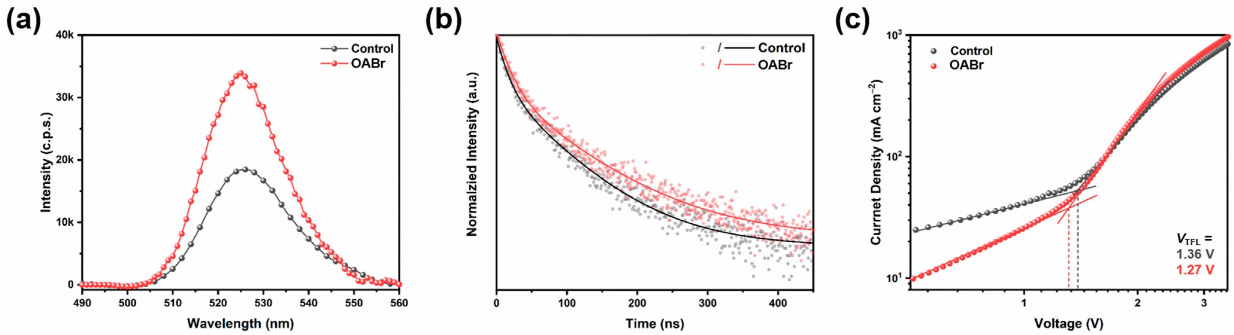
To gain deeper insight on the trap passivation of OABr on the CsPbBr3 films, steady-state and time-resolved PL analyses were carried out. As shown in Figure 3a, the increased intensity and blue shift were observed in the emission peak of steady-state PL spectra after the top surface of the CsPbBr3 film was treated with OABr [29]. The enhanced PL intensity referred to the suppression of non-radiative recombination [30], and the blue shift of PL peak possibly indicated the reduced trap density of the CsPbBr3 film by the interaction between CsPbBr3 and OABr after surface treatment [31].
Figure 3b shows the time-resolve PL spectra of CsPbBr3 films before and after OABr surface treatment. The data were fitted by using below bi-exponential equation.
The CsPbBr3 film after OABr surface treatment showed a prolonged PL lifetime of 247 ns compared with the control films (213 ns) (Table 2). The longevity of the charges on the surface would indicate higher chances of photo-generated charges being extracted from the photoactive layer to counter electrode [32]. The passivation of CsPbBr3 film after OABr surface treatment was further confirmed by fabricating the space charge limited current (SCLC) electron-only devices of FTO/TiO2/CsPbBr3/PCBM/Ag, as shown in Figure 3c. The trap densities of devices were calculated from the VTFL using the below equation.
L is the thickness of active layer (350 nm), q is the elementary charge, εr is the relative dielectric constant of the perovskite layer, ε0 is the vacuum permittivity, nt is the defect density. From the SCLC measurement, the defect densities were estimated to be 3.96 × 1016 cm−3 for the control device and 3.70 × 1016 cm−3 for the OABr-treated device. This reduced trap density after OABr surface treatment would result in the improved device performances of OABr-treated PPVs compared with the control device without treatment.
The long-term stabilities of CsPbBr3 PPVs were tested under ambient condition (~30 °C temperature and 25~35% relative humidity) without any encapsulation. As shown in Figure 4a, the control CsPbBr3 PPV without surface treatment showed a faster decay of photovoltaic performance and provided 80% of its initial PCE after storage test. However, the OABr-treated PPV showed an enhanced shelf-lifetime and retained 90% of its original PCE after 30 days of storage. The lengthened storage lifetime of the OABr-treated PPV would have originated from the hydrophobicity of long alky-chains from OABr [33] and reduced interfacial traps in PPVs. Additionally, maximum power point tracking of PPVs under 1-sun illumination were studied under a temperature of ~45 °C and constant bias of 1.0 V, as shown in Figure 4b. The OABr-treated CsPbBr3 PPVs preserved ~90% of initial power output after 18 h, while the control device showed ~70% of initial value. These stability results show the passivating CsPbBr3 films through OABr surface treatment is beneficial for preserving the device performance of PPVs.
4. Conclusions
In conclusion, we introduced the OABr surface treatment for improving photovoltaic performances of CsPbBr3 PPVs. The OABr-treated PPV showed a higher PCE of 5.44% as compared with the control device without treatment (4.12%), attributed to the efficient passivation of traps on the surface of CsPbBr3 layer after OABr surface treatment. The enhancement majorly resulted from a dramatic increased VOC from 1.17 V to 1.34 V. Furthermore, when stored in ambient or practical conditions, the OABr-treated PPV showed enhanced stabilities compared to the control device. This work demonstrates that the passivation of wide bandgap all-inorganic perovskites with OABr surface treatment could efficiently provide the practicality of all-inorganic PPVs for real-world applications.
Supplementary Materials
The following are available online at https://0-www-mdpi-com.brum.beds.ac.uk/article/10.3390/cryst11121588/s1. Figure S1: Top view SEM images of (a) control and (b) OABr-treated CsPbBr3 films, Figure S2: (a) UV–Vis spectra of CsPbBr3 films on glass substrates and (b) its corresponding Tauc plot, Figure S3: Detailed distribution data of (a)VOC, (b) JSC, (c) FF and (d) PCE for control and OABr-treated CsPbBr3 PPVs, Table S1: Photovoltaic parameters of CsPbBr3 PPVs with and without OABr surface treatment. Table S2: Photovoltaic parameters of reported CsPbBr3 PPVs.
Author Contributions
Conceptualization, J.W.J. and S.B.; methodology and investigation, H.J.T.; data curation, J.H.L.; writing—original draft preparation, H.J.T. and J.H.L.; writing—review and editing, J.W.J. and S.B.; supervision, J.W.J. and S.B. All authors have read and agreed to the published version of the manuscript.
Funding
This work was supported by the National Research Foundation of Korea (NRF) grant, funded by the Korea government (Ministry of Science and ICT, MSIT) (NRF-2019R1F1A1059791 and NRF-2020R1C1C101462412). This work was also conducted with the support of the Korea Institute of Industrial Technology as “Development of eco-friendly perovskite ink manufacturing technology for inkjet process of next-generation displays (KITECH EI-21-0015)”.
Data Availability Statement
Data are available on request from the authors.
Acknowledgments
H.T. and J.H.L. equally contributed to this work.
Conflicts of Interest
The authors declare no conflict of interest.
References
- Min, H.; Lee, D.Y.; Kim, J.; Kim, G.; Lee, K.S.; Kim, J.; Paik, M.J.; Kim, Y.K.; Kim, K.S.; Kim, M.G.; et al. Perovskite solar cells with atomically coherent interlayers on SnO2 electrodes. Nature 2021, 598, 444–450. [Google Scholar] [CrossRef] [PubMed]
- Bi, E.; Tang, W.; Chen, H.; Wang, Y.; Barbaud, J.; Wu, T.; Kong, W.; Tu, P.; Zhu, H.; Zeng, X.; et al. Efficient perovskite solar cell modules with high stability enabled by iodide diffusion barriers. Joule 2019, 3, 2748–2760. [Google Scholar] [CrossRef]
- Cheacharoen, R.; Rolston, N.; Harwood, D.; Bush, K.A.; Dauskardt, R.H.; McGehee, M.D. Design and understanding of encapsulated perovskite solar cells to withstand temperature cycling. Energy Environ. Sci. 2018, 11, 144–150. [Google Scholar] [CrossRef]
- Zhang, F.; Yao, Z.; Guo, Y.; Bergstrand, J.; Brett, C.J.; Cai, B.; Hajian, A.; Guo, Y.; Yang, X.; Gardner, J.M.; et al. Polymeric, Cost-Effective, Dopant-Free Hole Transport Materials for Efficient and Stable Perovskite Solar Cells. J. Am. Chem. Soc. 2019, 141, 19700–19707. [Google Scholar] [CrossRef]
- Liang, J.; Wang, C.; Wang, Y.; Xu, Z.; Lu, Z.; Ma, Y.; Zhu, H.; Hu, Y.; Xiao, C.; Yi, X.; et al. All-inorganic perovskite solar cells. J. Am. Chem. Soc. 2016, 138, 15829–15832. [Google Scholar] [CrossRef] [PubMed]
- Liang, J.; Zhao, P.; Wang, C.; Wang, Y.; Hu, Y.; Zhu, G.; Ma, L.; Liu, J.; Jin, Z. CsPb0.9Sn0.1IBr2 based all-inorganic perovskite solar cells with exceptional efficiency and stability. J. Am. Chem. Soc. 2017, 139, 14009–14012. [Google Scholar] [CrossRef]
- Wang, K.; Wang, R.; Wang, Z.; Li, M.; Zhang, Y.; Ma, H.; Liao, L.; Yang, Y. Tailored phase transformation of CsPbI2Br films by copper(II) bromide for high-performance all-inorganic perovskite solar cells. Nano Lett. 2019, 19, 5176–5184. [Google Scholar] [CrossRef]
- Yuan, J.; Zhang, L.; Bi, C.; Wang, M.; Tian, J. Surface trap states passivation for high-performance inorganic perovskite solar cells. Sol. RRL. 2018, 2, 1800188. [Google Scholar] [CrossRef]
- Wang, J.; Zhang, J.; Zhou, Y.; Liu, H.; Xue, Q.; Li, X.; Chueh, C.; Yip, H.; Zhu, Z.; Jen, A.K.Y. Highly efficient all-inorganic perovskite solar cells with suppressed non-radiative recombination by a Lewis base. Nat. Commun. 2020, 11, 177. [Google Scholar] [CrossRef]
- Zhou, Q.; Duan, J.; Du, J.; Guo, Q.; Zhang, Q.; Yang, X.; Duan, Y.; Tnag, Q. Tailored lattice “Tape” to confine tensile interface for 11.08%-efficiency all-inorganic CsPbBr3 perovskite solar cell with an ultrahigh voltage of 1.702 V. Adv. Sci. 2021, 8, 2101418. [Google Scholar] [CrossRef]
- Jeong, M.; Choi, I.W.; Go, E.M.; Cho, Y.; Kim, M.; Lee, B.; Jeong, S.; Jo, Y.; Choi, H.W.; Lee, J.; et al. Stable perovskite solar cells with efficiency exceeding 24.8% and 0.3-V voltage loss. Science 2020, 369, 1615–1620. [Google Scholar] [CrossRef]
- Duan, J.; Hu, T.; Zhao, Y.; He, B.; Tang, Q. Carbon-electrode-tailored all-inorganic perovskite solar cells to harvest solar and water-vapor energy. Angew. Chem. Int. Ed. 2018, 57, 5746–5749. [Google Scholar] [CrossRef]
- Liu, T.; Wang, Z.; Lou, L.; Xiao, S.; Zheng, S.; Yang, S. Interfacial post-treatment for enhancing the performance of printable carbon-based perovskite solar cells. Sol. RRL 2020, 4, 1900278. [Google Scholar] [CrossRef]
- Wang, R.; Tong, Y.; Manzi, A.; Wang, K.; Fu, Z.; Kentzinger, E.; Feldmann, J.; Urban, A.S.; Müller-Buschbaum, P.; Frielinghaus, H. preferential orientation of crystals induced by incorporation of organic ligands in mixed-dimensional hybrid perovskite films. Adv. Optical Mater. 2018, 6, 1701311. [Google Scholar] [CrossRef]
- Jiang, L.; Fang, Z.; Lou, H.; Lin, C.; Chen, Z.; Li, J.; He, H.; Ye, Z. Achieving long carrier lifetime and high optical gain in all inorganic CsPbBr3 perovskite films through top and bottom surface modification. Phys. Chem. Chem. Phys. 2019, 21, 21996–22001. [Google Scholar] [CrossRef] [PubMed]
- Hartono, N.T.P.; Thapa, J.; Tiihonen, A.; Oviedo, F.; Batali, C.; Yoo, J.J.; Liu, Z.; Li, R.; Marrón, D.F.; Bawendi, M.G.; et al. How machine learning can help select capping layers to suppress perovskite degradation. Nat. Commun. 2020, 11, 4172. [Google Scholar] [CrossRef] [PubMed]
- Yoo, J.J.; Wieghold, S.; Sponseller, M.C.; Chua, M.R.; Bertram, S.N.; Hartono, N.T.P.; Tresback, J.S.; Hansen, E.C.; Correa-Baena, J.-P.; Bulovic’, V. An interface stabilized perovskite solar cell with high stabilized efficiency and low voltage loss. Energy Environ. Sci. 2019, 12, 2192–2199. [Google Scholar] [CrossRef] [Green Version]
- Zheng, X.; Chen, B.; Dai, J.; Fang, Y.; Bai, Y.; Lin, Y.; Wei, H.; Zeng, X.C.; Huang, J. Defect passivation in hybrid perovskite solar cells using quaternary ammonium halide anions and cations. Nat. Energy 2017, 2, 17102. [Google Scholar] [CrossRef]
- Li, Z.; Zhang, J.; Wu, S.; Deng, X.; Li, F.; Liu, D.; Lee, C.-C.; Lin, F.; Lei, D.; Chueh, C.-C.; et al. Minimized surface deficiency on wide-bandgap perovskite for efficient indoor photovoltaics. Nano Energy 2020, 78, 105377. [Google Scholar] [CrossRef]
- Edri, E.; Kirmayer, S.; Kulbak, M.; Hodes, G.; Cahen, D. Chloride inclusion and hole transport material doping to improve methyl ammonium lead bromide perovskite-based high open circuit voltage solar cells. J. Phys. Chem. Lett. 2014, 5, 429–433. [Google Scholar] [CrossRef]
- Wang, G.; Dong, W.; Gurung, A.; Chen, K.; Wu, F.; He, Q.; Pathak, R.; Qiao, Q. Improving photovoltaic performance of carbon-based CsPbBr3 perovskite solar cells by interfacial engineering using P3HT interlayer. J. Power Source 2019, 432, 48–54. [Google Scholar] [CrossRef]
- Wu, X.; Xie, L.; Lin, K.; Lu, J.; Wang, K.; Feng, W.; Fan, B.; Yin, P.; Wei, Z. Efficient and stable carbon-based perovskite solar cells enabled by inorganic interface of CuSCN and carbon nanotubes. J. Mater. Chem. A 2019, 7, 12236–12243. [Google Scholar]
- Gholipour, S.; Correa-Baena, J.-P.; Domanski, K.; Matsui, T.; Steier, L.; Giordano, F.; Tajabadi, F.; Tress, W.; Saliba, M.; Abate, A.; et al. Highly efficient and stable perovskite solar cells based on a low-cost carbon cloth. Adv. Energy Mater. 2016, 6, 1601116. [Google Scholar] [CrossRef]
- Ding, J.; Duan, J.; Guo, C.; Tang, Q. Toward charge extraction in all-inorganic perovskite solar cells by interfacial engineering. J. Mater. Chem. A 2018, 6, 21999–22004. [Google Scholar] [CrossRef]
- Duan, J.; Wang, M.; Wang, Y.; Zhang, J.; Guo, Q.; Zhang, Q.; Duan, Y.; Tang, Q. Effect of side-group-regulated dipolar passivating molecules on CsPbBr3 perovskite solar cells. ACS Energy Lett. 2021, 6, 2336–2342. [Google Scholar] [CrossRef]
- Sanchez, R.S.; Gonzalez-Pedro, V.; Lee, J.W.; Park, N.-G.; Kang, Y.S.; Mora-Sero, I.; Bisquert, J. Slow dynamic processes in lead halide perovskite solar cells. Characteristic times and hysteresis. J. Phys. Chem. Lett. 2014, 5, 2357–2363. [Google Scholar] [CrossRef]
- Saliba, M.; Etgar, L. Current density mismatch in perovskite solar cells. ACS Energy Lett. 2020, 5, 2886–2888. [Google Scholar] [CrossRef]
- Ryu, S.; Nguyen, D.C.; Ha, N.Y.; Park, H.J.; Ahn, Y.H.; Park, J.-Y.; Lee, S. Light intensity-dependent variation in defect contributions to charge transport and recombination in a planar MAPbI3 perovskite solar cell. Sci. Rep. 2019, 9, 19846. [Google Scholar] [CrossRef] [PubMed] [Green Version]
- Jiang, Q.; Zhao, Y.; Zhang, X.; Yang, X.; Chen, Y.; Chu, Z.; Ye, Q.; Li, X.; Yin, Z.; You, J. Surface passivation of perovskite film for efficient solar cells. Nat. Photonics 2019, 13, 460–466. [Google Scholar] [CrossRef]
- Ma, C.; Park, N.-G. Paradoxical approach with a hydrophilic passivation layer for moisture-stable, 23% efficient perovskite solar cells. ACS Energy Lett. 2020, 5, 3268–3275. [Google Scholar] [CrossRef]
- He, Q.; Worku, M.; Xu, L.; Zhou, C.; Lteif, S.; Schlenoff, J.; Ma, B. Surface passivation of perovskite thin films by phosphonium halides for efficient and stable solar cells. J. Mater. Chem. A 2020, 8, 2039–2046. [Google Scholar] [CrossRef]
- Jang, Y.-W.; Lee, S.; Yeom, K.M.; Jeong, K.; Choi, K.; Choi, M.; Noh, J.H. Intact 2D/3D halide junction perovskite solar cells via solid-phase in-plane growth. Nat. Energy 2021, 6, 63–71. [Google Scholar] [CrossRef]
- Kim, H.; Lee, S.-U.; Lee, D.Y.; Paik, M.J.; Na, H.; Lee, J.; Seok, S.I. Optimal interfacial engineering with different length of alkylammonium halide for efficient and stable perovskite solar cells. Adv. Energy Mater. 2019, 9, 1902740. [Google Scholar]
Figure 1.
Schematic illustration of CsPbBr3 PPVs.

Figure 2.
(a) J–V characteristics of control and OABr-treated CsPbBr3 PPVs under AM 1.5 G illumination (100 mW cm−2). Solid and dashed lines are the data measured in reverse and forward scans, respectively. (b) EQE spectra, (c) light intensity dependent VOC and JSC trend and (d) dark J–V characteristics data of control and OABr-passivated CsPbBr3 PPVs.

Figure 3.
(a) Steady-state and (b) time-resolved PL measurements for CsPbBr3 films before and after OABr surface treatment. Dots in time-resolved PL measurement represent the experimental data and lines are the fitted data. (c) SCLC measurement of electron-only device with architecture of FTO/TiO2/CsPbBr3/PCBM/Ag.

Figure 4.
(a) Storage stability test for control and OABr-treated CsPbBr3 PPVs. Devices were kept in air condition without encapsulation. (b) Maximum power point tracking measurement. Devices were measured under 1.0 V bias and AM 1.5 G illumination (100 mW cm−2).
Figure 4.
(a) Storage stability test for control and OABr-treated CsPbBr3 PPVs. Devices were kept in air condition without encapsulation. (b) Maximum power point tracking measurement. Devices were measured under 1.0 V bias and AM 1.5 G illumination (100 mW cm−2).


Table 1.
Photovoltaic parameters of CsPbBr3 PPVs with and without surface treatment using OABr in reverse scan 1.
Table 1.
Photovoltaic parameters of CsPbBr3 PPVs with and without surface treatment using OABr in reverse scan 1.
| VOC (V) | JSC (mA cm−2) | FF (%) | PCE (%) | R-F Avg. (%) 2 | |
|---|---|---|---|---|---|
| Control | 1.17 (1.15) | 6.33 (5.69) | 61.7 (57.8) | 4.57 (3.78) | 4.12 |
| OABr | 1.34 (1.35) | 6.35 (5.87) | 66.2 (65.1) | 5.63 (5.17) | 5.44 |
1 Data in brackets are averaged values from 16 devices. 2 Calculated from R-F avg. = (PCEREV + PCEFWD)/2.
Table 2.
Time-resolved PL parameters extracted from Figure 3b.
Table 2.
Time-resolved PL parameters extracted from Figure 3b.
| A1 | τ1 (ns) | A2 | τ2 (ns) | τavg1 (ns) | |
|---|---|---|---|---|---|
| Control | 41.9 | 128 | 58.1 | 245 | 213 |
| OABr | 31.7 | 155 | 68.3 | 272 | 247 |
1 Calculated from τavg = [(A1 × τ12) + (A2 × τ22)]/[(A1 × τ1) + (A2 × τ2)].
Publisher’s Note: MDPI stays neutral with regard to jurisdictional claims in published maps and institutional affiliations. |
© 2021 by the authors. Licensee MDPI, Basel, Switzerland. This article is an open access article distributed under the terms and conditions of the Creative Commons Attribution (CC BY) license (https://creativecommons.org/licenses/by/4.0/).
Share and Cite
MDPI and ACS Style
Tak, H.J.; Lee, J.H.; Bae, S.; Jo, J.W. Surface-Passivated CsPbBr3 for Developing Efficient and Stable Perovskite Photovoltaics. Crystals 2021, 11, 1588. https://0-doi-org.brum.beds.ac.uk/10.3390/cryst11121588
AMA Style
Tak HJ, Lee JH, Bae S, Jo JW. Surface-Passivated CsPbBr3 for Developing Efficient and Stable Perovskite Photovoltaics. Crystals. 2021; 11(12):1588. https://0-doi-org.brum.beds.ac.uk/10.3390/cryst11121588
Chicago/Turabian StyleTak, Hyeon Ju, Ji Hyeon Lee, Seunghwan Bae, and Jea Woong Jo. 2021. "Surface-Passivated CsPbBr3 for Developing Efficient and Stable Perovskite Photovoltaics" Crystals 11, no. 12: 1588. https://0-doi-org.brum.beds.ac.uk/10.3390/cryst11121588
Note that from the first issue of 2016, this journal uses article numbers instead of page numbers. See further details here.