
Enhanced Properties of SAW Device Based on Beryllium Oxide Thin Films


1
Department of Physics, Hansraj College, University of Delhi, Delhi 110007, India
2
Department of Mathematics, Hansraj College, University of Delhi, Delhi 110007, India
*
Author to whom correspondence should be addressed.
Crystals 2021, 11(4), 332; https://0-doi-org.brum.beds.ac.uk/10.3390/cryst11040332
Submission received: 17 March 2021
/
Revised: 24 March 2021
/
Accepted: 24 March 2021
/
Published: 25 March 2021
(This article belongs to the Special Issue Structural, Magnetic, Dielectric, Electrical, Optical and Thermal Properties of Nanocrystalline Materials: Synthesis, Characterization and Application)
Abstract
:The present study depicts the first-ever optimized surface acoustic wave (SAW) device based on Beryllium Oxide (BeO) thin film. The feasibility of surface acoustic wave devices based on BeO/128° YX LiNbO3 layered structure has been examined theoretically. The SAW phase velocity, electromechanical coupling coefficient, and temperature coefficient of delay for BeO/128° YX LiNbO3 layered structure are calculated. The layered structure is found to exhibit optimum value of phase velocity (4476 ms−1) and coupling coefficient (~9.66%) at BeO over layer thickness of 0.08 λ. The BeO (0.08 λ)/128° YX LiNbO3 SAW device is made temperature stable, by integrating it with negative temperature coefficient of delay (TCD) TeO3 over layer of thickness 0.026λ.

1. Introduction
Thin film-based surface acoustic wave (SAW) devices are enunciated to be exploited for their use in communication devices, acousto-optic devices, optoelectronics, automotive sensors and biosensors, etc., as these are efficient, compact, economical and provide the advantage of tailoring the material properties as per the need of the application relative to single crystal SAW device [1,2,3,4,5]. And with the advent of technology, SAW devices have become an integral part of current LTE and 5G wireless devices [6]. These devices are increasingly finding applications in the domain of life sciences and microfluidics (acoustofluidics), producing ‘lab-on-a-chip’ (LOC) or micro total analysis systems (µTAS) [6,7]. The important parameters that gauge the competence and use of SAW device are its phase velocity, electromechanical coupling coefficient and temperature coefficient of delay [7]. Until now, various SAW layered structures, like SiO2/LiNbO3, LiNbO3/Sapphire, ZnO/Diamond, etc., have been investigated for their potential as acoustic wave devices [8]. It is evident from the available literature that for high frequency applications, temperature stable SAW devices with appreciable SAW phase velocity and good electromechanical coupling coefficient are required [8]. Diamond based SAW devices are reported to provide the advantage of high velocity. But these devices are expensive and one needs to compromise with coupling coefficient [8]. On the other hand, widely used LiNbO3 based SAW devices have reasonable SAW velocity and good coupling coefficients [8]. Efforts are still being made to find an alternative that is suitable for high frequency applications. Beryllium Oxide (BeO) single crystal is reported to be piezoelectric material with very high acoustic velocities for bulk longitudinal and shear waves and is studied for its application in SAW device [9]. Although, there are various reports on the deposition of the crystalline BeO over layer on crystal and amorphous substrates [10,11], yet no attempt to date has been made to study the use of BeO thin films in SAW device applications. BeO is reported to have unique mechanical and thermal properties, such as hardness, high melting point, high thermal conductivity, and large elastic constants, making it suitable for large number of applications in microwave and nano devices [11,12]. All these properties make BeO a sturdy material. So, in the present work, an attempt has been made to study the use of thin films of BeO in acoustic wave devices. The SAW propagation properties of BeO/128° YX LiNbO3 layered structure have been found using the theoretical tool developed by Farnell and Alder [13,14]. The SAW software used in the present analysis has been exercised earlier by many workers, like Zhou et al., Benetti et al., etc., to find the optimum values of thickness of various layers used in the multilayered acoustic devices [15,16,17]. The theoretical results are in close proximity with the experimentally obtained results [15,16,17]. Moreover, the experimental realization of the proposed layered structure seems to be possible and supported by the report on the growth of crystalline BeO thin films irrespective of the substrate type [10]. This suggests that BeO/128°YX LiNbO3 layered structure can be experimentally realized without lattice mismatch.
In the present study, the authors have considered widely used 128° YX LiNbO3 SAW substrate to investigate the effect of adding BeO and subsequently TeO3 thin films on it theoretically. The BeO over layer thickness is optimized and it is found that with the integration of 0.08 λ thick BeO over layer in BeO/128°YX LiNbO3 layered structure, an efficient SAW device with appreciable phase velocity (∼4500 ms−1) along with a very high electromechanical coupling coefficient (∼10%) can be realized. The bilayer BeO (0.08 λ)/128°YX LiNbO3 SAW device is temperature unstable and has a high positive value of temperature coefficient of delay (TCD ~ 66 ppm °C−1). The device can be made temperature stable by integrating it with negative TCD over layer. TeO3 films are reported to exhibit negative temperature coefficient of delay [1,18,19,20,21] and, thus, can be used in the present layered structure to make it temperature stable. The proposed BeO (0.08 λ)/128°YX LiNbO3 bilayer SAW structure is integrated with ∼0.026 λ thick TeO3 over layer to realize a temperature stable device and moreover, the values of SAW phase velocity and electromechanical coupling coefficient remain essentially untouched. Thus, the authors present the first-ever optimized SAW device based on BeO thin film owing to its potential use in acoustic wave device applications.
2. Materials and Methods
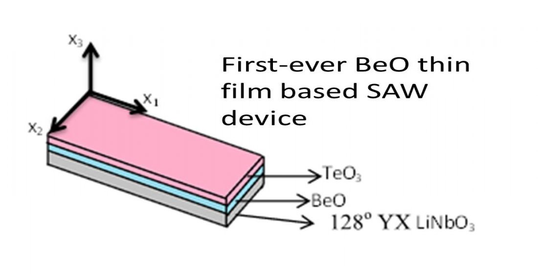
In the present study, the SAW propagation characteristics of proposed multi-layered structure are calculated using the SAW Analysis software (MSDOS (version 2 or later), IEEE, Montreal, QC, Canada) developed by Farnell and Adler [13,14]. The structure consists of BeO thin film integrated over 128° YX LiNbO3 single crystal and TeO3 over layer placed on BeO thin film. The multi-layered structure and the coordinate system are presented in Figure 1.
The Cartesian coordinate system is chosen in such a way that Rayleigh wave propagates along —axis in which its amplitude vanishes as tends to negative infinity, and —axis is parallel to the direction of particle polarization.
The electric potential and particle displacements in a piezoelectric medium are governed by the following elastic wave equations [1,13]:
where is the mechanical stiffness tensor, is the dielectric permittivity tensor, is the piezoelectric tensor, and is the density of the medium. The material parameters, like density, elastic constant, piezoelectric constant, and dielectric constants at a given temperature of TeO3, Wurtzite BeO thin films, and 128° YX LiNbO3 single crystal used in present study to estimate the SAW phase velocity of the layered structure, are taken from earlier reported data by Dewan et al., Duman et al., Cline et al., and Kovacs et al., respectively [12,18,22,23], and are presented in Table 1.
2.1. Electromechanical Coupling Coefficient
2.2. Temperature Coefficient of Delay (TCD)
The temperature dependence of SAW device is expressed in terms of TCD given by [1,26,27]
where is the coefficient of thermal expansion of base layer, and are the SAW velocities of the layered structure at respective temperatures. The TCD is measured in the units of ppm °C−1.
Using the material parameters listed in Table 1, the authors obtained the SAW phase velocity for the multi-layered structure through the software. The coupling coefficient and TCD were consequently calculated using the SAW velocity so obtained in Equations (3) and (4).
3. Results and Discussion
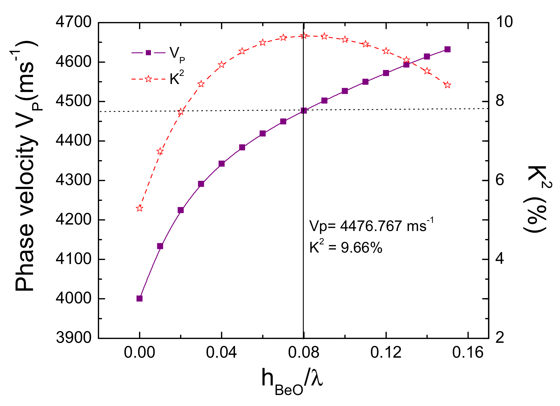
The SAW phase velocity (), electromechanical coupling coefficient and temperature coefficient of delay of bilayer BeO/128° YX LiNbO3 SAW structure were first calculated as a function of normalized thickness of BeO over layer, where is the BeO over layer thickness, and is the acoustic wavelength.
The change in SAW phase velocity () and electromechanical coupling coefficient with the normalized thickness of BeO over layer is shown in Figure 2. It is found that the SAW phase velocity increases from 3800 ms−1 (SAW velocity of bare 128° YX LiNbO3 single crystal) to 4476 ms−1 with increase in the BeO over layer thickness from 0 to 0.08 λ. The enhanced SAW velocity is principally due to the higher velocity (7800 ms−1) of BeO film in comparison to LiNbO3, and with the increasing over layer thickness of BeO, SAW energy is assembled more into BeO [9].
Figure 2 shows the rise in the value of electromechanical coupling coefficient for BeO/128° YX LiNbO3 bilayer structure. The value of increases nearly twofold, i.e., from ∼5% ( of bare 128° YX LiNbO3 single crystal) to ∼9.66% with the change in BeO over layer thickness from 0 to 0.08 λ. And with further increase in the BeO over layer thickness (beyond 0.08 λ), its value decreases. The significant rise in the value of coupling coefficient with the integration of a BeO over layer (in the range 0 to 0.08 λ) on the top of LiNbO3 single crystal is accounted to the stiffening effect produced by the over layer [28]. The stiffened layer escalates the stress and raises the potential at the interface [29]. Thus, in addition to the piezoelectric coefficients, stress also makes a noteworthy contribution in raising the electric potential and thereby augments the coupling coefficient. With the increase in the over layer thickness from 0.08 λ to 0.15 λ, the value of reduces to ∼8% from 9.7% because, at greater thickness, the impact of mass loading influences the propagation [28].
The temperature coefficient of delay for the BeO/128° YX LiNbO3 bilayer structure is calculated using Equation (4), and its dispersion with normalized BeO over layer thickness is shown in the Figure 3. It is found to reduce a little from 76 to ∼66 ppm °C−1 with an increase in the BeO over thickness from 0 λ to 0.08 λ. The small reduction in the value of TCD is credited to the fact that BeO film has comparatively lower but positive TCD value than for LiNbO3 crystal [24]. And with the addition of greater BeO over layer thickness, the SAW energy is more accumulated in BeO; hence, it exhibits the reduced value of TCD for BeO/128° YX LiNbO3 bilayer structure. It can be inferred from Figure 3 that the BeO/128° YX LiNbO3 bilayer structure is thermally unstable as both LiNbO3 and BeO are positive TCD materials. The positive TCD BeO/128° YX LiNbO3 bilayer structure can be made temperature stable by integrating it with an over layer (i.e., SiO2 and TeO3) possessing negative TCD [21,29,30,31]. Previously reported results show that in comparison to SiO2, TeO3 thin films possess high value of negative TCD [18,20,21,30,31]. So, with the integration of relatively less thick TeO3 over layer, a positive TCD device can be made temperature stable [18,19].
Therefore, in the present study, the result of adding TeO3 over layer over BeO/128° YX LiNbO3 bilayer structure on its SAW propagation characteristics have been investigated further. In TeO3/BeO/128° YX LiNbO3 multi- layered SAW structure, the thickness of BeO layer is fixed at 0.08 λ because it is observed in Figure 2 that, at this BeO over layer thickness, the BeO/128° YX LiNbO3 bilayer structure has maximum value of (∼9.66%) and appreciable phase velocity (∼4467 ms−1).
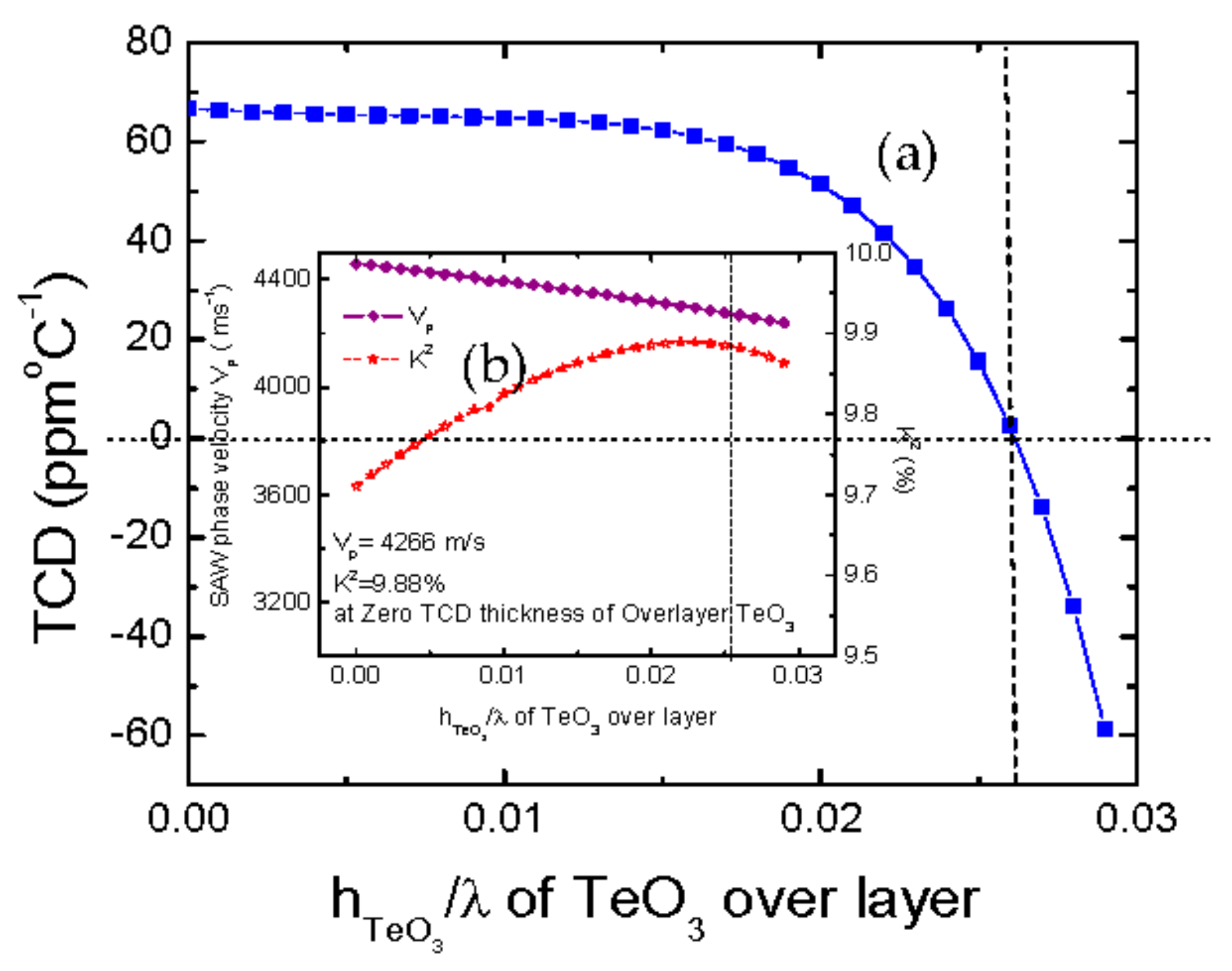
Figure 4 presents the TCD variation of TeO3/BeO (0.08 λ)/128° YX LiNbO3 multi-layered SAW structure as a function of normalized thickness of TeO3 over layer, where is the TeO3 over layer thickness. The TCD of TeO3/BeO(0.08 λ)/128° YX LiNbO3 layered structure reduces to 0 from 66 ppm °C−1 with an increase in the (negative TCD) TeO3 over layer thickness from 0 to 0.026 λ. Thus, a temperature stable TeO3/BeO(0.08 λ)/128° YX LiNbO3 multi-layered SAW device can be achieved with the integration of 0.026 λ thick TeO3 over layer.
The effect of integrating TeO3 over layer is examined on SAW phase velocity and , as well. The inset in Figure 4b shows the change of and SAW phase velocity for TeO3/BeO (0.08 λ)/128° YX LiNbO3 with the normalized thickness of TeO3 over layer. It may be seen that the value of SAW phase velocity declines faintly from 4467 to 4266 ms−1 with an increase in the TeO3 over layer thickness from 0 to 0.026 λ owing to the point that TeO3 has lower SAW phase velocity in comparison to BeO(0.08 λ)/128° YX LiNbO3 bilayer structure. Moreover, with the rise in the TeO3 over layer thickness from 0 to 0.026 λ, the value of increases further from 9.66% to ∼9.85%. This is because the thickness of TeO3 over layer is much less than the acoustic wavelength leading to the stiffening and further increase in the potential and hence electromechanical coupling coefficient [21,28]. It may be noted that the introduction of 0.026 λ thick TeO3 over layer in BeO (0.08 λ)/128°YX LiNbO3 bilayer structure not only marginally increases the value of (from 9.70% to 9.85%) but also makes the device temperature stable. With the further increase in the TeO3 over layer thickness, the TCD of TeO3/BeO (0.08 λ)/128° YX LiNbO3 multi-layered SAW structure becomes negative, making the device temperature unstable again. Hence the optimum thickness of TeO3 over layer is taken to be 0.026 λ. Therefore, a temperature stable TeO3 (0.026 λ)/BeO(0.08 λ)/128° YX LiNbO3 multi-layered SAW structure with high value of (∼9.85%) and the phase velocity (∼4266 ms−1) is proposed, which is suitable for its applications in narrow band filters in GHz range.
4. Conclusions
In the present work the SAW propagation properties of TeO3/BeO/128° YX LiNbO3 multi-layered SAW structure have been investigated theoretically. The optimized thickness values of TeO3 and BeO thin films are obtained. It is established that with the integration of (0.026 λ) TeO3 and (0.08 λ) BeO layer on 128° YX LiNbO3 single crystal, an efficient, temperature stable, high velocity (∼4266 ms−1) multi-layered SAW structure can be made. Because the proposed device is based upon sturdy wurtzite BeO layer, it can work efficiently in the severe environment conditions. The proposed temperature stable SAW structure can be conceived effortlessly for possible applications in both high, as well as low, frequency regions.
Author Contributions
Conceptualization, N.D.S.; Formal analysis, N.D.S.; Investigation, N.D.S.; Methodology, N.D.S.; Software, J.B.; Writing—original draft, N.D.S.; Writing—review & editing, J.B. All authors have read and agreed to the published version of the manuscript.
Funding
This research received no external funding.
Institutional Review Board Statement
Not applicable.
Informed Consent Statement
Not applicable.
Conflicts of Interest
The authors declare no conflict of interest.
References
- Luo, J.T.; Quan, A.J.; Liang, G.X.; Zheng, Z.H.; Ramadan, S.; Fu, C.; Li, H.L.; Fu, Y.Q. Love-mode surface acoustic wave devices based on multilayers of TeO2/ ZnO(1 1 2 0)/Si(1 0 0) with high sensitivity and temperature stability. Ultrasonics 2017, 75, 63–70. [Google Scholar] [CrossRef] [PubMed]
- Fan, L.; Zhang, S.; Ge, H.; Zhang, H. Theoretical investigation of acoustic wave devices based on different piezoelectric films deposited on silicon carbide. J. Appl. Phys. 2013, 114, 024504. [Google Scholar] [CrossRef]
- Naumenko, N.; Nicolay, P. AlN/Pt/LN structure for SAW sensors capable of operating at high temperature. Appl. Phys. Lett. 2017, 111, 073507. [Google Scholar] [CrossRef]
- Liang, J.; Yang, X.; Zheng, S.; Sun, C.; Zhang, M.; Zhang, H.; Zhang, D.; Pang, W. Modulation of acousto-electric current using a hybrid on-chip AlN SAW/GFET device. Appl. Phys. Lett. 2017, 110, 243504. [Google Scholar] [CrossRef]
- Gillinger, M.; Shaposhnikov, K.; Knobloch, T.; Schneider, M.; Kaltenbacher, M.; Schmid, U. Impact of layer and substrate properties on the surface acoustic wave velocity in scandium doped aluminum nitride based SAW devices on sapphire. Appl. Phys. Lett. 2016, 108, 231601. [Google Scholar] [CrossRef]
- Go, D.B.; Atashbar, M.Z.; Ramshani, Z.; Chang, H.-C. Surface acoustic wave devices for chemical sensing and microfluidics: A review and perspective. Anal. Methods 2017, 9, 4112–4134. [Google Scholar] [CrossRef]
- Delsing, P.; Cleland, A.N.; Schuetz, M.J.; Knörzer, J.; Giedke, G.; Cirac, J.I.; Srinivasan, K.; Wu, M.; Balram, K.C.; Bäuerle, C.; et al. The 2019 surface acoustic waves roadmap. J. Phys. D Appl. Phys. 2019, 52, 353001. [Google Scholar] [CrossRef]
- Campbell, C. Surface Acoustic Wave Devices for Mobile and Wireless Communications, Four-Volume Set; Academic Press: San Diego, CA, USA; Toronto, ON, Canada, 1998. [Google Scholar]
- Collins, H.; Hagon, P.J.; Pulliam, G.R. Evaluation of new single crystal piezoelectric materials for surface acoustic –wave applications. Ultrasonics 1970, 8, 218–226. [Google Scholar] [CrossRef]
- Lee, S.M.; Jang, Y.; Yum, J.H.; Larsen, E.S.; Lee, W.C.; Kim, S.K.; Bielawski, C.W.; Oh, J. Crystal Properties of atomic- layer deposited beryllium oxide on crystal and amorphous substrates. Semicond. Sci. Technol. 2019, 34, 115021. [Google Scholar] [CrossRef]
- Koh, D.; Yum, J.H.; Banerjee, S.K.; Hudnall, T.W.; Bielawski, C.; Lanford, W.A.; French, B.L.; French, M.; Henry, P.; Li, H.; et al. Investigation of atomic layer deposited beryllium oxide material properties for high K dielectric applications. J. Vac. Sci. Technol. B 2014, 32, 03D117. [Google Scholar] [CrossRef]
- Duman, S.; Sutlu, A.; Bagci, S.; Tutuncu, H.M.; Srivastava, G.P. Structural, elastic, electronic and phonon properties of zinc blende and wurtzite BeO. J. Appl. Phys. 2009, 105, 033719. [Google Scholar] [CrossRef]
- Farnell, G.W.; Adler, E.L. Elastic Wave Propagation in Thin Layers. In Physical Acoustics Principles and Methods; Mason, W.P., Thurston, R.N., Eds.; Academic Press: New York, NY, USA, 1972; Volume 9, pp. 35–127. [Google Scholar]
- Farnell, G.W.; Adler, E.L. Multilayer acoustic surface wave program. Proc. Inst. Electr. Eng. 1995, 122, 470–471. [Google Scholar]
- Nakahata, H.; Fujii, S.; Higaki, K.; Hachigo, A.; Kitabayashi, H.; Shikata, S.; Fujimori, N. Diamond-based surface acoustic wave devices. Semicond. Sci. Technol. 2003, 18, 96–104. [Google Scholar] [CrossRef]
- Zhou, C.; Yang, Y.; Zhan, J.; Ren, T.; Wang, X.; Tian, S. Surface acoustic wave characteristics based on c-axis (006) LiNbO3/diamond/silicon layered structure. Appl. Phys. Lett. 2011, 99, 022109. [Google Scholar] [CrossRef]
- Benetti, M.; Cannat’a, D.; Pietrantonio, F.D.; Verona, E. Growth of AlN piezoelectric film on diamond for high-frequency surface acoustic wave devices. IEEE Trans. Ultrason. Ferroelectr. Freq. Control 2005, 52, 1806. [Google Scholar] [CrossRef] [PubMed]
- Dewan, N.; Sreenivas, K.; Gupta, V. Temperature-Compensated Devices Using Thin TeO2 Layer with Negative TCD. IEEE Electron Device Letters 2006, 27, 752–754. [Google Scholar] [CrossRef]
- Cacho VD, D.; Siarkowski, A.L.; Morimoto, N.I.; Borges, B.V.; Kassab, L.R. Fabrication and Characterization of TeO2-ZnO Rib Waveguides. ECS Trans. 2010, 31, 225–229. [Google Scholar] [CrossRef]
- Dewan, N.; Sreenivas, K.; Gupta, V.; Katiyar, R.S. Growth of amorphous TeOx (2 ≤ x ≤ 3) thin film by radio frequency sputtering. J. Appl. Phys. 2007, 101, 084910. [Google Scholar] [CrossRef]
- Dewan, N.; Tomar, M.; Gupta, V.; Sreenivas, K. Temperature stable LiNbO3 surface acoustic wave device with diode sputtered amorphous TeO2 over-layer. Appl. Phys. Lett. 2005, 86, 223508. [Google Scholar] [CrossRef]
- Cline, C.F.; Dunegan, H.L.; Henderson, G.W. Elastic Constants of Hexagonal BeO, ZnS and CdSe. J. Appl. Phys. 1967, 38, 1944–1948. [Google Scholar] [CrossRef]
- Kovacs’s, G.; Anhorn, M.; Engan, H.E.; Visintini, G.; Ruppel, C.C.W. Improved material constants for LiNbO3 and LiTaO3. IEEE Symp. Ultrason. 1990, 1, 435–438. [Google Scholar]
- Sirota, N.N.; Kuzmina, A.M.; Orlova, N.S. Debye- Waller factors and Elastic constants for Beryllium oxide at temperature between 10 and 720 K. Cryst. Res. Technol. 1992, 27, 711–716. [Google Scholar] [CrossRef]
- Smith, R.T.; Welsh, F.S. Temperature Dependence of the Elastic, Piezoelectric, and Dielectric Constants of Lithium Tantalate and Lithium Niobate. J. Appl. Phys. 1971, 42, 2219–2230. [Google Scholar] [CrossRef]
- Soni, N.D. SAW propagation characteristics of TeO3/3C-SiC/LiNbO3 layered structure. Mater. Res. Express 2018, 5, 046309. [Google Scholar]
- Rana, L.; Gupta, V.; Soni, N.D.; Tomar, M. SAW field and acousto-optical interaction in ZnO/AlN/sapphire structure. In Proceedings of the 2016 Joint IEEE International Symposium on the Applications of Ferroelectrics, European Conference on Application of Polar Dielectrics, and Piezoelectric Force Microscopy Workshop (ISAF/ECAPD/PFM), Darmstadt, Germany, 21–25 August 2016. [Google Scholar]
- Shih, W.C.; Wang, T.L.; Hsu, L.L. Surface acoustic wave properties of aluminum oxide films on lithium Niobate. Thin Solid Film. 2010, 518, 7143–7146. [Google Scholar]
- Tomar, M.; Gupta, V.; Sreenivas, K.; Mansingh, A. Temperature stability of ZnO thin film SAW device on fused quartz. IEEE Trans. Device Mater. Reliab. 2005, 5, 494–500. [Google Scholar] [CrossRef]
- Gupta, V.; Tomar, M.; Sreenivas, K. Improved temperature stability of LiNbO3 surface acoustic wave devices with sputtered SiO2 over-layers. Ferroelectrics 2005, 329, 57–60. [Google Scholar] [CrossRef]
- Zhou, F.M.; Li, Z.; Fan, L.; Zhang, S.Y.; Shui, X.J.; Wasa, K. Effects of TeOx films on temperature coefficients of delay of Love type wave devices based on TeOx/ 36° YX—LiTaO3 structures. Vaccuum 2010, 84, 986–991. [Google Scholar] [CrossRef]
Figure 1.
Illustration of TeO3/Beryllium Oxide (BeO)/128° YX LiNbO3 multilayer surface acoustic wave (SAW) structure and the coordinate system.
Figure 1.
Illustration of TeO3/Beryllium Oxide (BeO)/128° YX LiNbO3 multilayer surface acoustic wave (SAW) structure and the coordinate system.

Figure 2.
Variation of SAW phase velocity and electromechanical coupling coefficient with normalized thickness of BeO over layer in BeO/128° YX LiNBO3 SAW layered structure.
Figure 2.
Variation of SAW phase velocity and electromechanical coupling coefficient with normalized thickness of BeO over layer in BeO/128° YX LiNBO3 SAW layered structure.

Figure 3.
Variation of temperature coefficient of delay (TCD) with normalized thickness of BeO over layer in BeO/128° YX LiNBO3 SAW layered structure.
Figure 3.
Variation of temperature coefficient of delay (TCD) with normalized thickness of BeO over layer in BeO/128° YX LiNBO3 SAW layered structure.

Figure 4.
(a): Variation of TCD of TeO3/BeO(0.08 λ)/128° YX LiNbO3 SAW structure with normalized thickness of TeO3 over layer. (b) Variation of phase velocity and for TeO3/BeO(0.08 λ)/128° YX LiNbO3 SAW structure with normalized thickness of TeO3 over layer.
Figure 4.
(a): Variation of TCD of TeO3/BeO(0.08 λ)/128° YX LiNbO3 SAW structure with normalized thickness of TeO3 over layer. (b) Variation of phase velocity and for TeO3/BeO(0.08 λ)/128° YX LiNbO3 SAW structure with normalized thickness of TeO3 over layer.


Table 1.
Material constants and temperature coefficients used in simulations.
| Material Constants | Materials | Temperature Coefficients (°C−1) | ||||
|---|---|---|---|---|---|---|
| TeO3 [18] | BeO [12,22] | LiNbO3 [23] | TeO3 [18] | BeO [24] | LiNbO3 [25] | |
| Elastic Constants(1011 N/m2) | × 10−4 | |||||
| C11 | 0.14 | 4.606 | 1.98 | 0.06 | −2.63 | −1.74 |
| C33 | 4.916 | 2.279 | −1.34 | −1.53 | ||
| C66 | 1.670 | 0.728 | −1.98 | −1.43 | ||
| C44 | 0.265 | 1.477 | 0.5965 | 0.0646 | −0.95 | −2.04 |
| C12 | 1.265 | 0.5472 | −4.27 | −2.52 | ||
| C13 | 0.8848 | 0.6513 | −39.8 | −1.59 | ||
| C14 | 0.0788 | −2.14 | ||||
| Piezoelectric constant (C/m2) | ||||||
| e33 | 0.0364 | 1.77 | 8.87 | |||
| e31 | −0.0735 | 0.30 | 2.21 | |||
| e15 | 3.69 | 1.47 | ||||
| e22 | 2.42 | 0.79 | ||||
| Dielectric constant (10−11 F/m) | ||||||
| 23.7 | 3.06 | 45.6 | 1.6 | 3.23 | ||
| 3.13 | 26.3 | 6.27 | ||||
| Density (Kg/m3) | ||||||
| 4578 | 3010 | 4628 | ||||
Publisher’s Note: MDPI stays neutral with regard to jurisdictional claims in published maps and institutional affiliations. |
© 2021 by the authors. Licensee MDPI, Basel, Switzerland. This article is an open access article distributed under the terms and conditions of the Creative Commons Attribution (CC BY) license (http://creativecommons.org/licenses/by/4.0/).
Share and Cite
MDPI and ACS Style
Soni, N.D.; Bhola, J. Enhanced Properties of SAW Device Based on Beryllium Oxide Thin Films. Crystals 2021, 11, 332. https://0-doi-org.brum.beds.ac.uk/10.3390/cryst11040332
AMA Style
Soni ND, Bhola J. Enhanced Properties of SAW Device Based on Beryllium Oxide Thin Films. Crystals. 2021; 11(4):332. https://0-doi-org.brum.beds.ac.uk/10.3390/cryst11040332
Chicago/Turabian StyleSoni, Namrata Dewan, and Jyoti Bhola. 2021. "Enhanced Properties of SAW Device Based on Beryllium Oxide Thin Films" Crystals 11, no. 4: 332. https://0-doi-org.brum.beds.ac.uk/10.3390/cryst11040332
Note that from the first issue of 2016, this journal uses article numbers instead of page numbers. See further details here.