Article

AgSn[Bi1−xSbx]Se3: Synthesis, Structural Characterization, and Electrical Behavior

by
Paulina Valencia-Gálvez
1,
Daniela Delgado
1,
María Luisa López
2,
Inmaculada Álvarez-Serrano
2,
Silvana Moris
3,* and
Antonio Galdámez
1,*
1
Departamento de Química, Facultad de Ciencias, Universidad de Chile, Las Palmeras 3425, Santiago 7800003, Chile
2
Departamento de Química Inorgánica, Facultad de Ciencias Químicas, Universidad Complutense, 28040 Madrid, Spain
3
Centro de Investigación de Estudios Avanzados del Maule (CIEAM), Vicerrectoría de Investigación y Postgrado, Universidad Católica del Maule, Avenida San Miguel 3605, Talca 3480112, Chile
*
Authors to whom correspondence should be addressed.
Submission received: 13 June 2021 / Revised: 22 July 2021 / Accepted: 23 July 2021 / Published: 26 July 2021
(This article belongs to the Special Issue Robust Microelectronic Devices)

Abstract

:
Herein, we report the synthesis, characterization, and electrical properties of lead-free AgSnm[Bi1−xSbx]Se2+m (m = 1, 2) selenides. Powder X-ray diffraction patterns and Rietveld refinement data revealed that these selenides consisted of phases related to NaCl-type crystal structure. The microstructures and morphologies of the selenides were investigated by backscattered scanning electron microscopy, energy-dispersive X-ray spectroscopy, and high-resolution transmission electron microscopy. The studied AgSnm[Bi1−xSbx]Se2+m systems exhibited typical p-type semiconductor behavior with a carrier concentration of approximately ~+1020 cm−3. The electrical conductivity of AgSnm[Bi1−xSbx]Se2+m decreased from ~3.0 to ~10−3 S·cm−1 at room temperature (RT) with an increase in m from 1 to 2, and the Seebeck coefficient increased almost linearly with increasing temperature. Furthermore, the Seebeck coefficient of AgSn[Bi1−xSbx]Se3 increased from ~+36 to +50 μV·K−1 with increasing Sb content (x) at RT, while its average value determined for AgSn2[Bi1−xSbx]Se4 was approximately ~+4.5 μV·K−1.

1. Introduction

The multicomponent silver chalcogenide family AgM1M2Q3 (M1 = Pb, Sn; M2 = Bi, Sb, and Q = S, Se, Te) contains several thermoelectric phases [1,2,3,4,5,6,7]. Kanatzidis et al. extensively investigated the properties of chalcogenide compounds, which represent promising thermoelectric materials [8,9,10]. In particular, AgPbmSbTe2+m, Ag1.33Pb1.33Sb1.33Te4, and AgPb18SbSe20 were examined in detail. AgPbmSbTe2+m is a class of candidates for thermoelectric materials, which is often abbreviated as LAST (lead, antimony, silver, tellurium)-m. These compounds can be envisioned as an alloy between two cubic chalcogenides, PbTe- and AgSbTe2: (PbTe)m–AgSbTe2. Electrical transport studies have shown that the thermoelectric properties of this system can be fine-tuned via compositional parameter m. Recently, Dutta et al. and Cai et al. reported the thermoelectric properties of n-type AgPbBiSe3 and p-type AgPbmSbSe2+m families [11,12]. These phases possess high Seebeck coefficients S equal to approximately −131 μV·K−1 (AgPbBiSe3) and +130 μV·K−1 (AgPbmSbSe2+m; m = 10). In addition, AgPbBiSe3 exhibits S values of −131 and –204 μV·K−1 at 296 and 770 K, respectively, and electrical conductivity σ of 63 S·cm−1 at room temperature (RT) and 72 S·cm−1 at 818 K. As expected, these values increased with an increase in the halogen doping concentration. Experimental single-crystal X-ray diffraction (XRD) and high-resolution transmission electron microscopy (HRTEM) studies revealed that the electrical properties of these chalcogenides were related to the presence of nanoscopic inhomogeneities [4,13,14]. Electron diffraction and energy-dispersive X-ray spectroscopy (EDS) analyses demonstrated that Ag-Sb-rich nanostructures were embedded into the PbTe lattice of (PbTe)m–AgSbTe2 systems, whose electronic behaviors were sensitive to their microstructures.
Owing to the strict environmental regulations related to the use of lead-based materials, novel compounds, such as lead-free p-type AgSnSbSe3, n-type BiAgSeS, p-type (SnTe)m–AgSbTe2, p-type AgSnmSbSe2Tem, and (SnTe)m–AgBiTe2 systems, have been prepared recently [15,16,17,18,19,20,21]. (SnTe)m–AgBiTe2 systems could be viewed as alloys of two cubic chalcogenides, SnTe and AgBiTe2. These chalcogenides possess low thermal conductivities and large positive Seebeck coefficients. The influence of chemical substitution on the thermoelectric properties of the listed chalcogenides has been discussed in several studies. For example, the chemical substitution of Se by Te in AgSnSbSe3 (e.g., AgSnSbSe1.5Te1.5) results in the formation of a material with an average power factor S2·σ of ~9.54 μW·cm−1·K−2 (400–778 K) [15]. Herein, we report the synthesis, characterization, and electrical properties of novel lead-free AgSnm[Bi1−xSbx]Se2+m (m = 1 and 2) systems obtained via the isoelectronic substitution of Bi by Sb atoms. AgSnm[Bi1−xSbx]Se2+m compounds could be considered alloys of SnSe and Ag(Bi1−xSbx)Se2, corresponding to (SnSe)m–Ag(Bi1−xSbx)Se2 systems. Tan et al. suggested that bismuth was a better neutralizer of positive holes in the SnTe structure than antimony [18]. In this study, we investigated the electrical and structural characteristics of selenides that were selected because bismuth was a more efficient electron donor than antimony. Powder X-ray diffraction patterns and Rietveld refinement results were consistent with phases related to the cubic NaCl-type lattice. The microstructures and morphologies of these systems were investigated using scanning electron microcopy (SEM) and high-resolution transmission electron microscopy (HRTEM).

2. Materials and Methods

Silver powder (99.99% purity, Sigma-Aldrich, St. Louis, MO, USA), antimony powder (99.99% purity, Sigma-Aldrich, St. Louis, MO, USA), tin powder (99.9% purity, Sigma-Aldrich, St. Louis, MO, USA), selenium powder (99.99% purity, Sigma-Aldrich, St. Louis, MO, USA), bismuth powder (99.99% purity, Merck, Kenilworth, NJ, USA), and sulfur powder (99.99% purity, Merck, Kenilworth, NJ, USA) were used in this study. All experiments were performed under a dry and oxygen-free argon atmosphere. Selenide phases with the nominal compositions were prepared via the solid-state reaction of Ag, Sn, Bi, Sb, and Se powders mixed in the stoichiometric proportions inside evacuated quartz ampoules. The reaction mixture was gradually heated to 1223 K at a rate of +50 K/h, maintained at this temperature for ~12 h, and slowly cooled to RT at 8 K/h. Chemical compositions of the samples were determined by scanning electron microscopy (SEM, JEOL 5400 system, Tokyo, Japan) and energy-dispersive X-ray spectroscopy (EDS, Oxford LinK ISIS microanalyzer, Oxford Instruments, Abingdon, UK). XRD patterns were obtained at RT using a Bruker D8 advanced powder diffractometer (Bruker, Billerica, MA, USA) with CuKα radiation over the 2θ range of 5–80° at a step size of 0.01°. In addition, XRD patterns were also collected at temperatures varying from RT to 77 K using a PANalytical X’Pert PROMPD diffractometer (CuKα1 = 1.544426 Å, CuKα2 = 1.54098 Å) over the 2θ range of 5–80° at a step size of 0.0167° (Malvern Panalytical, Boulder, CO, USA). The diffractometer was equipped with a heating chamber (Anton Paar HTK1200, PANanalytical BV, Boulder, CO, USA). The collected data were analyzed by two Rietveld refinement software programs: Fullprof and MAUD [22,23,24]. A standard LaB6 sample was used to measure instrumental profiles. SEM–EDS and powder XRD analyses revealed that the AgSnm[Bi1−xSbx]Se2+m (m = 1 and 2) samples have been successfully prepared. On the other hand, reaction products with the nominal stoichiometry of AgSnm[Bi1−xSbx]Sem+2 (m = 4, 8, 10, and 12) included 10–30% SnSe impurities. For example, the reaction products with the nominal compositions AgSn8[Bi0.8Sb0.2]Se10 and AgSn4[Bi0.2Sb0.8]Se6 contained AgSnMSe3, SnSe, and some unidentified impurities. Differential thermal analysis (DTA) and thermogravimetric analysis (TGA) of the samples were performed using a Rheometric Scientific STA 1500H/625 thermal analysis system (Rheometric Scientific, Inc., Piscataway, NJ, USA). To record DTA/TGA curves, the samples were heated from RT to 1273 K in an argon atmosphere or to 673 K in air at a rate of 10 K/min. A high-temperature melting method was applied to obtain suitable ingot samples for Seebeck measurements. The obtained reaction samples were crushed into powders and placed into a quartz ampoule, which was evacuated and flame-sealed under an argon atmosphere. This tube was then placed into a furnace at 1073 K for ~2 h and then slowly cooled to RT at 8 K/h. Subsequently, these ingots were cut and polished for measurements of their transport properties. Although various experimental conditions (temperature, cooling rate, melting, and cooling) were utilized, the ingots of some chemical compositions of AgSn2[Bi1−xSbx]Se4 and AgSn[Bi1−xSbx]Se3 were too brittle and broken. In the case of the AgSn2[Bi1−xSbx]Se4 composition, a visible change in the pellet appearance (the presence of small holes on the pellet surface) was observed in some samples during thermal cycling. Electrical conductivities of the samples were measured by a pellet method, in which pellets were uniaxially pressed at 5 × 10⁸ Pa to form cylindrical specimens with diameters of ~7 mm and thicknesses of ~1–2 mm. The pelletized specimens were sintered at 673, 923, and 993 K for 12 and 24 h in an argon atmosphere (Ar 12 or 24 h) and in air at 673 K for 12 h (air 12 h). The low-temperature (20–300 K) Hall effect and Seebeck coefficient measurements were performed using a physical property measurement system (PPMS). High-temperature electrical conductivities were measured using an ECOPIA HMS 2000 system (ECOPIA, Anyang-city, Gyeonggi-do, South Korea) and Keithley 6220 current source/Keithley 2182A nanovoltmeter (Tektronix, Inc., Beaverton, OR, USA) with a four-probe contact geometry. High-temperature Seebeck coefficients were determined by a laboratory-made system. The densities of the ingot and pellet samples were computed from their dimensions and masses; the obtained magnitudes were equal to ~90–92% of the theoretical values.

3. Results and Discussion

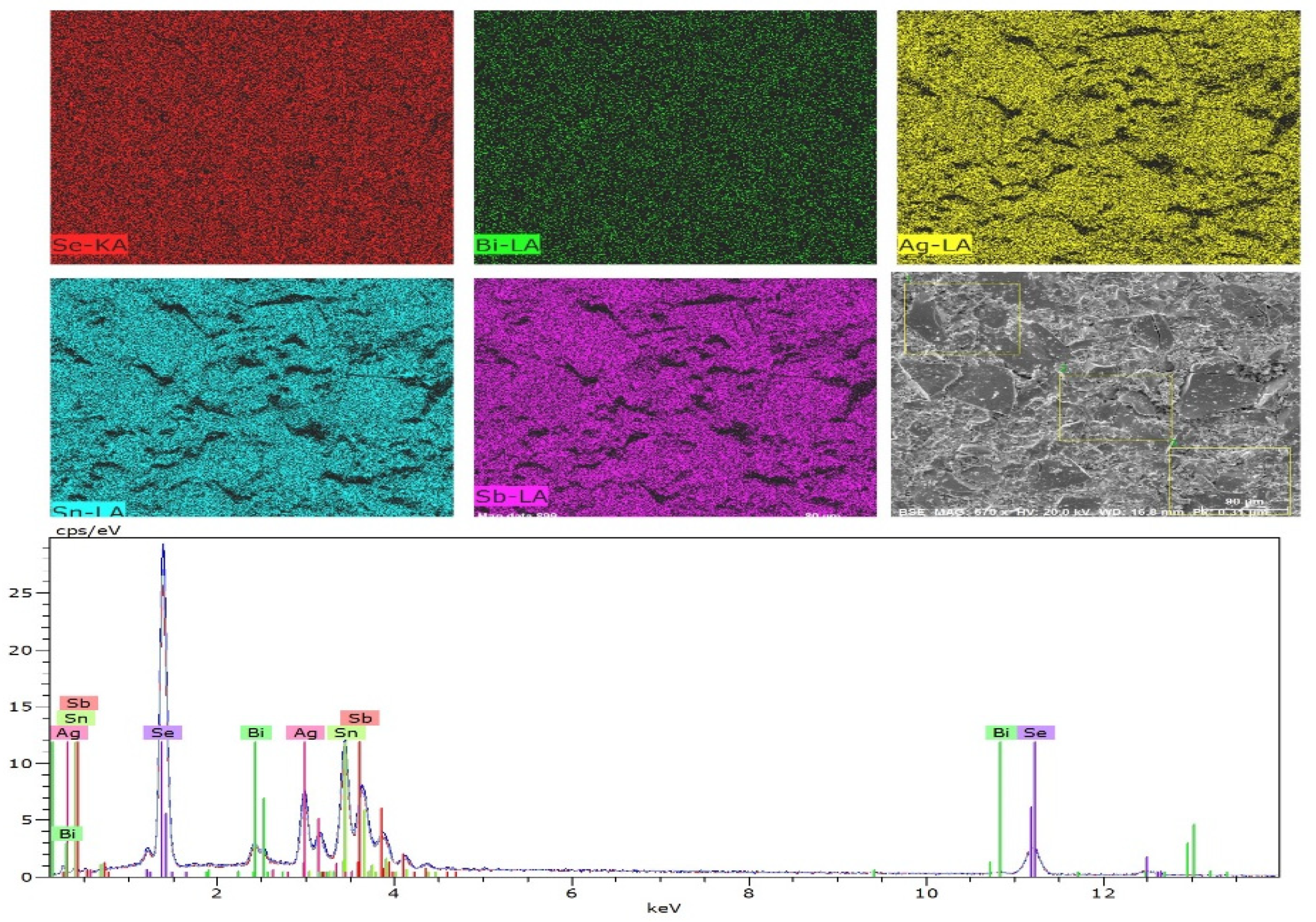
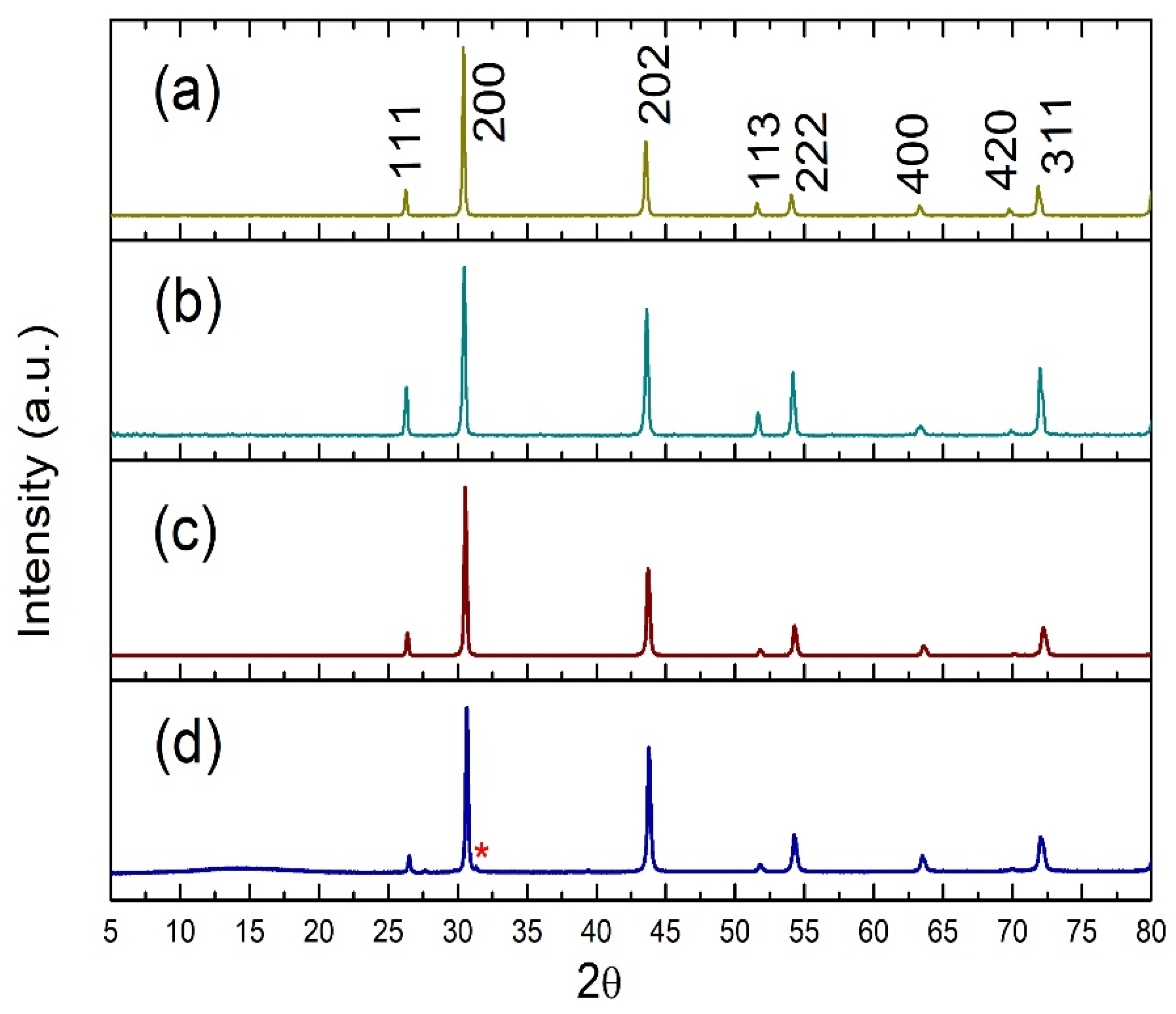
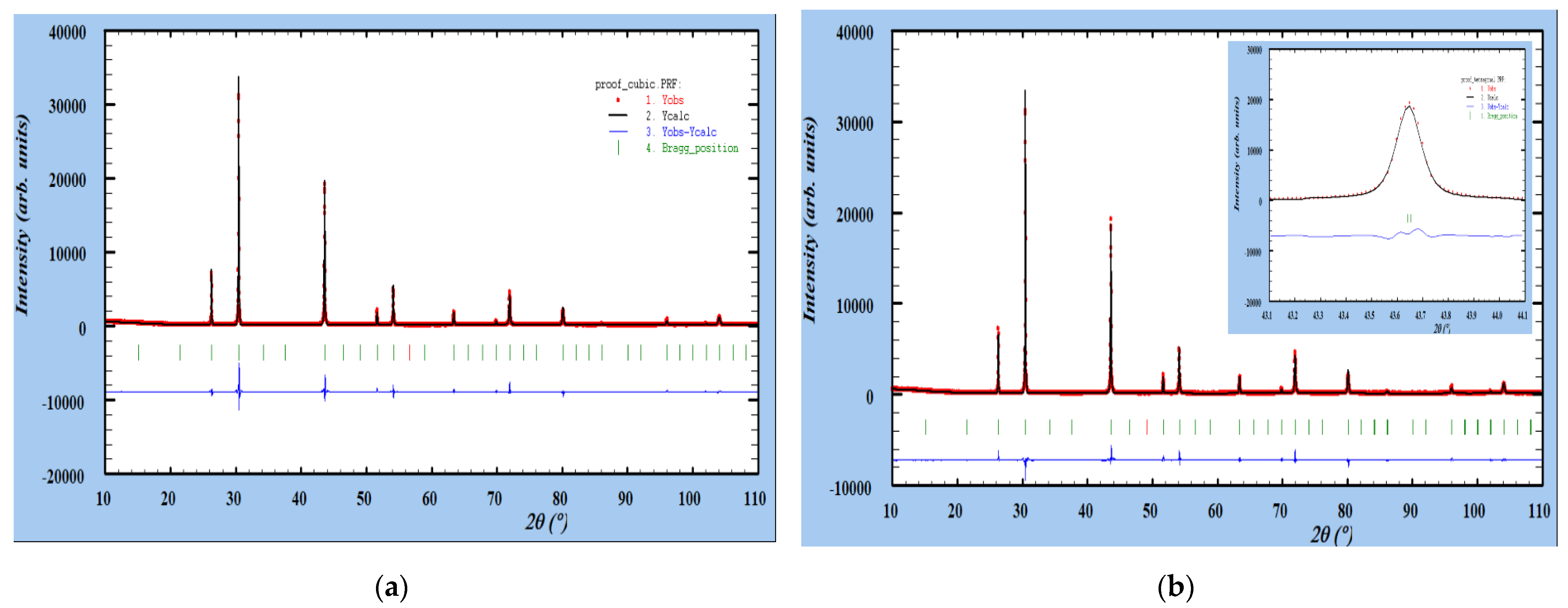
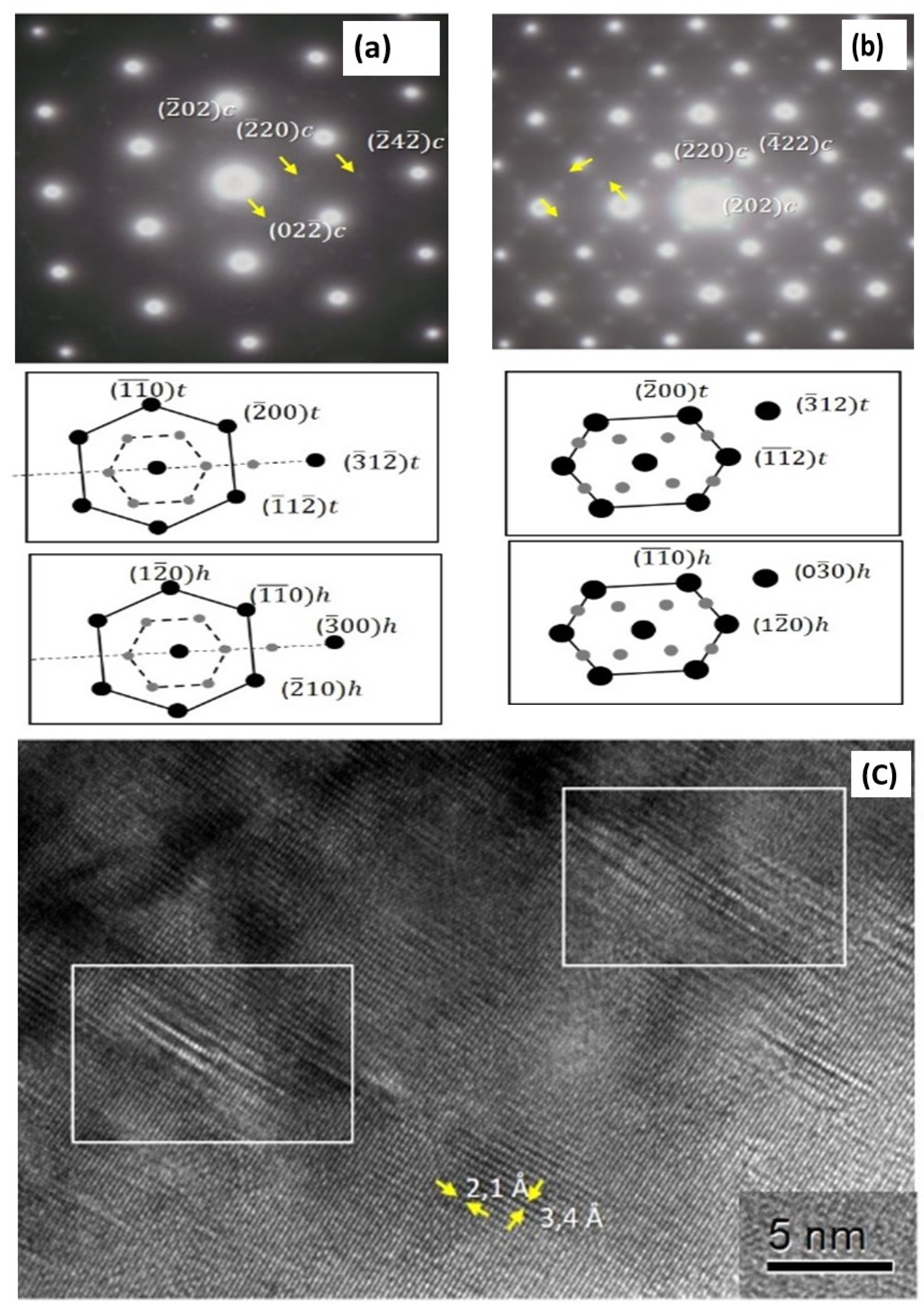
3.1. Structures and Compositions of Selenide Samples

The backscattered electron images and EDS analyses of the powder samples, ingots, and pellets for electrical measurements revealed that the chemical compositions of all selenide samples were uniform throughout the scanned region (Figure 1). No secondary intergranular phases were observed in the AgSn[Bi1−xSbx]Se3 samples (x = 0, 0.2, 0.3, 0.8) within the detection limits of this technique. Figure 2 presents the PXRD patterns for the AgSnm[Bi1−xSbx]Se2+m samples with m = 1 and 2. Their sharpness indicates high crystallinity, and the observed interlayer spacing was in good agreement with the calculated interplanar spacing d. The SEM–EDS and XRD analyses suggest that the prepared materials could be regarded as a continuous solid solution between SnSe and AgBiSe2, similarly to the SnTe–NaSbTe2 and SnTe–NaBiTe2 systems [25]. In the case of AgSn2[Bi1−xSbx]Se4 samples (m = 2), the PXRD patterns show an extremely small amount of SnSe impurities.
A structural analysis of the AgPbmSbTe2+m phases carried out by Quarez et al. by HRTEM analyses and single-crystal XRD demonstrated that the structure of these phases could be refined in the space group P m 3 ¯ m , as well as in a lower symmetric space group such as P4/mmm [13]. It is extremely complicated to choose the adequate symmetry since all refinements were acceptable due to the coherent X-ray scattering amplitudes, which are extremely similar, and the super-structure reflections in the powder pattern are especially hard to see.
The XRD patterns obtained for these phases were refined in the Pm-3m and P4/mmm space groups. In both space groups, the two sites at the (0,0,1/2) and (1/2,1/2,0) positions were fully occupied by Ag, Sb, Sn, or Bi atoms. The RT Rietveld refinement profiles of AgSnBiSe3 based on the cubic and tetragonal models are shown in Figure 3. The following unit cell parameters were obtained: cubic unit cell ac = 5.86180(6) Å, tetragonal (at = btac√2/2, ctac) unit cell at = 4.14365 (16), and ct = 5.8631(4) Å. The tetragonal model contained two cation sites (1b and 1c Wyckoff sites), which were fully occupied by the randomly distributed Ag, Sn, and Bi cations. Selenium atoms adopted close cubic packing at the 1a and 1d Wyckoff sites. Both structural models were consistent with the experimental data as well as with the obtained R factors; therefore, we were unable to identify the best structural model for this material (Tables S1 and S2). Moreover, AgBiSe2 and Ag(Bi,Sb)Se2 phases show interesting structural transitions with both temperature and composition. Thus, at room temperature the Sb-free samples have a hexagonal symmetry within the space group P m 3 ¯ 1 . As the Sb content increases, these phases show a rhombohedral symmetry ( R 3 ¯ m ) [26].
XRD patterns of AgSn[Bi1−xSbx]Se3 and AgSn2[Bi1−xSbx]Se4 were refined using the cubic and tetragonal models (Table S3 and Figure S1—see in Supplementary Materials). As expected, the cell volume increased slightly after replacing Bi atoms (radius: 1.63 Å) by Sb atoms (radius: 1.53 Å), and the resulting solid solutions did not obey Vegard’s law.
In order to analyze the microstructural features of the samples, a study by HRTEM and electron diffraction was also carried out. Small crystals with octahedral AgSnBiSe3 shapes were observed. The mean atomic compositions (determined from the EDS data) of the studied samples were similar to the expected compositions. Figure 4 displays the electron diffraction (ED) patterns obtained along [111]c zone axis for the different selected regions of the selenide samples. It shows that different contrast zones are predominant in the analyzed crystals, as shown in Figure 4.
The Miller indices are calculated considering a cubic symmetry in both models and they are indicated in the image. However, spots of weak intensity that are prohibited in the space group F m 3 ¯ m are clearly observed. It is noteworthy that these weak spots indicate the appearance of different symmetries. The new Miller indices can be obtained from the Equations (1) and (2) where the unit cell transformation from cubic to tetragonal or hexagonal were considered.
Equation (1): cubic to tetragonal.
ht = ½ (hckc)
Kt = ½ (hc + kc)
lt = lc
Equation (2): cubic to hexagonal
hh = ½ (−kc + lc)
Kh = ½ (hclc)
lh = hc + kc + lc
Thus, in the micrograph of Figure 4a, these weak spots would not be compatible with a P-type cubic lattice, nor with a tetragonal symmetry, as shown in the diagrams below the ED images. However, they would be compatible with a hexagonal symmetry. On the contrary, only a P m 3 ¯ m cubic space group seems to be consistent with the superstructure spots (Figure 4b). These results indicate that the AgSnBiSe3 phase exhibits nanoscopic inhomogeneities, in good agreement with those reported for similar phases [10,13,27]. In addition, nanoregions with different orientations or symmetries were detected (Figure 4c). This is consistent with the results reported previously [13].

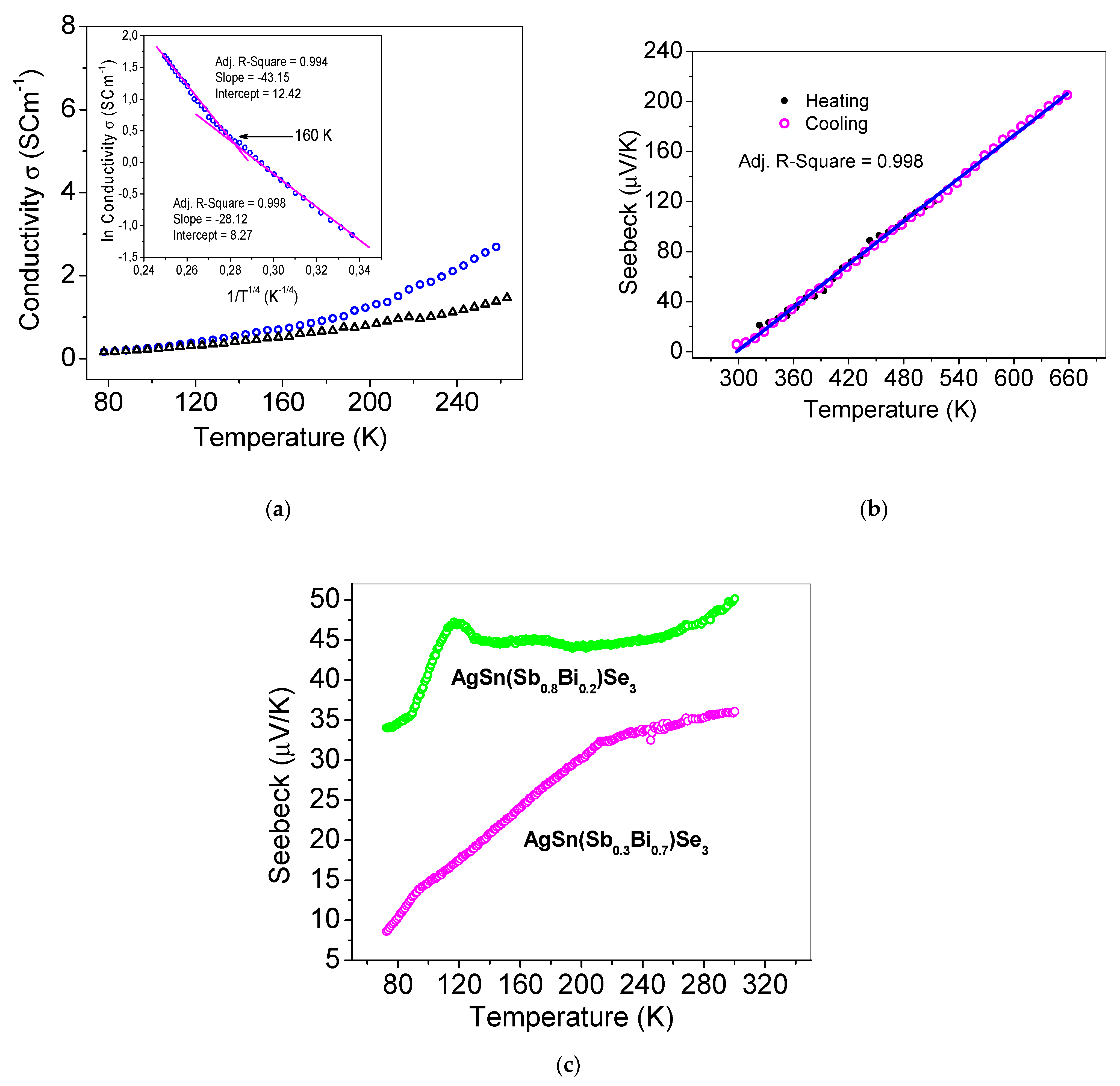
3.2. Electrical Properties and Seebeck Coefficients

The melting point of the prepared selenide samples was ~1000 K, and the pellets were sintered at 673, 923, and 993 K (see the experimental details). In addition, TGA was conducted in air from RT to 673 K to produce stable thermal and gravimetric signals. The obtained TGA results were consistent with the SEM–EDS and powder XRD data (Figures S2 and S3). The AgSn[Bi1−xSbx]Se3 pellets exhibited a microstructure with particle sizes of ∼2–14 μm and isolated regions with a grain size of ∼20 μm. The XRD patterns of the selenide samples recorded at various temperatures between RT and 77 K exhibit high structural and thermal stabilities (Figure S4). Their XRD and backscattered SEM–EDX analyses were performed after electrical measurements.
Figure 5a shows the temperature dependence of the electrical conductivity σ of the AgSnBiSe3 sample. For pristine AgSnBiSe3, electrical conductivity increases with increasing temperature, indicating the phase exhibits semiconductor behavior. The σ was thermally activated at low temperatures. In addition, the σ of the samples sintered at 923 K in Ar for 48 h was ~2.1 S·cm−1 at 240 K. This value was approximately two times higher than the σ of the samples sintered at 673 K in Ar or air (~1.1 S·cm−1) at 240 K. The AgSnBiSe3 sample with a cylindrical shape (ϕ~6.00 mm and s~1.0 mm) cut from the ingot of pristine material, exhibited an electrical conductivity of ~4.0 S·cm−1 at RT. The σ magnitudes obtained at 80 K and 140 K were equal to 0.24 and 0.75 S·cm−1, respectively. The electrical conductivity σ of AgSnm[Bi1−xSbx]Se2+m decreased from ~3.0 to 10−3 S·cm−1 at RT with an increase in m from 1 to 2 (Table 1). These values are comparable to those of AgSnmSbSem+2 (~10−3 − 93 S·cm−1 for m = 1–12) [15].
The low-temperature σ(T) of AgSnBiSe3 followed a standard variable range hopping (VRH) model described by the following equation:
σ = σ 0     e x p [ ( T 0 T ) 1 / 4 ]
where σ0 is the residual conductivity, and To is the characteristic temperature. To validate the VRH model, we fitted the experimental data with Equation (3). The obtained results presented in the inset of Figure 5a indicate that the transport mechanism regime involved the VRH process. The plot of ln σ versus T−1/4 changed its the slope at around ~160 K. The occurrence of the hopping process depends on the energy difference and relationship between the Fermi level and the mobility edge. This behavior was previously observed at low temperatures for other selenides, such as Pb-doped Cu2SnSe3 and CuyFe4Sn12X32 spinels [28,29].
The positive Seebeck coefficient values of the AgSnm[Bi1−xSbx]Se2+m systems (m = 1 and 2) obtained via the isoelectronic substitution of a fraction of Bi atoms with Sb indicates that holes are the dominant conduction carriers (Table 1). The temperature dependences of the Seebeck coefficient of AgSn[Bi1−xSbx]Se3 in the high-temperature and low-temperature ranges are shown in Figure 5b,c, respectively. The Seebeck coefficient of AgSn[Bi1−xSbx]Se3 (m = 1) selenides increased from ~+36 μV·K−1 (x = 0.2) to +50 μV·K−1 (x = 0.8) with increasing Sb content at RT. This value is approximately four times lower than that of AgSnSbSe3 (+179 μV·K−1) and is comparable with the Seebeck coefficient of SnTe at 300 K (+40 μV K−1). Consequently, the power factor (S2·σ) of AgSnBiSe3 was ~0.1 μW·cm−1·K−2. Power factors of 5–12 μW·cm−1·K−2 were obtained for AgSnmSbTem+2 systems at 300 K [21]. The S values of AgSn2[Bi1−xSbx]Se4 selenides increased from ~+3.9 (x = 0.2) to ~+4.9 μV·K−1 (x = 0.8) with an increase in the Sb content at RT (Table 1). The average Seebeck coefficient of the AgSn2[Bi1−xSbx]Se4 samples was ~+4.5 µV·K−1. This value is approximately ten times lower than that determined for AgSn[Bi0.2Sb0.8]Se3 (~+50 μV·K−1). Kanatzidis et al. reported that the Seebeck coefficients of p-type AgSnmSbSe2+m systems decreased from ~+179 to 51 μV·K−1 with an increase in m from 1 to 12 at RT [15]. The AgSn2[Bi1−xSbx]Se4 selenide samples exhibited S values of ~+92 μV·K−1 (x = 0.2) and +114 μV·K−1 (x = 0.8) at 450 K. The temperature dependence of S obtained for AgSn2[Bi1−xSbx]Se4 indicate degenerate semiconductor properties and is consistent with the behavior previously reported for AgSn10SbSe2Te10 [17].
The temperature dependence of the Seebeck coefficient of degenerate semiconductors is expressed by the formula
S = [ 8 π 2 / 3 k B 2 ( r + 3 / 2 ) 3 5 / 3 e h 2 ] ( m * n 2 / 3 ) T
where S is the Seebeck coefficient, m* is the effective mass, kB is Boltzmann’s constant, e is the charge of an electron, h is Planck’s constant, and n is the carrier concentration [17]. In this study, the Seebeck coefficient was fitted in the temperature range of 300 K ≤ T ≤ 700 K to determine the density-of-states effective mass (m*). Figure 5b shows the plot of Seebeck coefficient vs. temperature constructed for AgSnBiSe3 in the temperature range from RT to 670 K. The results of Hall measurements revealed that the carrier concentration in the selenide samples was approximately ~+1020 cm−3 at high temperatures. The results of Seebeck measurements conducted for AgSnBiSe3 implied a large m*~7·m0 with an acoustic phonon scattering mechanism (r = −1/2) and m*~3·m0 with an ionized impurity scattering mechanism (r = 3/2). Large density-of-states effective mass, m*~4.7−1.6·m0 and m*~6·m0, were obtained for AgSn10SbSe2Te10 and Ag0.85SnSb1.15Te3, respectively [17,30] In addition, large values of m* are usually obtained by the single parabolic band (SPB) model in degenerate samples. However, measurements of carrier concentration and mobilities at low temperature would be required to support this model.

4. Conclusions

SEM–EDS and powder XRD analyses revealed that the AgSnm[Bi1−xSbx]Se2+m (m = 1 and 2) samples have been successfully prepared at high temperatures via solid-state reactions. The HRTEM and XRD analysis of AgSnBiSe3 indicated the presence of nanoregions with different symmetries, in good agreement with that reported for similar phases. The electrical conductivity of p-type AgSnm[Bi1−xSbx]Se2+m semiconductor decreased with an increase in m from 1 to 2. The linear plot of ln σ vs. T−1/4 obtained for AgSnBiSe3 indicated that the transport mechanism in the low-temperature regime included the VRH process. The positive Seebeck coefficients of the suggested that holes were the dominant conduction carriers. The Seebeck coefficient of AgSn[Bi1−xSbx]Se3 (m = 1) selenides increased from ~+36 (x = 0.2) to ~+50 µV·K−1 (x = 0.8) at RT with an increase in x.

Supplementary Materials

The following materials are available online at https://0-www-mdpi-com.brum.beds.ac.uk/article/10.3390/cryst11080864/s1. Table S1 and S2: Final atomic parameters determined through Rietveld refinement using the Fullprof program; Figure S1: Powder XRD data obtained for the AgSnm[Bi1−xSbx]Sem+2 samples from the corresponding Rietveld refinement data; Table S3: Cell parameters of AgSn[Bi1−xSbx]Se3 and AgSn2[Bi1−xSbx]Se4; Figure S2: SEM–BS images and ED spectrum of AgSnBiSe3; Figure S3: XRD patterns of the sintered samples; Figure S4: Representative XRD patterns of the samples obtained upon heating/cooling from RT (bottom) to 77 K.

Author Contributions

Conceptualization, A.G. and S.M.; methodology and experiments, M.L.L., I.Á.-S., A.G., and D.D.; writing—original draft preparation, S.M., P.V.-G., M.L.L., I.Á.-S., and A.G.; electrical measurements, M.L.L. and P.V.-G. All authors have read and agreed to the published version of the manuscript.

Funding

This research received no external funding.

Acknowledgments

This work was supported by Fondecyt No. 1190856. The authors also acknowledge the CAI center of UCM (HRTEM). We would like to thank Daniela Ruiz and Daniela Herrera for their invaluable contributions to the synthesis of the samples and discussion of the experimental results.

Conflicts of Interest

The authors declare no conflict of interest.

References

  1. Zeier, W.G.; Zevalkink, A.; Gibbs, Z.; Hautier, G.; Kanatzidis, M.; Snyder, J. Thinking Like a Chemist: Intuition in Thermoelectric Materials. Angew. Chem. Int. Ed. 2016, 55, 6826–6841. [Google Scholar] [CrossRef]
  2. Zhang, X.; Zhao, L.-D. Thermoelectric materials: Energy conversion between heat and electricity. J. Mater. 2015, 1, 92–105. [Google Scholar] [CrossRef] [Green Version]
  3. Minnich, A.J.; Dresselhaus, M.S.; Ren, Z.F.; Chen, G. Bulk nanostructured thermoelectric materials: Current research and future prospects. Energy Environ. Sci. 2009, 2, 466–479. [Google Scholar] [CrossRef]
  4. Vineis, C.H.; Shakouri, A.; Majumdar, A.; Kanatzidis, M. Nanostructured Thermoelectrics: Big Efficiency Gains from Small Features. Adv. Mater. 2010, 22, 3970–3980. [Google Scholar] [CrossRef] [PubMed]
  5. Hsu, K.F.; Loo, S.; Guo, F.; Chen, W.; Dyck, J.S.; Uher, C.; Hogan, T.; Polychroniadis, E.K.; Kanatzidis, M.G. Cubic AgPbmSbTe2+ m: Bulk thermoelectric materials with high figure of merit. Science 2004, 303, 818–821. [Google Scholar] [CrossRef] [PubMed]
  6. Pan, L.; Mitra, S.; Zhao, L.-D.; Shen, Y.; Wang, Y.; Felser, C.; Berardan, D. The Role of Ionized Impurity Scattering on the Thermoelectric Performances of Rock Salt AgPbmSnSe2+m. Adv. Funct. Mater. 2016, 26, 5149–5157. [Google Scholar] [CrossRef] [Green Version]
  7. Xiao, Y.; Chang, C.H.; Zhang, X.; Pei, Y.; Li, F.; Yuan, B.; Gong, S.H.; Zhao, L.-D. Thermoelectric transport properties of AgmPb100BimSe100+2m system. J. Mater. Sci. Mater. Electron. 2016, 27, 2712–2717. [Google Scholar] [CrossRef]
  8. Sootsman, J.; Chung, D.Y.; Kanatzidis, M. New and old concepts in thermoelectric materials. Angew. Chem. Int. Ed. 2009, 48, 8616–8639. [Google Scholar] [CrossRef] [PubMed]
  9. Kanatzidis, M. Nanostructured thermoelectrics: The new paradigm? Chem. Mater. 2010, 22, 648–659. [Google Scholar] [CrossRef]
  10. Slade, T.J.; Grovogui, J.; Kuo, J.; Anand, S.; Bailey, T.; Wood, M.; Uher, C.; Snyder, J.; Dravid, V.; Kanatzidis, M. Understanding the thermally activated charge transport in NaPbmSbQm+2 (Q= S, Se, Te) thermoelectrics: Weak dielectric screening leads to grain boundary dominated charge carrier scattering. Energy Environ. Sci. 2020, 13, 1509–1518. [Google Scholar] [CrossRef]
  11. Dutta, M.; Pal, K.; Waghmare, U.V.; Biswas, K. Bonding heterogeneity and lone pair induced anharmonicity resulted in ultralow thermal conductivity and promising thermoelectric properties in n-type AgPbBiSe3. Chem. Sci. 2019, 10, 4905–4913. [Google Scholar] [CrossRef] [Green Version]
  12. Cai, K.F.; He, X.R.; Avdeev, M.; Yu, D.H.; Cui, J.L.; Li, H. Preparation and thermoelectric properties of AgPbmSbSem+2 materials. J. Solid State Chem. 2008, 181, 1434–1438. [Google Scholar] [CrossRef]
  13. Quarez, E.; Hsu, K.-F.; Pcionek, R.; Frangis, N.; Polychroniadis, E.K.; Kanatzidis, M. Nanostructuring, compositional fluctuations, and atomic ordering in the thermoelectric materials AgPbmSbTe2+m. The myth of solid solutions. J. Am. Chem. Soc. 2005, 127, 9177–9190. [Google Scholar] [CrossRef] [PubMed]
  14. Lioutas, C.H.; Frangis, N.; Todorov, I.; Chung, D.; Kanatzidis, M. Understanding nanostructures in thermoelectric materials: An electron microscopy study of AgPb18SbSe20 crystals. Chem. Mater. 2010, 22, 5630–5635. [Google Scholar] [CrossRef]
  15. Luo, Y.; Hao, S.; Cai, S.; Slade, T.J.; Luo, Z.Z.; Dravid, V.P.; Yan, Q.; Kanatzidis, M.G. High Thermoelectric Performance in the New Cubic Semiconductor AgSnSbSe3 by High-Entropy Engineering. J. Am. Chem. Soc. 2020, 142, 15187–15198. [Google Scholar] [CrossRef]
  16. Pei, Y.L.; Wu, H.; Sui, J.; Li, J.; Berardan, D.; Barreteau, C.; Pan, L.; Dragoe, N.; Liu, W.S.; He, J.; et al. High thermoelectric performance in n-type BiAgSeS due to intrinsically low thermal conductivity. Energy Environ. Sci. 2013, 6, 1750–1755. [Google Scholar] [CrossRef]
  17. Figueroa-Millon, S.; Álvarez-Serrano, I.; Bérardan, D.; Galdámez, A. Synthesis and transport properties of p-type lead-free AgSnmSbSe2Tem thermoelectric systems. Mater. Chem. Phys. 2018, 211, 321–328. [Google Scholar] [CrossRef]
  18. Tan, G.; Shi, F.; Sun, H.; Zhao, L.D.; Uher, C.; Dravid, V.P.; Kanatzidis, M.G. SnTe–AgBiTe 2 as an efficient thermoelectric material with low thermal conductivity. J. Mater. Chem. A 2014, 2, 20849–20854. [Google Scholar] [CrossRef]
  19. Falkenbach, O.; Schmitz, A.; Dankwort, T.; Koch, G.; Kienle, L.; Mueller, E.; Schlecht, S. Tin Telluride-Based Nanocomposites of the Type AgSnmBiTe2+m (BTST-m) as Effective Lead-Free Thermoelectric Materials. Chem. Mater. 2015, 27, 7296–7305. [Google Scholar] [CrossRef]
  20. Xing, Z.B.; Li, Z.Y.; Tan, Q.; Wei, T.R.; Wu, C.F.; Li, J.F. Composition optimization of p-type AgSnmSbTem+ 2 thermoelectric materials synthesized by mechanical alloying and spark plasma sintering. J. Alloys Compd. 2014, 615, 451–455. [Google Scholar] [CrossRef]
  21. Han, M.K.; Androulakis, J.; Kim, S.J.; Kanatzidis, M.G. Lead-Free Thermoelectrics: High Figure of Merit in p-type AgSnmSbTem+ 2. Adv. Energy Mater. 2012, 2, 157–161. [Google Scholar] [CrossRef]
  22. Rodriguez-Carvajal, J. Recent Advances in Magnetic Structure Determination by Neutron Powder Diffraction. Phys. B 1993, 192, 55–69. [Google Scholar] [CrossRef]
  23. Rietveld, H.M. A Profile Refinement Method for Nuclear and Magnetic Structures. J. Appl. Cryst. 1969, 2, 65–71. [Google Scholar] [CrossRef]
  24. Lutterotti, L. Total Pattern Fitting for the Combined Size–Strain–Stress–Texture Determination in Thin Film Diffraction. Nucl. Inst. Methods Phys. Res. B 2010, 268, 334–340. [Google Scholar] [CrossRef]
  25. Slade, T.J.; Pal, K.; Grovogui, J.A.; Bailey, T.P.; Male, J.; Khoury, J.F.; Zhou, X.; Chung, D.Y.; Snyder, J.; Uher, C.; et al. Contrasting SnTe–NaSbTe2 and SnTe–NaBiTe2 Thermoelectric Alloys: High Performance Facilitated by Increased Cation Vacancies and Lattice Softening. J. Am. Chem. Soc. 2020, 142, 12524–12535. [Google Scholar] [CrossRef] [PubMed]
  26. Sudo, K.; Goto, Y.; Sogabe, R.; Hoshi, K.; Miura, A.; Moriyoshi, C.; Kuroiwa, Y.; Mizuguchi, Y. Doping-Induced Polymorph and Carrier Polarity Changes in Thermoelectric Ag(Bi,Sb)Se2 Solid Solution. Inorg. Chem. 2019, 58, 7628–7633. [Google Scholar] [CrossRef]
  27. Bilc, D.; Mahanti, S.D.; Quarez, E.; Hsu, K.F.; Pcionek, R.; Kanatzidis, M.G. Resonant States in the Electronic Structure of the High Performance Thermoelectrics AgPbmSbTe2+m: The Role of Ag-Sb Microstructures. Phys. Rev. Lett. 2004, 93, 146403. [Google Scholar] [CrossRef] [PubMed] [Green Version]
  28. Prasad, S.; Rao, A.; Gahtori, B.; Bathula, S.; Dhar, A.; Chang, C.C.; Kuo, Y.K. Low-temperature thermoelectric properties of Pb doped Cu2SnSe3. Phys. B Condens. Matter 2017, 520, 7–12. [Google Scholar] [CrossRef]
  29. Suekuni, K.; Tsuruta, K.; Ariga, T.; Koyano, M. Variable-range-hopping conduction and low thermal conductivity in chalcogenide spinel CuyFe4Sn12X32 (X = S, Se). J. Appl. Phys. 2011, 109, 083709. [Google Scholar] [CrossRef]
  30. Androulakis, J.; Do, J.-H.; Pcionek, R.; Kong, H.; D’Angelo, J.J.; Hogan, T.; Quarez, E.; Palchik, O.; Uher, C.; Short, J.; et al. Coexistence of Large Thermopower and Degenerate Doping in the Nanostructured Material Ag0.85SnSb1.15Te3. Chem. Mater. 2006, 18, 4719–4721. [Google Scholar] [CrossRef]
Figure 1. SEM analysis: representative EDS mapping images (powder sample) and backscattered electron image of AgSn[Bi0.8Sb0.2]Se3 (20 kV, 670×).
Crystals 11 00864 g001
Figure 2. Representative powder XRD patterns at room temperature of: (a) AgSnBiSe3 showing the corresponding hkl miller indices, (b) AgSn[Bi0.8Sb0.2]Se3, (c) AgSn[Bi0.2Sb0.8]Se3, and (d) AgSn2[Bi0.2Sb0.8]Se4 (the red asterisk indicates a secondary reflection indexed to the SnSe Pnma space group).
Crystals 11 00864 g002
Figure 3. Rietveld refinement of the XRD data obtained for AgSnBiSe3 (including the profile fit, profile difference, and profile residuals), which was performed with the Fullprof software. (a) Cubic Pm-3m and (b) tetragonal P4/mmm space groups at RT (the insert shows a selected area). Bragg’s R-factors of the cubic space group were Rb = 3.32 and Rwp = 4.44. Bragg’s R-factors of the tetragonal space group were Rb = 5.72 and Rwp = 4.88.
Crystals 11 00864 g003
Figure 4. High-resolution transmission electron microscopy (HRTEM) study for AgSnBiSe3, showing (a,b) ED patterns along [111]c zone axis and schemes for different symmetries (h and t refer to hexagonal and tetragonal, respectively), and (c) representative HRTEM image showing disorder regions apparent at the nanoscale.
Crystals 11 00864 g004
Figure 5. Temperature dependences of the electrical conductivity and Seebeck coefficient determined for AgSn[Bi1−xSbx]Se3. (a) Electrical conductivity–temperature plots of AgSnBiSe3 sintered at 673 K in Ar 12 h (open triangles) and AgSnBiSe3 sintered at 923 K in Ar for 48 h (open circles). The inset shows the ln σ vs. T−1/4 curve, and the solid lines denote the linear fit of the experimental data. (b) Plots of Seebeck coefficient vs. temperature (heating–cooling cycle measurements) obtained for AgSnBiSe3. (c) Plots of Seebeck coefficient vs. temperature obtained for AgSn[Bi1−xSbx]Se3 (x = 0.8 and 0.3) in the low-temperature range.
Crystals 11 00864 g005
Table 1. Electrical conductivity (σ) and Seebeck coefficient of AgSn[Bi1−xSbx]Se3 and AgSn2[Bi1−xSbx]Se4.
σ at RT (S·cm−1) £ Seebeck Coefficient
at RT (μV·K−1) §
Seebeck Coefficient
at 450 K (μV·K−1) § *
AgSnBiSe32.46+7.39+89.6
AgSnBi0.8Sb0.2Se33.22+36.2-
AgSnBi0.2Sb0.8Se32.97+49.8-
AgSn2Bi0.8Sb0.2Se41.22 × 10−3+3.93+92.0
AgSn2Bi0.2Sb0.8Se42.35 × 10−3+4.91+114.1
£ pelletized specimens and § ingot samples. * Because of the brittleness and chemical unstable nature of some samples, the Seebeck coefficients at 450 K were not reported in this table (see details in materials and methods section). The densifications magnitudes were equal to ~90–92%.
Publisher’s Note: MDPI stays neutral with regard to jurisdictional claims in published maps and institutional affiliations.

