
Dynamic and Photonic Properties of Field-Induced Gratings in Flexoelectric LC Layers

Shubnikov Institute of Crystallography, Federal Scientific Research Centre “Crystallography and Photonics”, Russian Academy of Sciences, Leninskii pr. 59, 119333 Moscow, Russia
Crystals 2021, 11(8), 894; https://0-doi-org.brum.beds.ac.uk/10.3390/cryst11080894
Submission received: 29 June 2021
/
Revised: 22 July 2021
/
Accepted: 27 July 2021
/
Published: 30 July 2021
(This article belongs to the Special Issue Selected Papers from the 2nd International Online Conference on Crystals)
Abstract
:For LCs with a non-zero flexoelectric coefficient difference (e1–e3) and low dielectric anisotropy, electric fields exceeding certain threshold values result in transitions from the homogeneous planarly aligned state to the spatially periodic one. Field-induced grating is characterized by rotation of the LC director about the alignment axis with the wavevector of the grating oriented perpendicular to the initial alignment direction. The rotation sign is defined by both the electric field vector and the sign of the (e1–e3) difference. The wavenumber characterizing the field-induced periodicity is increased linearly with the applied voltage starting from a threshold value of about π/d, where d is the thickness of the layer. Two sets of properties of the field-induced gratings are studied in this paper using numerical simulations: (i) the dynamics of the grating appearance and relaxation; (ii) the transmittance and reflectance spectra, showing photonic stop bands in the waveguide mode. It is shown that under ideal conditions, the characteristic time of formation for a spatially limited grating is determined by the amplitude of the electric voltage and the size of the grating itself in the direction of the wave vector. For large gratings, this time can be drastically reduced via spatial modulation of the LC anchoring on one of the alignment surfaces. In the last case, the time is defined not by the grating size, but the period of the spatial modulation of the anchoring. The spectral structure of the field-induced stop bands and their use in LC photonics are also discussed.
1. Introduction
The flexoelectric instability effect, which was first considered theoretically in [1,2] and subsequently confirmed and studied experimentally in [3,4,5], is in the author’s opinion one of the most attractive phenomena in nematic liquid crystals. For the first time, this phenomenon, later called "flexoelectric instability", was observed in relatively thin planarly aligned layers of nematic LCs as the appearance of domains oriented along the direction of the initial planar alignment [6]. These domains arose in an electric field exceeding a certain threshold value. It was believed that both the small thickness of the LC layer and the low electrical conductivity of the liquid crystal material are important for their appearance. These domains fundamentally differed from the Williams domains [7], which were well known at that time, since they were oriented along the initial direction of the LC alignment, while the Williams domains associated with hydrodynamic instability were oriented perpendicular to the direction of the initial LC alignment (Figure 1). Later, the flexoelectric instability was studied experimentally and theoretically for an LC layer with an initial hybrid alignment (planar alignment on the first of the boundaries and vertical on the second one) [8,9]. In [9], it was shown that with movement in the direction perpendicular to the planar alignment, the director experiences rotation around the alignment axis, making it possible to consider the effect as breaking the chiral symmetry. The study of the threshold characteristics and other features of the formation of flexoelectric domains was continued in [10,11]. In more recent studies [12,13], the flexoelectric instability effect is considered as a unique way to reliably measure flexoelectric coefficients. Nevertheless, despite the long history, the number of publications devoted to the flexoelectric instability is rather low.
This study aims to draw the attention of researchers to new features of the flexoelectric instability that have not been previously studied. For example, until now the effect has been observed only either in static or in quasi-static (e.g., using both dc and ac voltage) electric fields; therefore, the features of the dynamics of the appearance of the grating when the electric field is turned on and the rate of its relaxation when the field is turned off remained unexplored. The spatial periodicity of the induced structures and the related photonic properties are also of particular interest. Indeed, in recent years, nematic LCs in spatially periodic electric fields, and in particular chiral LCs that spontaneously form periodic structures, have been intensively studied as representatives of photonic LCs [14,15,16,17,18,19] and as laser effect media [20,21,22,23,24,25,26,27,28]. To obtain an electrically wavelength-tunable laser effect, it is fundamentally important to change the spectral positions of the photonic stop bands, at the edges of which lasing occurs. Until now, such tuning has been difficult in systems with nematic liquid crystals. This difficulty is due to either fixed periodicity of the boundary conditions, as in [27], or with topological problems that exclude a continuous change in the pitch of the cholesteric spiral in an electric field [29,30]. One of the aims of this investigation is to study the possibility of rapidly changing the spectral positions of the photonic stop bands across a wide spectral range.
This study is based solely on the results of numerical simulations and includes two sections. Each section summarizes the basic components of the associated numerical simulation. For modeling, the author’s own software is used, which is constantly evolving and has successfully proven itself over the decades of its use for predicting optical and electro-optical phenomena in LCs. For example, the properties of the laser effect, which were studied using this software in a specific LC system with a deformed lying helix [28], have recently been confirmed experimentally [27]. The first section is devoted to the study of the dependence of the period of the induced gratings on the applied electric voltage, as well as to the dynamics of the appearance of gratings and their relaxation depending on the amplitude of a rectangular voltage pulse. In the second section, the optical properties of the induced gratings are discussed.
2. Results of Numerical Simulations and Discussion
The simulations include two stages. In the first stage, the transition from the homogeneous state to the spatially periodic state is simulated. In this case, the virtual LC layer with the homogeneous planar alignment is transformed by an electric field to the state with an in-plane periodic texture. In the second stage, the optical properties are evaluated by solving Maxwell equations using the final difference time domain (FDTD) method for the waveguide geometry, when the injected light waves package propagates along the wave vector of the field-induced grating.
The numerical simulations are performed using the author’s LCDTDK and FDTDK software programs, which have had a rather long developing and testing curve (more than 20 years). These software programs allow simulations for both texture (liquid crystal director distribution) and optical problems for LC systems with complicated designs.
Numerical modeling is based on the solution of the complete system of equations of both the continuum theory of liquid crystals with arbitrary boundary conditions and Maxwell’s equations, taking into account a variety of properties that characterize real liquid crystal systems; however, for ease of perception, only the most key equations are presented below, with an indication of the simplifications allowed for our specific system.
2.1. Simulations of the Flexoelectric Instability
The texture calculations are based on solving general equations of the liquid crystal continuum theory for the 3D LC domain.
The governing equations for finding the LC director (n = (nx, ny, nz)) distribution are as follows:
where μ is the Lagrange multiplier, which is due to the constraint
where is the rotational viscosity of LC and F is the free energy density, expressed as:
where K1, K2 and K3 are splay, twist and bend elastic coefficients, respectively; Pf is the flexoelectric polarization; ε0 ≅ 8.85 × 10⁻¹² F/m is the vacuum dielectric constant; E is the electric field vector. The elastic parameters used in this work are variable but close to those of the experimental LC (K1 = 15 pN, K2 = 7 pN) [3,4]. A value of 0.1 Pa s for the rotational viscosity (γ) used in dynamics simulations is within the range of quite typical values for nematic LCs (typical range is 0.03–0.2 Pa·s [31]). The flexoelectricity is of principal significance in this work, and it is assumed that e1 = 10 pC/m and e3 = 30 pC/m, so the difference |e1 − e3| = 20 pC/m is close to that found in [3,4]. As was already mentioned, in the case described here, the low frequency dielectric anisotropy (εa) is zero, so the dielectric tensor ε is reduced to a scalar value ε and no corresponding dielectric torque appears. Our virtual LC is nonchiral and the corresponding term responsible for the natural helix pitch is omitted in (3).
The model boundary conditions are variable, including those close to ones achieved experimentally using the polyimide alignment layer. It should be reiterated that after the rubbing, the polyimide film results in the planar alignment with a small pretilt angle (a value of 2° with respect to the y-axis is used) and strong anchoring (rigid anchoring conditions are used in the model).
Because the director field is not homogeneous, the electric field distribution is also not a homogeneous one. In order to find the electric field distribution, Equation (1) is coupled with the Maxwell equations and ; thus, we assume that the LC is the ideal dielectric with zero free charge density in the bulk.
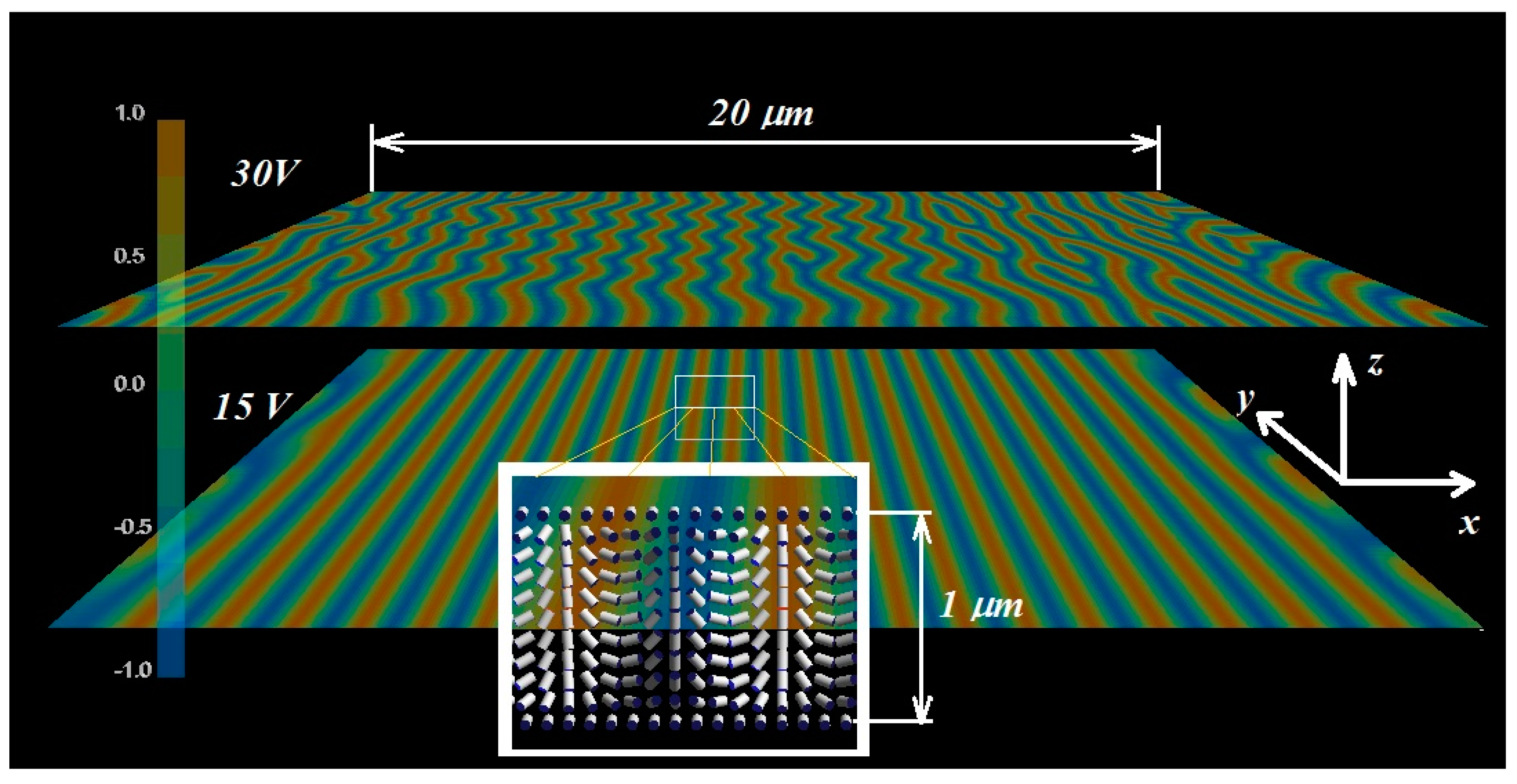
The spatial distribution of the LC director in middle of the layer, which appears as a result of the flexoelectric instability effect, is shown in Figure 2 at voltages of various magnitudes. Note that at zero voltage, the distribution of the LC director is uniform in all three dimensions. In this case, the orientation plane of the director is parallel to the yz-plane and the director’s pretilt angle with respect to the y-axis is 2° (this is a typical value for the pretilt angle achieved in real LC systems). As can be seen, a periodic grating appears in the electric field and the distribution of the director becomes inhomogeneous in both the z- and x-directions. The director rotates around the y-direction as we move along the x-direction. The distance p along the x-direction at which the director makes a full revolution is comparable to the layer thickness. For example, in Figure 3, which shows the distribution for a layer with a thickness of 2 μm, the period p is approximately 1.6 μm. In the center of the layer, the functions describing the x- and z-components of the director are close to sinusoids, with a phase shift of 90° even in a sufficiently strong field (10 V/μm). In this case, the y-component of the director is rather small; that is, the director experiences rotation that is almost in the vertical xz-plane. The sign of the rotation is defined by the sign of the phase shift between curves for nx and nz, which is reversed if we change either direction of the electric field or the sign of the flexoelectric coefficient difference (e1–e3).
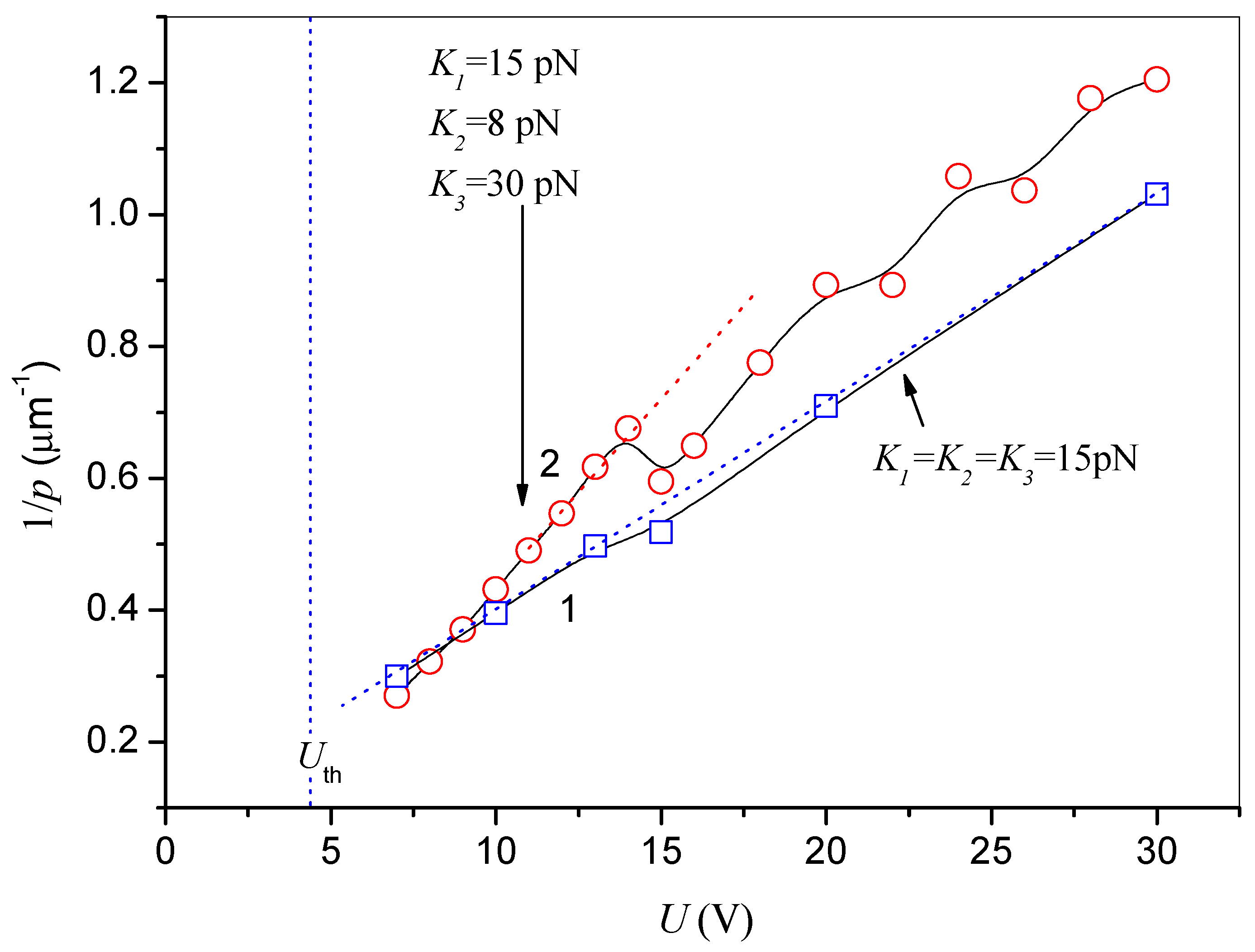
Figure 4 shows the dependence of the spatial frequency (1/p) on the magnitude of the applied voltage. As can be seen, up to very strong fields, when the director in the center of the layer experiences rotation in an almost vertical plane, these dependences are close to the linear; that is, they can be represented in the following form:
where the value of a can be defined as the extrapolation frequency at zero voltage U, when in reality the grating does not exist, since the effect is characterized by the threshold voltage Uth.
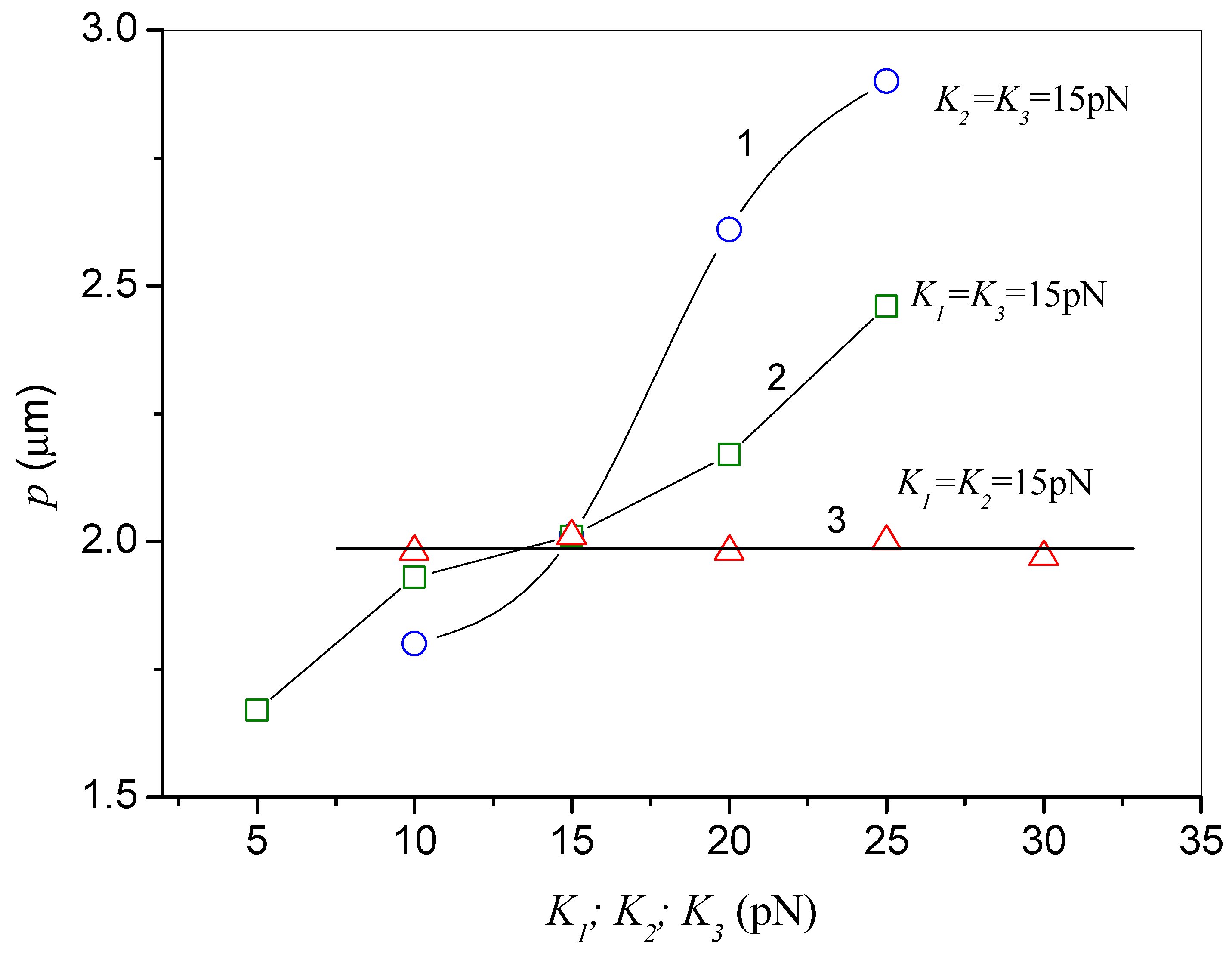
As can be seen in Figure 4, the rate of change in the spatial frequency as the voltage changes is determined by the coefficient b, which in turn depends on the ratio between the elastic constants. As follows from the data in Figure 5, the spatial period depends on the elastic constants K1 and K2, but doesn’t depend on K3. A decrease in K2 leads to an increase in b (compare also curves 1 and 2, Figure 4), and accordingly a greater sensitivity of the spatial frequency to the voltage. In the case of the one-constant approximation, when K1 = K2 = K3 = K, analytical expressions were obtained in [1,2] for both the observed optical period Wth = pth/2 of the induced grating and for the threshold voltage Uth of the appearance of the grating:
where . Since in our case the dielectric anisotropy εa = 0, then μ = 0, and from Equation (5) one can get Wth = d = 2 μm and Uth ≅ 4.5 V, which is in good agreement with the simulations (curve 1, Figure 4).
At sufficiently high electric fields, the calculated value of the spatial frequency oscillates somewhat as the electric voltage U increases (see curve 2 in Figure 4 at U > 15 V). The analysis shows that these oscillations are caused by edge effects associated with the finite size of the modeled domain, which also defines the x-size of the induced grating (in our case, this size is 20 μm in the x-direction, Figure 2). It can also be found that at high voltages, the distribution can become inhomogeneous in the y-direction, as shown in Figure 2 at U = 30 V.
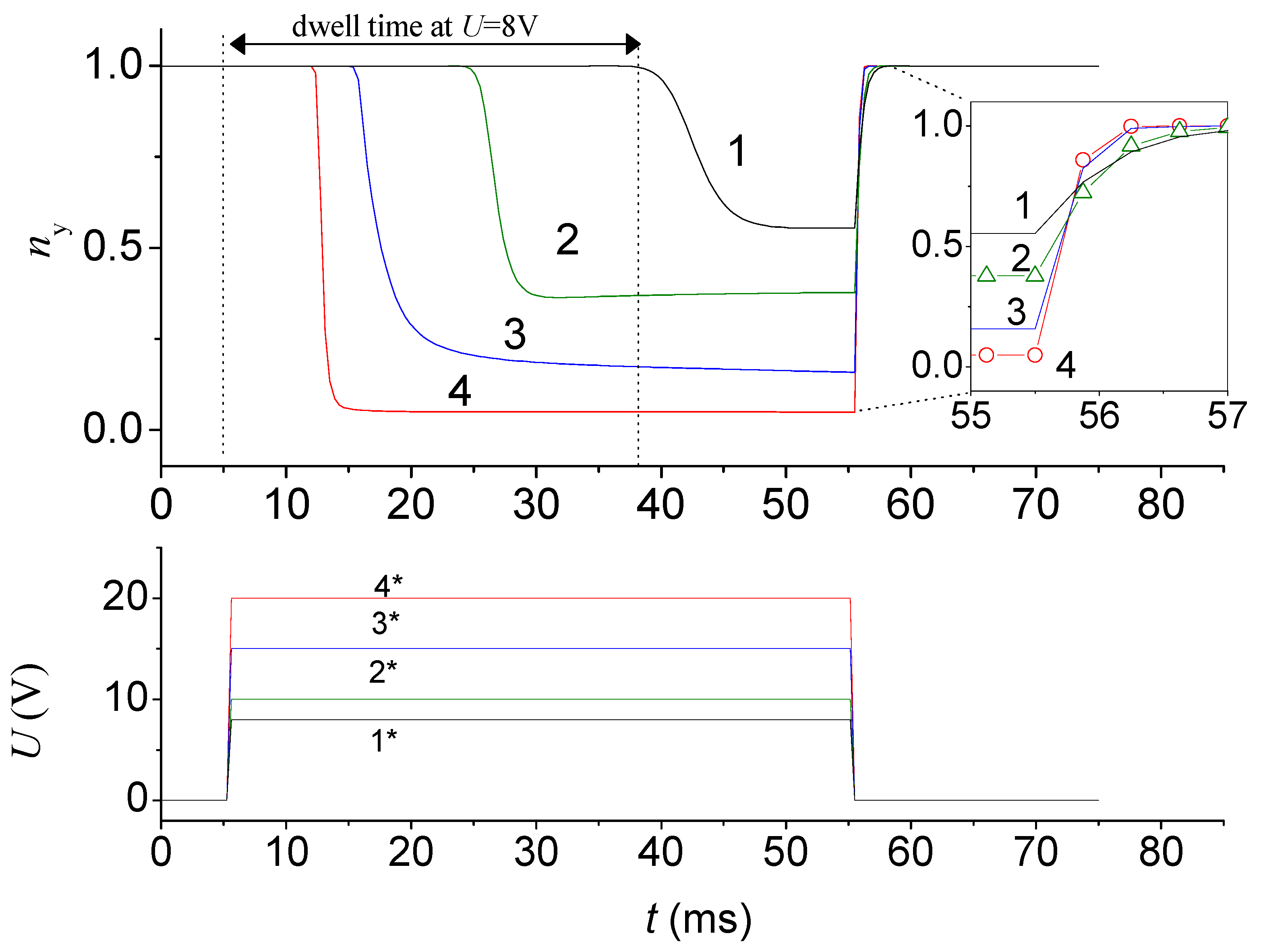
The dependence of the induced grating period on each of the elasticity constants at two other fixed constants is shown in Figure 5. As can be seen, the dependences of the grating period on K1 and K2 are quite pronounced. For example, an increase in K1 from 10 pN to 30 pN leads to an increase in the period by about 1.5 times. It is interesting that the period p does not depend on K3. The dynamics of the appearance and relaxation of the grating at different amplitudes of the voltage pulse is illustrated by the data in Figure 6. These data were obtained for the x-size of the modeled domain Lx = 20 μm, which of course coincides with the size of the induced grating. The analysis shows that the dynamics does not depend on the y-size as long as there are no inhomogeneities in the distribution of the director in the y-direction (I remind that the y-direction is for the field-off alignment). To reduce the computation time, as well as to exclude the influence of inhomogeneities in the y-direction, the data were obtained for a y-size of 100 nm, which in fact corresponds to the two-dimensional case.
Here, the distribution of the director in the y-direction is assumed to be uniform. The analysis also shows that after the application of an electric field, deformation occurs at the edges of the modeled domain and propagates at a certain speed to its center. Therefore, to analyze the time response, a spatial point is chosen in the center of the computational domain in x, y and in the middle of the layer. In this case, the appearance of the grating is accompanied by decreasing the y-component of the director, which changes together with other components but experiences the least oscillations (Figure 3).
Figure 6 shows that the dynamics can be characterized by three characteristic times. First, deformation in the center of the simulated domain begins to appear after a certain dwell time (td). The second time (ton) is for the equilibrium state over the entire computational domain, which includes the time td, and in fact is the time taken to induce an equilibrium grating. After switching off the electric field, very fast relaxation occurs with a characteristic time toff. As can be seen from the inset in Figure 6, this time lies in the sub-millisecond range and decreases as the amplitude of the voltage pulse increases; thus, this time can be associated with the period of the induced grating and can be estimated as:
where K is an effective elastic module and q = 2π/p is the voltage-dependent wavenumber of the induced grating. For example, for K = 15 pN, γ = 0.1 Pa s and p = 2 μm, from (6) we obtain toff ≅ 0.7 ms, which is in good agreement with the numerical data for the lowest voltage in the inset to Figure 6. Note that the relaxation occurs uniformly over the entire simulated domain, with the exception of small near-boundary regions, where the relaxation time is found to be somewhat longer.
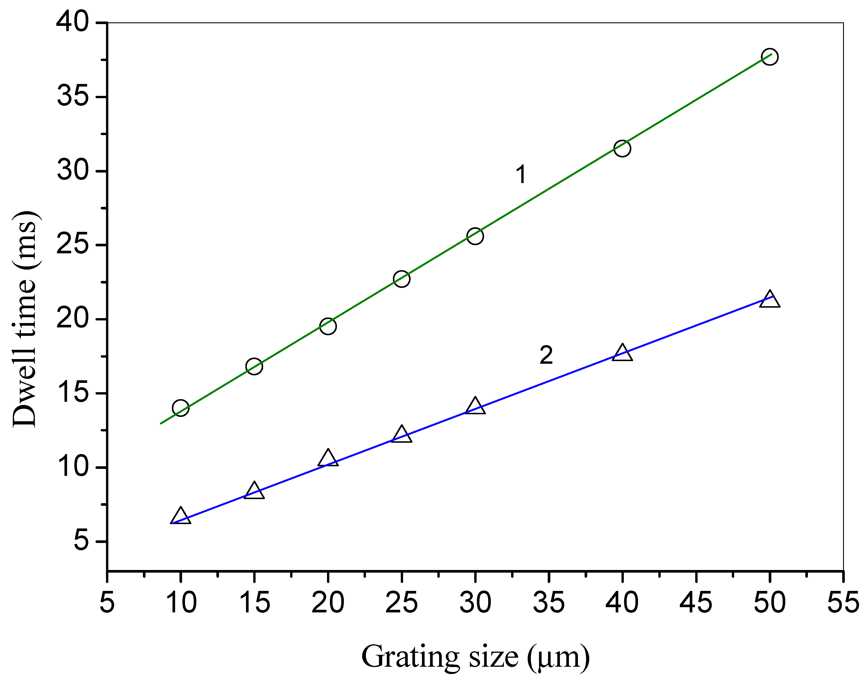
The origin of the dwell time td is well illustrated by the data in Figure 7. As can be seen, the dwell time increases linearly with increases in the size of the simulated domain (the size of the induced grating). This is because the dwell time is due to the propagation time of the deformation from the edges of the simulated domain to its center.
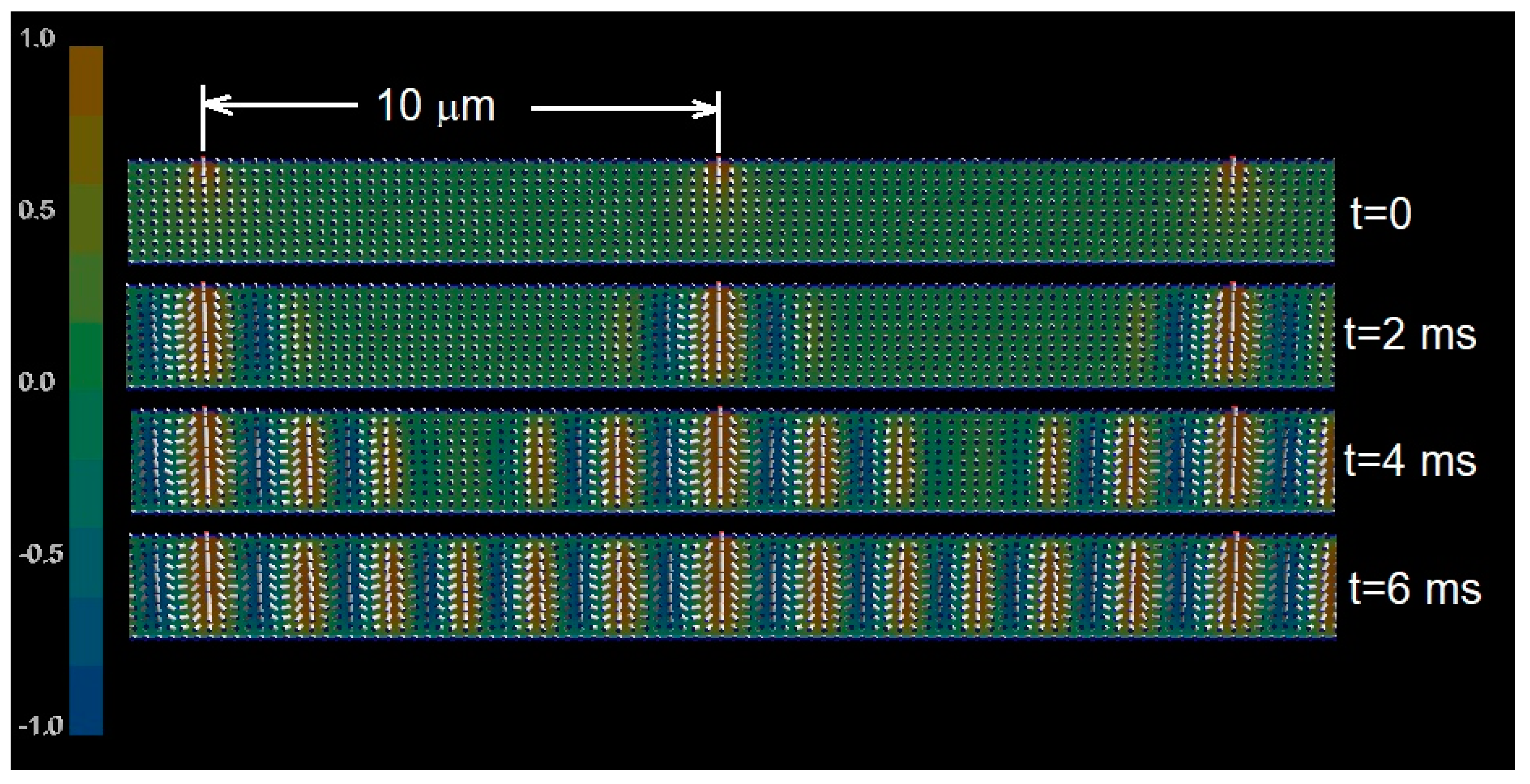
The fact that the time (ton), which includes the dwell time, is determined by its size is very important for understanding the low speed of formation of the periodic texture in the experiments, where static electric fields [3] had to be used. At the same time, understanding the nature of the dwell time allows us to offer a liquid crystal system with a high response speed. Indeed, the boundaries of the modeled domain are, in fact, the region of nucleation of an elastic deformation wave, which propagates to the central part of the simulated domain; therefore, if on the second boundary of the alignment surface, a periodic structure is created from artificial anchoring “defects”, where the conditions for the vertical alignment of the LC director are achieved at short intervals (Figure 8, t = 0), then as a result we can obtain a system for which the total time ton of the grating induction is determined not by its total size, but the period of modulation of the anchoring conditions. In the example in Figure 8, the anchoring modulation period at the upper boundary of the LC layer is 10 μm and the corresponding time ton is about 6 ms, regardless of the overall grating size. Experimentally, the modulation of the anchoring boundary conditions can be carried out using a local focused ion beam treatment [27] of a rubbed polyimide film, which is usually used for the LC alignment.
2.2. Photonic Properties (FDTD Simulations)
The FDTD method is widely used in modern optical simulations. It is based on a direct solution for the Maxwell equations in the time domain. The basics of the FDTD method are described in numerous sources. I would like to recommend the EMPossible site [32], where one can find quite detailed and useful lectures explaining different aspects of the method and possible numerical implementations, which can be a good starting point for developing complicated software.
The author’s FDTDK software module used in this work is directly bound to the LC texture module LCDTDK and is briefly described in [28]. The dielectric properties of materials in FDTDK are defined in terms of the spatial distribution of the dielectric tensor components and by considering their spectral dispersion. The spectral dispersion is considered within framework of the popular, multiple-oscillator Lorentz–Drude model.
It is important to say that in the current study, the spectral dispersion is not taken into account. The virtual LC material is described by frequency-independent values of the principal components of the dielectric tensor (ε|| = 3.06, ε⊥ = 2.31). The last values of the dielectric tensor components correspond to the principal refractive indices n|| = 1.75 and n⊥ = 1.52, which are close to typical for many LC materials (for example, the E7-LC from Merck).
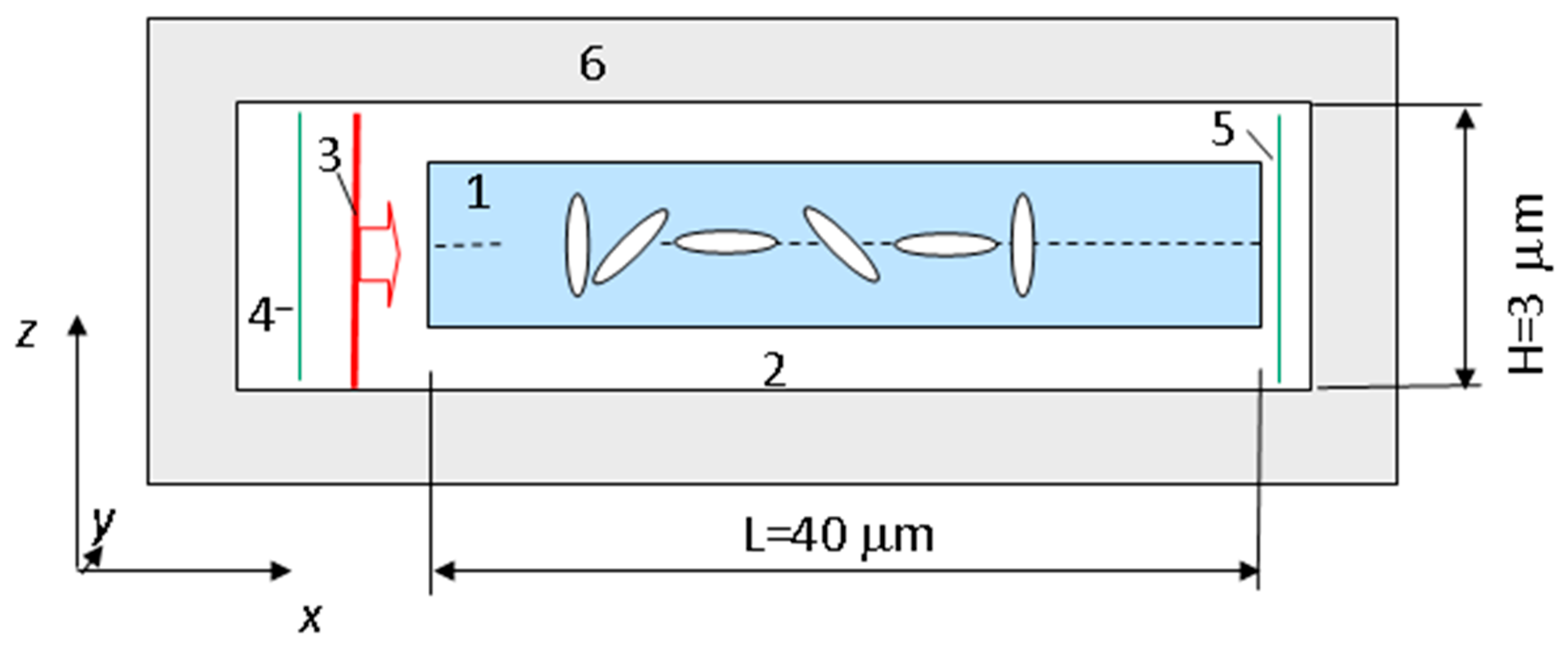
The scheme of the FDTD-simulated space domain is shown in Figure 9. Because the LC layer is homogeneous along the y-axis, all of the d/dy derivatives vanish and the optical problem is reduced to the 2D problem in the xz-plane, which allows for significant increases in efficiency of the FDTD simulations. The LC-layer (1) with a thickness of 2 μm and a length L of 40 μm is placed in a virtual medium (2), with a refractive index of 1.46. Because all principal refractive indices of the LC are higher, the last one allows for a waveguiding regime for the light impinged into the LC layer from the unidirectional light source (3). The virtual sensor (4) is placed in the shadow of the light source (3) and registers only the light reflected by the DLH layer, while the sensor (5) is for the transmitted light. The electrodes used to apply the voltage are neglected in the sense that their refractive indices are set to be the same as for the medium (2). The uniaxial perfectly matched layers (6) prevent reflections from boundaries of the calculated space domain.
The light source (4) generates a pulse of the electromagnetic field propagating along the x-axis. The light has linear polarization in the yz-plane at 45o with respect to the y-axis; thus, both TM- and TE-polarized modes are excited in the LC layer. The magnitude of the pulse is constant in the z-direction. The pulse represents a sine wave (λ = 550 nm) modulated by the Gaussian waveform with a 1/e-height duration of ~1 fs. This results in a rather wide spectrum of generated light, which allows for calculations of the reflectance spectra in a wavelength range of 500 to 4000 nm. The sensor (4) registers across time the components of the electromagnetic field. To obtain the reflectance and transmittance spectra, the ratio of the energy flux in the x-direction (Px) of the electromagnetic field at sensors (4) and (5) to the energy flux irradiated by light source (Pls) is calculated. The values Px and Pls are calculated versus the wavelength by taking the Fourier transform of the field registered by the sensors and finding x-components of the Poynting vector at the sensors and light source (3) positions. Because the x-components of the Poynting vector for the reflected light are negative, the reflectance magnitudes in spectra shown below are also negative. The spectral resolution in the calculated spectra is defined by total registration time for the electromagnetic field. In our calculations, the total registration time is about 2000 fs, which corresponds to resolutions better than 1 nm in the visible spectral range and a few nanometers in the near-infrared range.
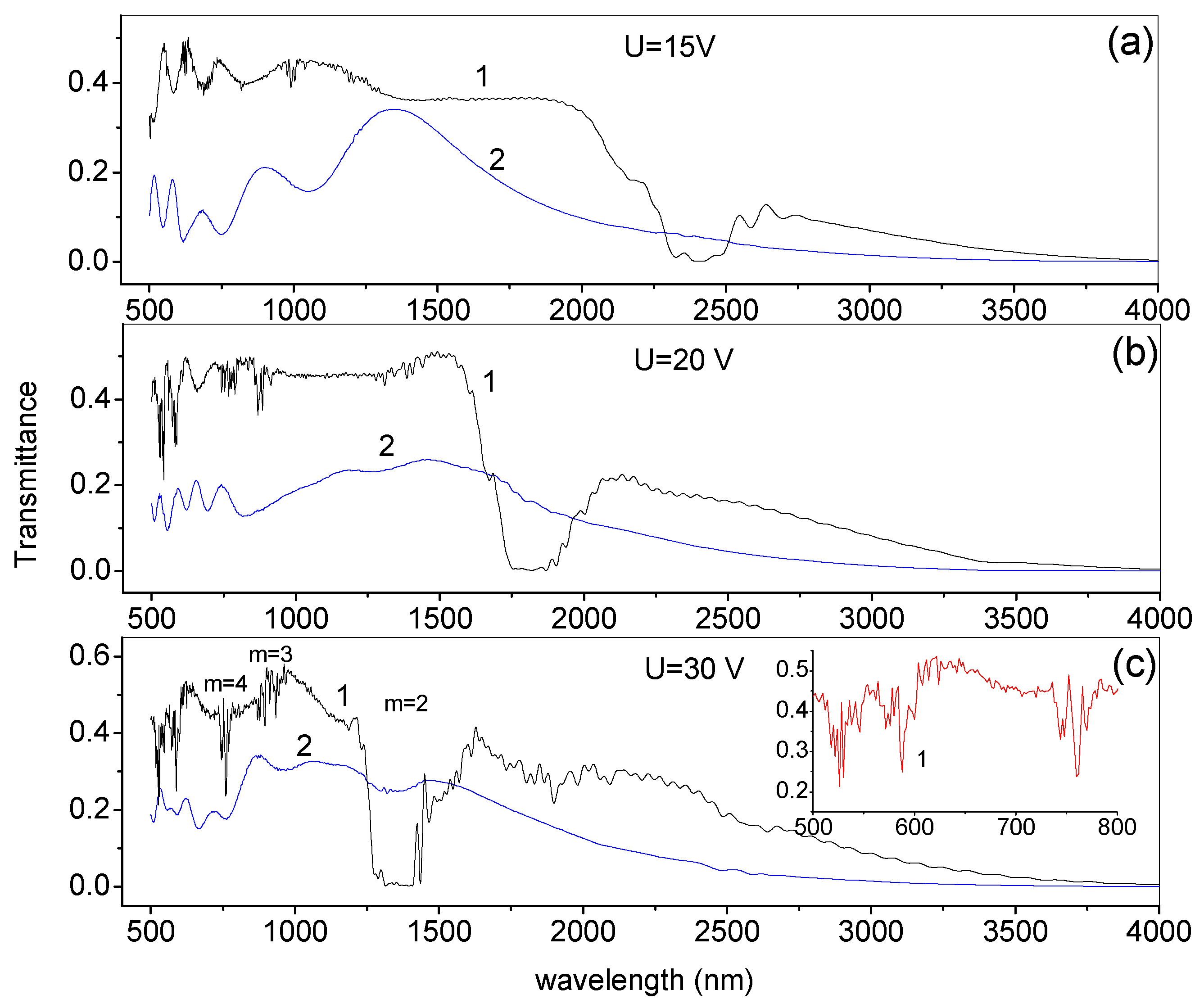
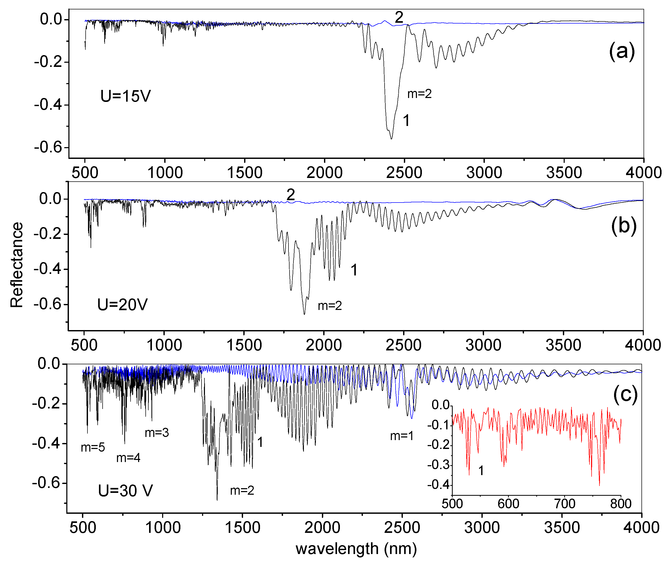
The transmittance and reflectance spectra for z- and y-polarized modes are shown in Figure 10 and Figure 11. The spectra show pronounced photonic stop bands in the wave intervals of 2200–2700, 1700–2200 and 1200–1600 nm for the applied voltages of 15, 20 and 30 V, respectively. The edge positions (λ1, λ2) of these stop bands can be estimated from the Bragg law equation:
where n⊥ and n|| are principal refractive indices of the LC material for the diffraction order m = 2. Actually, at m = 2, exactly the same situation occurs as in the cholesteric liquid crystals. Nevertheless, there is a principal difference from the cholesteric LCs, which is connected to the tilt of the director in the yz-plane when the director rotates around the y-axis (Figure 3). Because of the tilt, the director state with the maximum positive value of the nz director component is not equivalent to the state with the minimal negative nz component. The last property results in that the Bragg reflection is allowed not only for m = 2, but also for m = 1. Moreover, the reflections of the higher orders (m = 3, 4, 5) are very visible, especially in the reflectance spectra at the highest voltage (Figure 11c).
Photonic stop bands are characteristic only for z-polarized light. This is due to the peculiarities of modulation of the LC director field, when it is the director projection onto the xz-plane that undergoes rotation, while the y-component experiences only insignificant oscillations (Figure 3). The reflection spectra clearly show not only stop bands associated with modulation of the LC director field, but also fine oscillations caused by the Fabry–Perot effect, showing interference of reflections from the boundaries of a waveguide with a length of 40 μm. These subtle oscillations are present in both the spectra of z-polarized light and y-polarized light; however, aside from the Fabry–Perot effect, it is easy to see in the reflection spectra of z-polarized light that the photonic stop bands are split into several sub-bands. It can be assumed that the nature of this splitting is the same as in the case of a deformed helix in cholesteric LCs [27,28]. A sufficiently high reflection in the region of higher-order stop bands (m = 4, 5; see insets in Figure 10c and Figure 11c) makes it possible to use them to excite a laser effect in the visible region of the spectrum in the range of 500–800 nm, as was implemented in [27].
Finally, one cannot fail to note the extremely wide spectral range of electric tuning for the positions of the stop bands, which for layers with a thickness of one to two microns, can cover both the near-IR and visible ranges.
3. Conclusions
In this work, we have studied the dynamic properties of the effect of flexoelectric instability, which manifests itself in the induction of a periodic structure (grating) in an electric field. It has been shown that under ideal conditions, the characteristic time of formation of a spatially limited grating is determined by the amplitude of the electric voltage and the size of the grating itself. The latter is associated with the time required for the propagation of elastic deformation from the edges of the grating, where the instability manifests itself most clearly, to its center. It was shown that in the case of a large grating, the time taken for its formation can be drastically reduced through pulsed spatial modulation of the LC anchoring on one of the alignment surfaces, where against the background of uniform planar anchoring conditions, narrow regions are created for the vertical alignment of the LC. In this case, the time of formation for the grating is determined by the period of spatial modulation of the anchoring. The author believes that a similar effect can be obtained by patterning the electrode system at one of the boundaries of the LC layer and using an inhomogeneous electric field; thus, new possibilities are opening up for experimental study and for applying the effects of flexoelectric instability associated with its dynamic properties in pulsed electric fields.
Due to the possibility of rapidly changing the grating period across a wide dynamic range using an external voltage, flexoelectric periodic structures become unique representatives of controlled photonic LCs. In particular, it was shown in this work that in an LC layer with a small thickness (1–2 μm), the spectral position of the induced photonic stop bands can be controlled in the range of hundreds and thousands of nanometers in the visible and near-IR ranges. In the waveguide mode, the Bragg reflection from the periodic structure of the grating is characterized by many orders, which can be used both for creating planar spectral filters and for other photonic devices, such as to obtain laser effects in various spectral ranges.
Funding
This work is supported by the Ministry of Science and Higher Education within a state assignment.
Acknowledgments
I am grateful to my colleagues from the Liquid Crystal Laboratory and Theoretical Department for many useful discussions.
Conflicts of Interest
The author declares no conflict of interest.
References
- Bobylev, Y.P.; Pikin, S.A. Threshold piezoelectric instability in a liquid crystal. Sov. Phys. JETP 1977, 72, 369. [Google Scholar]
- Pikin, S.A. Structural Transformations in Liquid Crystal; Gordon and Breach: New York, NY, USA, 1991. [Google Scholar]
- Barnik, M.I.; Blinov, L.M.; Trufanov, A.N.; Umanski, B.A. Flexoelectric domains in nematic liquid crystals. Sov. Phys. JETP 1977, 73, 1936–1943. [Google Scholar]
- Barnik, M.I.; Blinov, L.M.; Trufanov, A.N.; Umanski, B.A. Flexo-electric domains in liquid crystals. J. Phys. 1978, 39, 417–422. [Google Scholar] [CrossRef] [Green Version]
- Umansky, B.A.; Chigrinov, V.G.; Blinov, L.M.; Podyachev, Y.B. Flexoelectric effect in liquid crystal twisted structures. Sov. Phys. JETP 1981, 81, 1307–1317. [Google Scholar]
- Vistin, L.K. A new electrosructural phenomenon in liquid crystals of nematic type. Dokl. Akad. Nauk SSSR 1970, 194, 1318–1321. [Google Scholar]
- Williams, R. Domains in liquid crystals. J. Chem. Phys. 1963, 39, 384. [Google Scholar] [CrossRef]
- Delev, V.A.; Skaldin, O.A. Electrooptics of hybrid aligned nematics in the regime of flexoelectric instability. Tech. Phys. Lett. 2004, 30, 679–681. [Google Scholar] [CrossRef]
- Palto, S.P.; Mottram, N.J.; Osipov, M.A. Flexoelectric instability and a spontaneous chiral-symmetry breaking in a nematic liquid crystal cell with asymmetric boundary conditions. Phys. Rev. E 2007, 75, 061707. [Google Scholar] [CrossRef]
- Marinov, Y.G.; Hinov, H.P. On the threshold characteristics of the flexoelectric domains arising in a homogeneous electric field: The case of anisotropic elasticity. Eur. Phys. J. E 2010, 31, 179–189. [Google Scholar] [CrossRef] [PubMed]
- Krekhov, A.; Pesch, W.; Buka, A. Flexoelectricity and pattern formation in nematic liquid crystals. Phys. Rev. E 2011, 83, 051706. [Google Scholar] [CrossRef] [PubMed] [Green Version]
- Hinov, H.P. On the Coexistence of the Flexo-Dielectric Walls–Flexoelectric Domains for the Nematic MBBA—A New Estimation of the Modulus of the Difference between the Flexoelectric Coefficients of Splay and Bend |e1z−e3x|. Mol. Cryst. Liq. Cryst. 2010, 524, 26–35. [Google Scholar] [CrossRef]
- Delev, V.A.; Skaldin, O.A.; Timirov, Y.I. The method for determination of flexoelectric coefficients of nematic liquid crystals. Proc. Mavlyutov Inst. Mech. 2017, 12, 101–108. (In Russian) [Google Scholar] [CrossRef] [Green Version]
- Dolganov, P.V.; Ksyonz, G.S.; Dmitrienko, V.E.; Dolganov, V.K. Description of optical properties of cholesteric photonic liquid crystals based on Maxwell equations and Kramers-Kronig relations. Phys. Rev. E 2013, 87, 032506. [Google Scholar] [CrossRef]
- Belyakov, V.A. From liquid crystals localized modes to localized modes in photonic crystals. J. Lasers Opt. Photonics 2017, 4, 153. [Google Scholar]
- Belyakov, V.A.; Semenov, S.V. Localized conical edge modes of higher orders in photonic liquid crystals. Crystals 2019, 9, 542. [Google Scholar] [CrossRef] [Green Version]
- Vetrov, S.Y.; Timofeev, I.V.; Shabanov, V.F. Localized modes in chiral photonic structures. Phys. Uspekhi 2020, 63, 33–56. [Google Scholar] [CrossRef]
- Nys, I.; Beeckman, J.; Neyts, K. Voltage-controlled formation of short pitch chiral liquid crystal structures based on high resolution surface topography. Opt. Expr. 2019, 2, 11492–11502. [Google Scholar] [CrossRef] [PubMed]
- Ahn, S.; Ko, M.O.; Kim, J.H.; Chen, Z.; Jeon, M.Y. Characterization of Second-Order Reflection Bands from a Cholesteric Liquid Crystal Cell Based on a Wavelength-Swept Laser. Sensors 2020, 20, 4643. [Google Scholar] [CrossRef] [PubMed]
- Il’chishin, I.P.; Tikhonov, E.A.; Shpak, M.T.; Doroshkin, A.A. Stimulated emission lasing by organic dyes in a nematic liquid crystal. JETP Lett. 1976, 24, 303–306. [Google Scholar]
- Kopp, V.I.; Zhang, Z.Q.; Genacka, A.Z. Lasing in chiral photonic structures. Prog. Quantum. Electron. 2003, 27, 369–416. [Google Scholar] [CrossRef]
- Coles, H.; Morris, S. Liquid-Crystal lasers. Nat. Photonics 2010, 4, 676–685. [Google Scholar] [CrossRef]
- Inoue, Y.; Yoshida, H.; Inoue, K.; Fujii, A.; Ozaki, M. Improved lasing threshold of cholesteric liquid crystal lasers with in-plane helix alignment. Appl. Phys. Express 2010, 3, 102702. [Google Scholar] [CrossRef]
- Xiang, J.; Varanytsia, A.; Minkowski, F.; Paterson, D.A.; Storey, J.M.D.; Imrie, C.T.; Lavrentovich, O.D.; Palffy-Muhoray, P. Electrically tunable laser based on oblique heliconical cholesteric liquid crystal. Proc. Natl. Acad. Sci. USA 2016, 113, 12925–12928. [Google Scholar] [CrossRef] [PubMed] [Green Version]
- Ortega, J.; Folcia, C.L.; Etxebarria, J. Upgrading the Performance of Cholesteric Liquid Crystal Lasers: Improvement Margins and Limitations. Materials 2018, 11, 5. [Google Scholar] [CrossRef] [Green Version]
- Brown, C.M.; Dickinson, D.K.E.; Hands, P.J.W. Diode pumping of liquid crystal lasers. Opt. Laser Technol. 2021, 140, 107080. [Google Scholar] [CrossRef]
- Shtykov, N.M.; Palto, S.P.; Geivandov, A.R.; Umanskii, B.A.; Simdyankin, I.V.; Rybakov, D.O.; Artemov, V.V.; Gorkunov, M.V. Lasing in liquid crystal systems with a deformed lying helix. Opt. Lett. 2020, 45, 4328–4331. [Google Scholar] [CrossRef]
- Palto, S.P. The Field-Induced Stop-Bands and Lasing Modes in CLC Layers with Deformed Lying Helix. Crystals 2019, 9, 469. [Google Scholar] [CrossRef] [Green Version]
- Blinov, L.M.; Palto, S.P. Cholesteric Helix: Topological Problem, Photonics and Electro-optics. Liq. Cryst. 2009, 36, 1037–1047. [Google Scholar] [CrossRef]
- Palto, S.P.; Barnik, M.I.; Geivandov, A.R.; Kasyanova, I.V.; Palto, V.S. Spectral and polarization structure of field-induced photonic bands in cholesteric liquid crystals. Phys. Rev. E 2015, 92, 032502. [Google Scholar] [CrossRef] [PubMed]
- Peng, F.; Huang, Y.; Gou, F.; Hu, M.; Li, J.; An, Z.; Wu, S.-T. High performance liquid crystals for vehicle displays. Opt. Mat. Express 2016, 6, 717–726. [Google Scholar] [CrossRef]
- Rumpf, R.C. Electromagnetic Analysis Using Finite-Difference Time-Domain; EMPossible: El Paso, TX, USA; Available online: https://empossible.net/academics/emp5304/ (accessed on 28 June 2021).
Figure 1.
Schematic illustration of the LC director distribution for different domains: Williams domains (a); flexoelectric domains (b). For the Williams domains, the initial alignment is along the x-axis, while for the flexoelectric domains the alignment is along the y-axis.
Figure 1.
Schematic illustration of the LC director distribution for different domains: Williams domains (a); flexoelectric domains (b). For the Williams domains, the initial alignment is along the x-axis, while for the flexoelectric domains the alignment is along the y-axis.

Figure 2.
In-plane director distribution in the middle (z = 0.5 μm) of the LC layer at voltages of 15 V (bottom plane) and 30 V (top plane) applied across the LC layer of a thickness of one micrometer. The color scale is for the z-component of the LC director. The inset shows the director distribution in the xz-plane for a fraction of the calculation domain in the middle at 15 V.

Figure 3.
Director distribution in the center of a 2-μm-thick layer at a voltage of 20 V after switching on an electric voltage with an amplitude of 20 V.
Figure 3.
Director distribution in the center of a 2-μm-thick layer at a voltage of 20 V after switching on an electric voltage with an amplitude of 20 V.

Figure 4.
Dependence of the spatial frequency (1/p) of the induced grating on the applied voltage for two series of elastic coefficients: (1) K1 = K2 = K3 = 15 pN; (2) K1 = 15 pN, K2 = 8 pN, K3 = 30 pN. The thickness of the LC layer d = 2 μm.
Figure 4.
Dependence of the spatial frequency (1/p) of the induced grating on the applied voltage for two series of elastic coefficients: (1) K1 = K2 = K3 = 15 pN; (2) K1 = 15 pN, K2 = 8 pN, K3 = 30 pN. The thickness of the LC layer d = 2 μm.

Figure 5.
Dependence of the spatial period p on one of the three elastic coefficients at fixed and equal values of the other two elastic coefficients for U = 13 V.
Figure 5.
Dependence of the spatial period p on one of the three elastic coefficients at fixed and equal values of the other two elastic coefficients for U = 13 V.

Figure 6.
Dynamic response of the director state (ny-component, top) to the applied voltage pulse (bottom).
Figure 6.
Dynamic response of the director state (ny-component, top) to the applied voltage pulse (bottom).

Figure 7.
Dependence of the dwell time on the x-size of the calculate domain (grating size): 1 − U = 10V; 2 − U = 15 V.
Figure 7.
Dependence of the dwell time on the x-size of the calculate domain (grating size): 1 − U = 10V; 2 − U = 15 V.

Figure 8.
Dynamics of the grating induction in case of the modulated (planar–vertical) anchoring at the top alignment surface. The anchoring is modulated by the pulse function, with a period of 10 μm and pulse width of 0.4 μm defining the vertical alignment. The layer thickness is 2 μm and the driving voltage is 15 V. The color scale is for the z-component of the LC director.

Figure 9.
Scheme of the FDTD simulated domain. (1) LC grating layer; (2) the medium with a refractive index of 1.46; (3) unidirectional light source; (4) sensor for the reflected light; (5) sensor for the transmitted light; (6) the uniaxial perfectly matched layers.
Figure 9.
Scheme of the FDTD simulated domain. (1) LC grating layer; (2) the medium with a refractive index of 1.46; (3) unidirectional light source; (4) sensor for the reflected light; (5) sensor for the transmitted light; (6) the uniaxial perfectly matched layers.

Figure 10.
(a–c) Transmittance spectra for the z- (1) and y-polarized (2) components of the light at different voltages U. The inset in (c) shows a fraction of the same spectrum in visible range with a higher spectral resolution.
Figure 10.
(a–c) Transmittance spectra for the z- (1) and y-polarized (2) components of the light at different voltages U. The inset in (c) shows a fraction of the same spectrum in visible range with a higher spectral resolution.

Figure 11.
(a–c) Reflectance spectra for the z- (1) and y-polarized (2) components of the light at different voltages U. The inset in (c) shows a fraction of the same spectrum in visible range with a higher spectral resolution.
Figure 11.
(a–c) Reflectance spectra for the z- (1) and y-polarized (2) components of the light at different voltages U. The inset in (c) shows a fraction of the same spectrum in visible range with a higher spectral resolution.

Publisher’s Note: MDPI stays neutral with regard to jurisdictional claims in published maps and institutional affiliations. |
© 2021 by the author. Licensee MDPI, Basel, Switzerland. This article is an open access article distributed under the terms and conditions of the Creative Commons Attribution (CC BY) license (https://creativecommons.org/licenses/by/4.0/).
Share and Cite
MDPI and ACS Style
Palto, S.P. Dynamic and Photonic Properties of Field-Induced Gratings in Flexoelectric LC Layers. Crystals 2021, 11, 894. https://0-doi-org.brum.beds.ac.uk/10.3390/cryst11080894
AMA Style
Palto SP. Dynamic and Photonic Properties of Field-Induced Gratings in Flexoelectric LC Layers. Crystals. 2021; 11(8):894. https://0-doi-org.brum.beds.ac.uk/10.3390/cryst11080894
Chicago/Turabian StylePalto, Serguei P. 2021. "Dynamic and Photonic Properties of Field-Induced Gratings in Flexoelectric LC Layers" Crystals 11, no. 8: 894. https://0-doi-org.brum.beds.ac.uk/10.3390/cryst11080894
Note that from the first issue of 2016, this journal uses article numbers instead of page numbers. See further details here.