Article

The Architectonics Features of Heterostructures for IR Range Detectors Based on Polycrystalline Layers of Lead Chalcogenides

by
Yuliya Mikhailovna Spivak
1,
Irina Evgen’evna Kononova
1,
Pavel Vasil’evich Kononov
2,*,
Vyacheslav Alexeyevich Moshnikov
1 and
Sergey Anatol’evich Ignat’ev
2
1
Department of Micro- and Nanoelectronics, Faculty of Electronics, Saint-Petersburg Electrotechnical University «LETI», 5, pr. Popova, 197376 Saint-Petersburg, Russia
2
Department of Descriptive Geometry and Graphics, Faculty of Basic and Human Sciences, Saint-Petersburg Mining University, 2, 21st Line, 199106 Saint-Petersburg, Russia
*
Author to whom correspondence should be addressed.
Submission received: 15 August 2021 / Revised: 14 September 2021 / Accepted: 15 September 2021 / Published: 19 September 2021
(This article belongs to the Special Issue Hierarchical Composite Materials)

Abstract

:
A model is developed for the formation of porous intragranular architectonics of nanostructured polycrystalline layers of lead chalcogenides for photodetectors and IR emitters. The layers are obtained under the conditions of thermal evaporation in a quasi-closed volume by the “hot wall” method followed by sensitizing heat treatment in an iodine-containing atmosphere. Model concepts are developed considering the experimental results of studying the intragranular structure of lead chalcogenides through original combined AFM methods over the cross-section of porous grains (cores) encapsulated by an oxide shell (lateral force microscopy and local tunneling I–V spectroscopy).

1. Introduction

There is currently a transition taking place in materials science from traditional methods of obtaining layered and film nanostructures [1,2,3,4,5,6,7,8] to active atomic–molecular design and complicated architectonics [9,10,11,12,13], combining designs of several hierarchical [14,15,16,17,18,19,20,21] levels with specific functional properties.
In the last several decades, a research area based on polycrystalline chalcogenides [22,23,24,25,26,27,28,29,30,31,32,33] and their solid solutions for IR photodetectors and emitters [21,22,23,24,25,26] has been successfully developing. The optimization of technological processes is accompanied by the sensitization of materials and the creation of protective oxide shells [28,29,30,31,32] consisting of different chemical compounds, namely PbOx, PbSeO3, bi- and tetra-oxyselenites and oxyselenates (2PbO∙PbSeO3, 4PbO∙PbSeO3) [29]. The photosensitive properties of the layers depend significantly on the composition of the oxide phase.
Lead chalcogenides are narrow-gap semiconductors, the band gap of which is 0.39 eV for lead sulfide PbS, 0.27 eV for lead selenide PbSe and 0.32 eV for lead telluride PbTe [31]. A significant role is played by the value of deviation from stoichiometry: with an excess of lead atoms lead chalcogenide crystals have n-type conductivity; however, with an excess of chalcogen they have p-type conductivity. Effective devices based on nanostructured polycrystalline layers of binary compounds, and solid solutions based on them, can be obtained in the spectral range of 2.5 µm. The advantages of these devices include high operating speeds, small overall and weight parameters, low power consumption, and operation at room temperature [31,33].
The most preferable is an oxidized layer close in composition to PbSeO3, since this phase forms at a certain temperature when oxidizing the stoichiometric composition of PbSe, at which the concentration of free charge carriers is intrinsic, which is important for the high sensitivity of photodetectors [31,34,35].
Combined photodetectors and emitters for optocouplers based on lead chalcogenides must meet the requirements of different values of the band gap [31,36,37]. This is due to the fact that photodetectors must operate by taking into account the Burstein–Moss effect. This effect describes the shift of the edge of the intrinsic absorption region of the semiconductor towards higher frequencies with an increase in the concentration of conduction electrons, and their filling of the conduction band. In narrow-gap materials, the role of the Burstein–Moss shift can become noticeable, and therefore semiconductor layers with a higher value of the band gap are used for IR emitters.
To increase the band gap, a solid solution with the addition of a binary compound (usually CdSe) is used [35,38,39]. Among other features, it is required to control the formation of the oxide shell. Its composition depends on the type and concentration of impurities in the grain. It is also necessary to ensure the doping of the grains with oxygen [3,18,32]. Oxygen will act as an acceptor impurity and change the conductivity type of the grains. This task becomes more difficult in practice due to the blockage of oxygen diffusion with an increase in the thickness of the growing oxide shell.
Due to the difference in the diffusion coefficients of the initial components through the oxide shell (the release of Pb, Se, Cd from the core to the outside of the grain and oxygen through the shell to the inside of the core), the oxide layer grows outside, and voids appear in the intragranular space (Cabrera–Mott law).
To ensure the possibility of controlling the penetration of oxygen into the shell, it is effective to use the addition of iodine vapor. This process provides the formation of highly volatile compounds PbI2, CdI2 and others, and thus does not allow for reaching thicknesses of the oxide shell that negatively affect the possibility of oxygen diffusion inside. On the other hand, the release of the main elements from the lead chalcogenide core and solid solutions based on them through the oxide shell should lead to the formation of voids in the core space (grains nanostructuring). Lead and cadmium iodides could also be used to design the porous intragranular space.
It should be noted that the architectonics [9,10,11,14,15,16,17,19] of the intergranular structure for photodetectors and emitters differs significantly.
In photodetectors, a layer of photosensitive material with an inverted conductivity type should form under the oxide shell. There must be a percolation channel for the current flowing through the areas with inverted conductivity types of the intragranular space. The concentration of charge carriers in the inverted p-type layer should be close to the value of the intrinsic concentration of charge carriers in order for the change in the conductivity of this percolation layer to be more effective, due to excess holes injected into the p-channel under illumination from n-type regions of the grain. In this case, the crystal quality of grain structuring should be very high. It is also required to block the n-regions of the intergranular space with p-type interlayers or voids to interrupt the current flow through the n-type shunt cluster.
For photoluminescence emitters, it is not necessary to provide a percolation conductive channel. However, a high crystalline perfection is required to provide effective photoluminescence.
This article is somehow a summing up and generalization of research results in the field of nanostructured polycrystalline layers of lead chalcogenides for the development photodetectors and mid-IR emitters, provided under the supervision of the Head of Laboratory of Nanomaterials, SPbETU “LETI”, Professor V.A. Moshnikov. The aim of this work is to summarize research in several of our published works, and to develop a new model of formation processes for porous intragranular architectonics [9,10,11] of photodetectors and IR emitters based on nanostructured polycrystalline lead chalcogenide layers, obtained under conditions of thermal evaporation in a quasi-closed volume by the “hot wall” method.

2. Materials and Methods

2.1. Synthesis of Polycrystalline Layers of Lead Chalcogenides

Polycrystalline layers were obtained via several technological stages: the substrate treatment; the charge synthesis; n-type obtainment of PbSe layers and activation annealing.
Cover glass from the “Druzhnaya Gorka” factory S-29 (GOST 6672-53 (GOST—Russian state standard)) was used as substrate. Firstly, glass substrates were chemically treated in a special solution based on hydrofluoric acid, using stirring techniques in order to obtain the required matrix of defects on their surface. Hydrofluoric acid at 45% solution was used for etching (chemically pure substance, GOST 10484-78).
The charge was synthesized by fusing the components in quartz ampoules at a temperature above the melting point of PbSe. Pure components (Pb, Se, Cd) were used for the synthesis of the charge: Pb (Granular lead C1, GOST 3778-98), Se (high purity selenium, granules, 22-4, TU 6-09-2521-77), Cd (Granular cadmium, TU 6-09-5434-88), extra pure iodine and CAS: 7553-56-2. The initial charge was either crushed lead selenide or doped solid solution of lead selenide: cadmium selenide. Pre-synthesized PbI2 was used as a ligature.
To provide the required position of maximum on the spectral characteristic, Cd was used as dopant and a Pb1−xCdxSe solid solution (x = 0..0.2 mol) was formed. This led to an increase in the band gap and shifted the spectral characteristic to shorter wavelengths. The synthesis temperature exceeded the melting point of lead selenide by 20 ℃. The ampoule was kept at 1100 ℃ for 2 h to achieve homogenization of the liquid phase. After that, the ampoule was quenched in cold water. To achieve a high homogeneity of the charge, we used subsequent annealing at a temperature of 600–700 ℃, corresponding to sublimation during the deposition of films [34,35].
The deposition of polycrystalline PbSe and PbxCd1−xSe layers was carried out by thermal evaporation of the charge in vacuum by the Lopez–Otero method (so-called “hot wall” method) by using the standard vacuum installations UVN 71, USSR [40]. The design of the evaporation chamber used in the implementation of the hot wall method in this work is shown in Figure 1.
The ampoule is made of vacuum compression quartz glass. A molybdenum tape 3 mm wide was used for heating elements. The main and additional sources of steam were powered from independent sources. Equalization of the temperature gradient in both zones was achieved using special metal screens. Temperature control in the zones of the main and additional source was carried out with chromel–alumel thermocouples. The substrate temperature was controlled in the 100–210 °C range with an accuracy of 0.5 °C. The evaporator temperature was varied in the 600–700 °C range. To reduce the effect of radiation from the heating element of the main source on the carousel with substrates, a special system of screens was used. The residual pressure in the system, as a rule, was ≈10−5 Pa.
Heat treatment was carried out in a muffle furnace (SNOL-1,4.2,5.1,2/12.5), in a quasi-closed volume in an atmosphere of oxygen and iodine. The thicknesses and properties of the films were controlled by the composition and weight of the charge, the deposition time, and the temperature of sublimation and condensation. The thickness of the layers, as a rule, was ≈0.8–1 µm.
Saturated aqueous solution of Trilon B (disodium salt of ethylenediamine tetraacetic acid, Solins, CAS # 6381-92-6) was used for etching the oxidized layer.

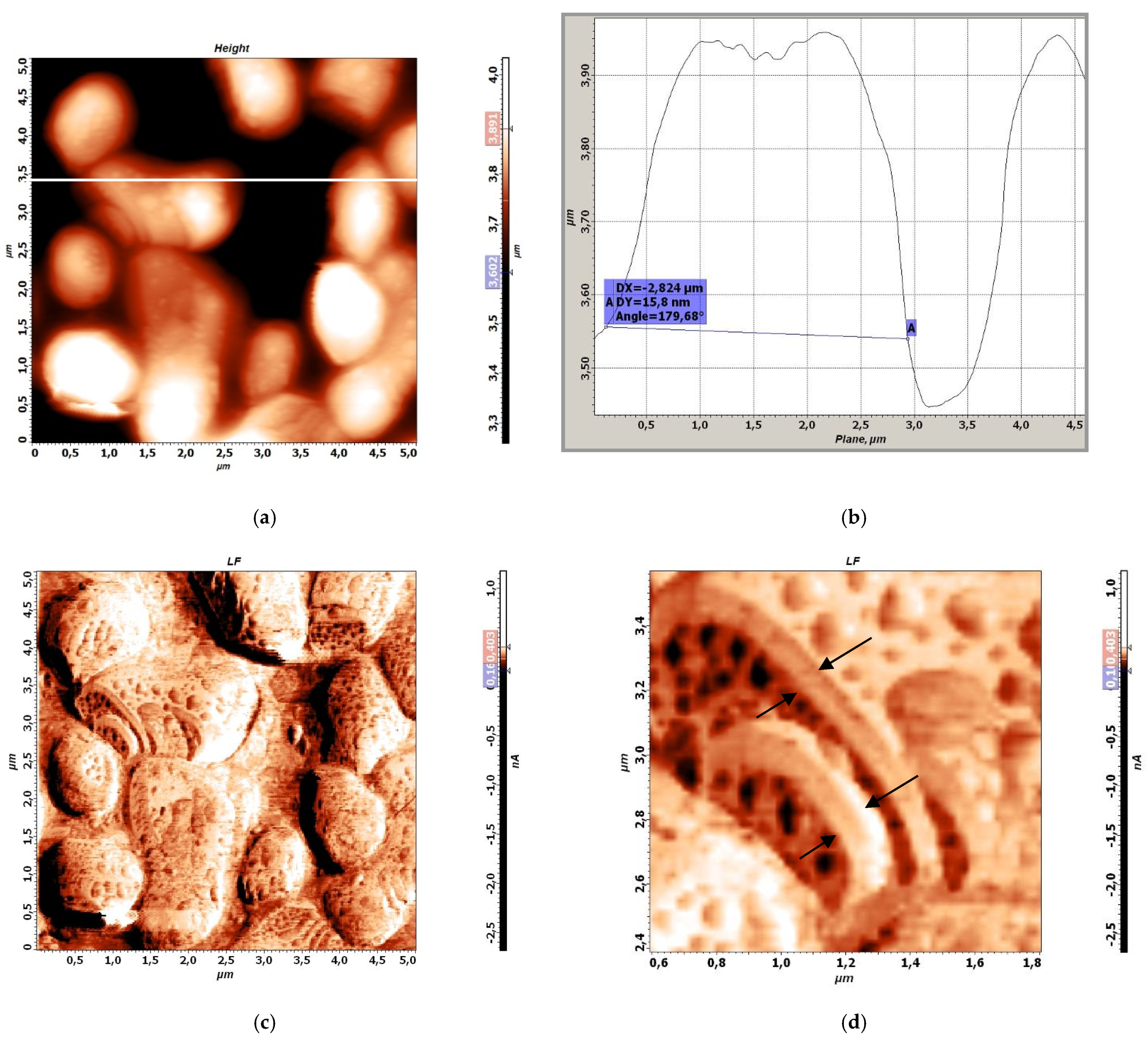
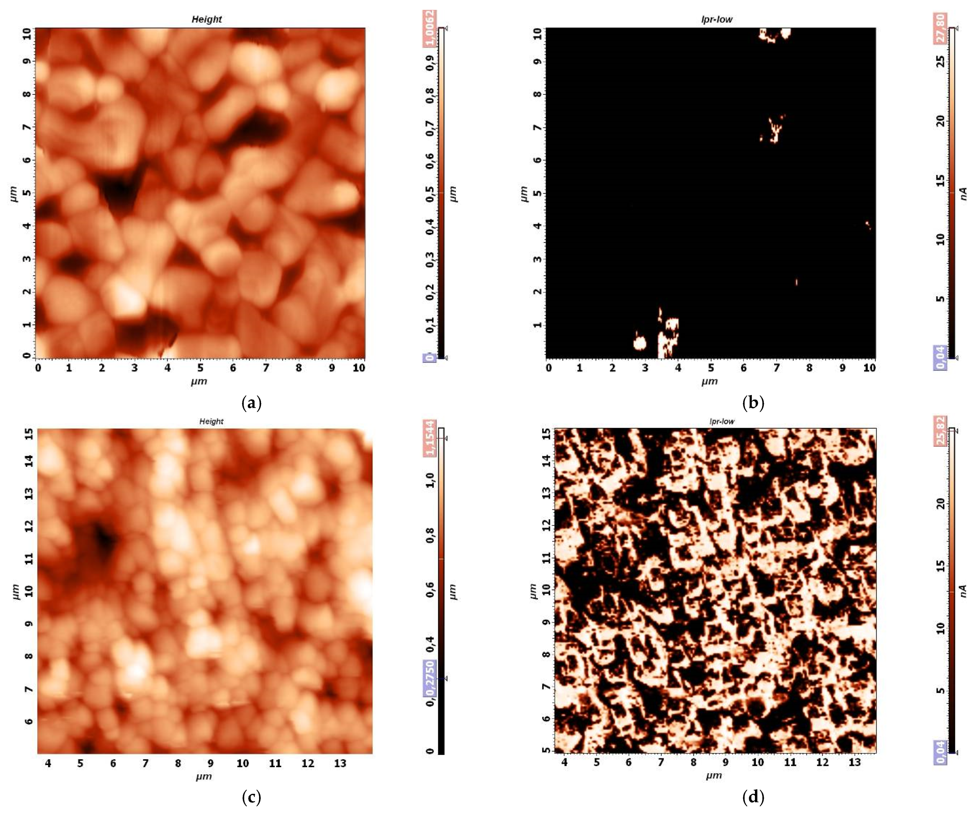
2.2. Application of An Original Combination of AFM Techniques for Providing Cross-Sections of Porous Cores Encapsulated by An Oxide Shell and Its Study

To analyze the structure of the obtained photosensitive layers based on doped PbCdSe solid solutions, force lithography by an AFM probe was used in combination with lateral force microscopy (the value of the torsion cantilever bending as an analytical signal) of the surface and the obtained cross-sections. The studies were carried out using the Ntegra Terma scanning probe microscope (NT-MDT, Zelenograd). AFM probes of CGS01, NSG01 and Pt, TiN or diamond-coated conductive tips were used for the corresponding AFM techniques (contact AFM and lateral force microscopy, plowing lithography, scanning spreading resistance, and local tunnel current spectroscopy). For plowing (force) lithography, more rigid AFM probes were used (NSG01, NSG10); the position of the Set Point was changed, increasing the clamping force by a factor of 4 (SP = 2 at AFM in contact mode, and SP = 8 during force lithography). The reliability and reproducibility of the data was verified by comparing AFM data across several sizes of scanning area, data at forward and backward pass, at different scanning speeds and scan directions, and statistical data accumulation.
Figure 1 shows the data of lateral force microscopy (LFM) when compared with the data of topography images obtained in contact mode. Figure 2a shows an overview of the surface of the photosensitive polycrystalline layer Pb1−xCdxSe <I> (x = 0.18) after the cross-section of several grains by plowing (force) lithography. As one can see from Figure 2a, the sample layer consists of grains with a size of about 0.66..2.5 μm. Where the surface of the grains was developed, nanoprotrusions (specific formations) are observed (Figure 2b). According to the LSM method, such inclusions are also detected (Figure 2c,d). As one can with simultaneous registration with LFM, specific formations on the surface of the grains were found. Such specific formations (diameter ~ 100..200 nm, height ~ 5..10 nm) covered almost the entire surface of the grains with an oxidizing coating. The deviation of the height of these formations was relatively small in comparison with the grain sizes of the polycrystalline layer. Since the roughness within the individual grain was less than 5–6 nm, it is supposed that such formations are products of the release of metals from the grain and an almost formed shell in places where the seepage process is still possible. The formation of oxide in these places leads to the appearance of a system of nano-hills (Figure 2). At the same time, high structural perfection inside the grain is maintained.
We supposed that the dark spots on the grain cross-section (Figure 2d) are possibly voids, so the center of the grains is porous. As noted, part of the metal diffusing from the grain to the surface does not have time to react with iodine. This leads to the formation of small oxide build-ups on the surface of the shell (Figure 2).
Experiments on the mechanical section of grains with an AFM probe made it possible to visualize the shape of the grain surface on the cross-section and to estimate the oxide thickness (≈100…120 nm, by data on Figure 2d, arrows shown on cross-section of the grain). This is important in optimizing the technological conditions when sensitizing annealing. In support of this assumption, the observed light layer on the LFM data of a grain section (edges are indicated by arrows, Figure 2d) suggests the following: (1) the sample under study was previously subjected to sensitizing annealing, in which it is known that an oxide coating is formed [31,33,36], (2) on the data of the LFM, the layer differs in color from the rest of the structure (the color corresponds to the different friction force of the probe on the sample surface according to the bar line on the right in the image), which indicates that the light layer differs in phase composition from the central part of the grain, (3) the light layer evenly covers all the grains that have undergone cross-sectioning by plowing lithography, rather than some individual grains. In addition, the presence of a high ohmic oxide coating is confirmed by the data on scanning microscopy of the spreading resistance (Figure 3). According to Figure 3a,b, one can see that at the applied voltage of ≈2.5 V, most of the surface of the polycrystalline layer becomes conductive, in contrast to the PbCdSe layer, which is covered with an oxide coating that conducts sections (breakdown of the dielectric coating) mainly at U > 5 V (Figure 3c,d). The SSRM method was subsequently used to control the quality of removal of the oxidized coating through chemical etching.
The research results of the change in the type of charge carriers inside the grain depth revealed the presence of an internal p–n junction inside the PbCdSe <I> grain. Methodological features of this approach have been published before [3]. Here, we briefly note that the idea of the methodology was as follows: an AFM probe with a conductive coating (Pt, Au) was positioned on the surface of a very thin (tunnel thin) oxide layer in contact, and local tunneling current spectra were recorded as a function of the applied voltage (LTS). A thin oxidized layer acts as a tunnel vacuum gap in scanning tunnel spectroscopy and in scanning tunnel microscopy (STM). By the nature of the local tunneling spectra, it was possible to carry out a classical analysis for scanning tunneling spectroscopy (to estimate the positions of the edges of the valence and conduction bands, their positions relative to the origin of coordinates, etc.) [27]. The transitions begin when the potential is applied to the tip of the probe when the bottom of the conduction band is reached and above. In this case, it is assumed that practically the entire potential difference falls on the high-resistance vacuum gap. When the potential of the opposite sign is applied—the tunneling of electrons from the valence band—the metal probe will occur when the energy position of the metal probe is reached below the top of the valence band. In narrow-gap materials, as a rule, the Burstein–Moss effect is observed. When charge carriers fill the conduction band, for example, the shift can be commensurate with the value of the band gap. This leads to a shift of the I–V characteristic towards an increase in the potential value by the values of the Burstein–Moss shift (when joining an optocoupler for detectors based on PbSe, as a rule, emitters based on PbCdSe solid solutions are chosen, since CdSe additions lead to an increase in the width of the energy band and to ensure efficient electron tunneling).
The problem of obtaining a tunnel-transparent layer on the surface of semiconductor grains was solved as follows: the oxide coating was removed through chemical etching and the quality of removal was controlled by scanning spreading resistance microscopy; then, the sample was kept in an oxygen atmosphere to form a tunnel-transparent oxide layer. In addition, multistage chemical etching of a semiconductor nanostructure layer of lead chalcogenides with the subsequent growth of a tunnel-transparent oxide layer made it possible, depending on the etching cycle number, to remove part of the material “moving” with a new etching cycle into the grain, and thus, measure the local current spectra from the surface grains at its center. Each stage included the following steps: removal of the oxidized coating by chemical etching, followed by exposure in air to form a tunnel-transparent oxide layer on the sample surface, then measurement of LTS spectra using AFM. Each time (each stage) we carried out such a cycle we moved deeper into the grain, and thus observed the features of the electrophysical properties along the depth of the grain.
In practice, this was achieved in the following way. To study the electrophysical properties at selected points of the formed percolation system, the dielectric oxide coating was removed from the layer surface. For this study, the layers of the PbCdSe solid solution were chemically etched in a saturated Trilon B solution in water for 10–40 min. The removal of the oxide coating was monitored visually (by changing the color of the layer) by using scanning spreading resistance microscopy. The study was carried out by means of the AFM mode using TiN-coated AFM probes with a radius of curvature ~10 nm. In [3], the experimental results of the local analysis of the conductivity of lead chalcogenides inside the grain are shown, obtained using the method of tunneling conductive atomic force microscopy.
It was revealed that the semiconductor layer under the oxide coating formed during sensitizing annealing demonstrates p-type electrical conductivity. In the center of the grain, a gradual change in the type of free charge carriers is observed; the center of the grain retains the n-type of electrical conductivity.

3. Results and Discussion

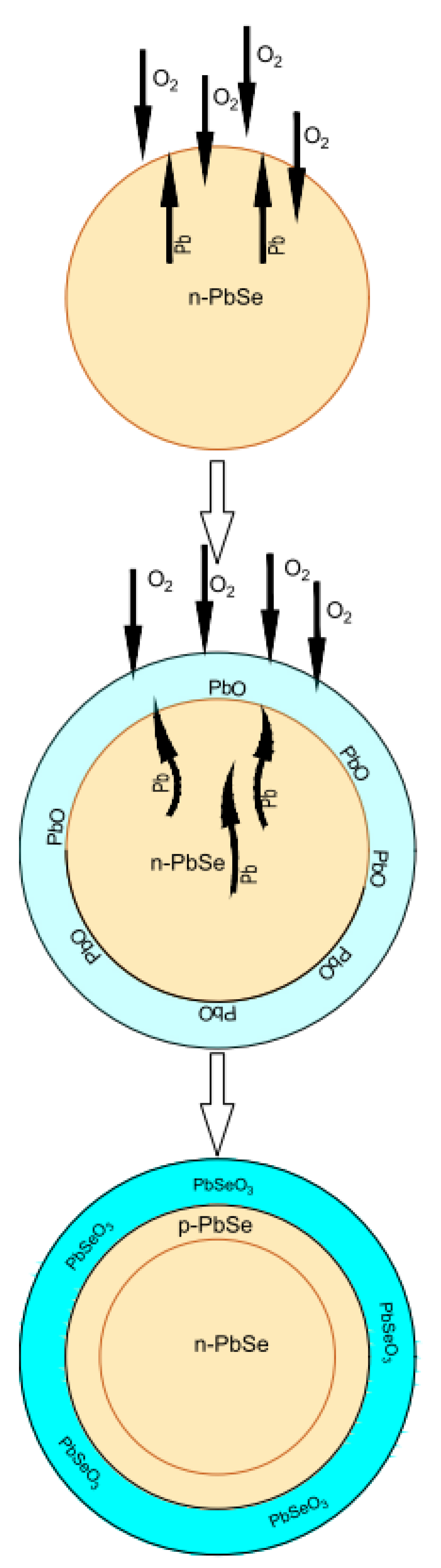
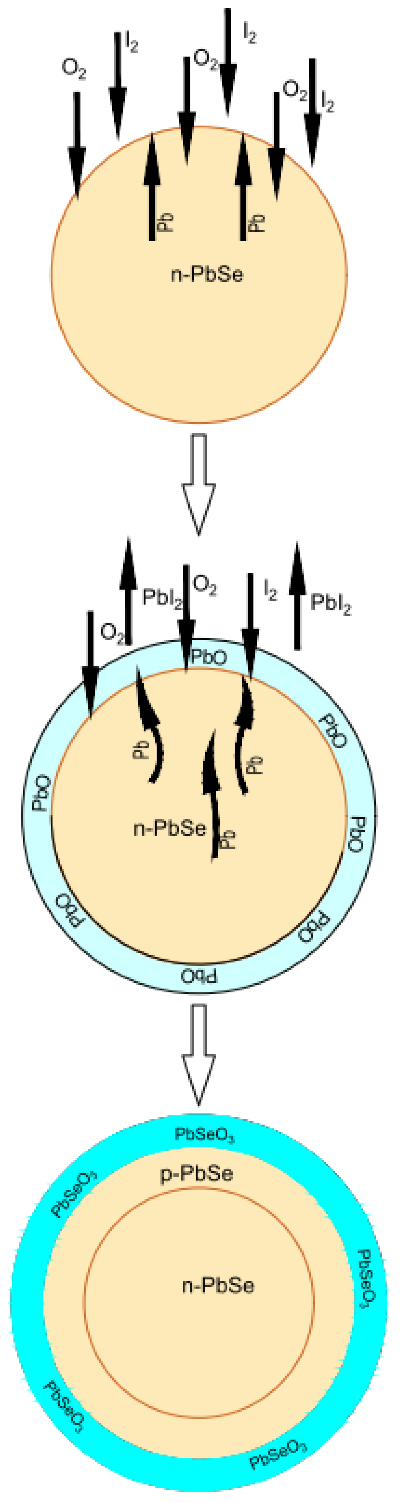
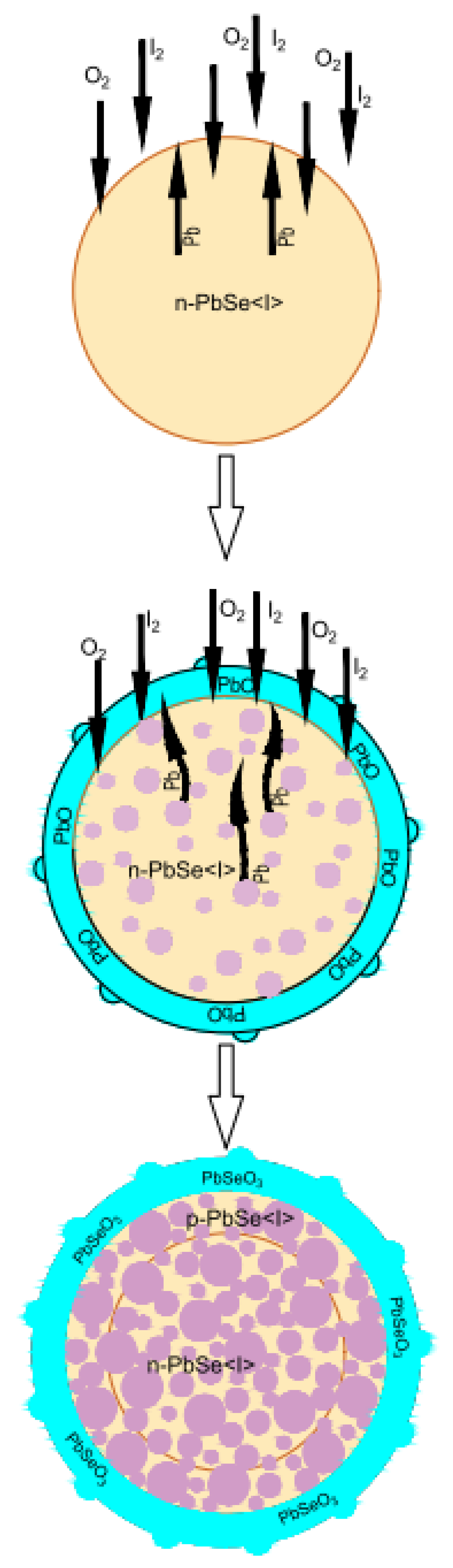
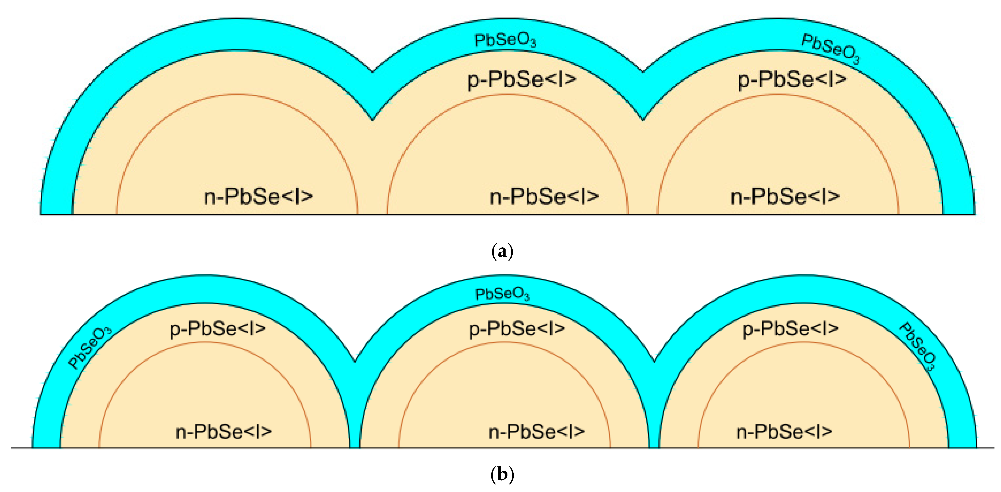
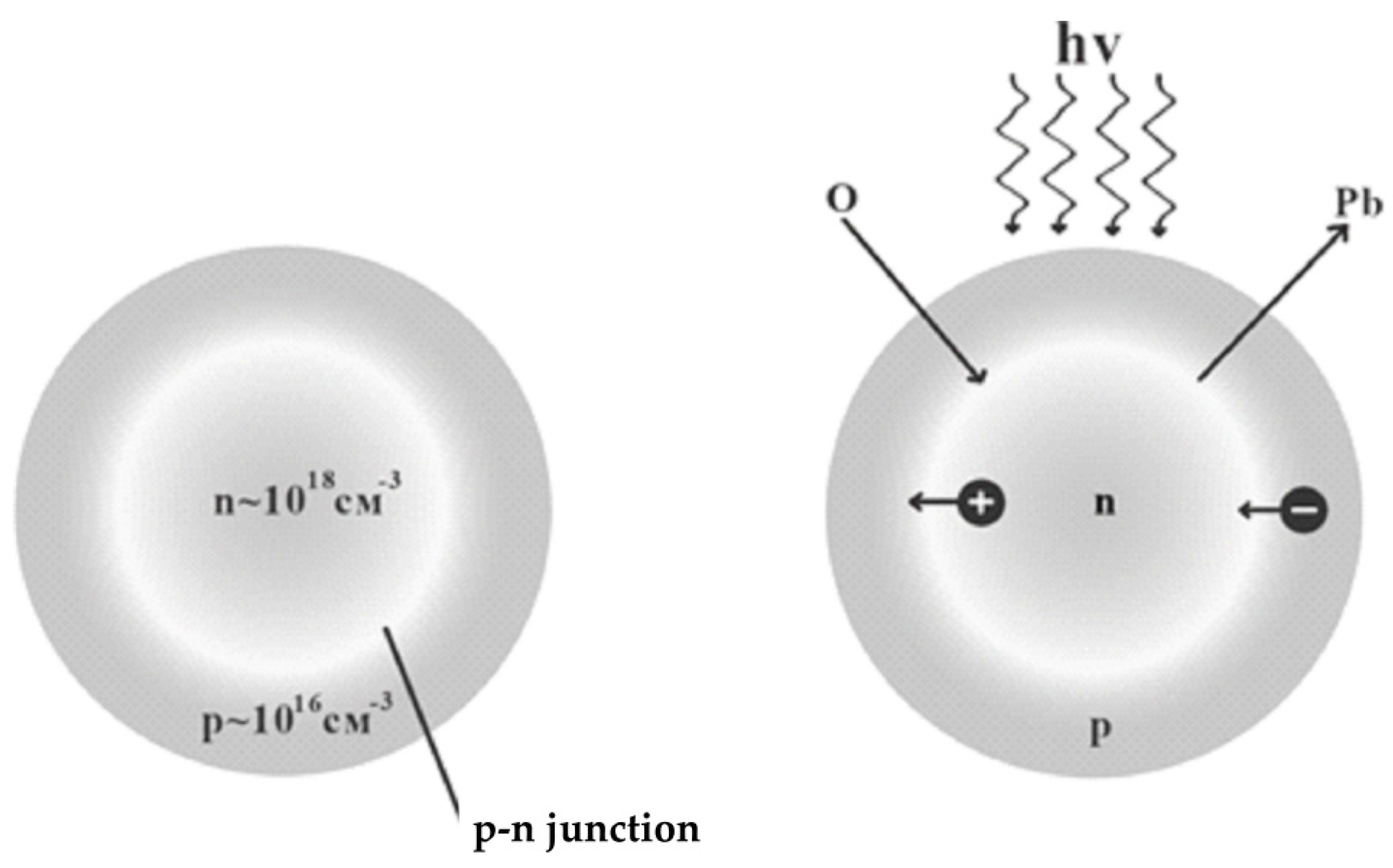
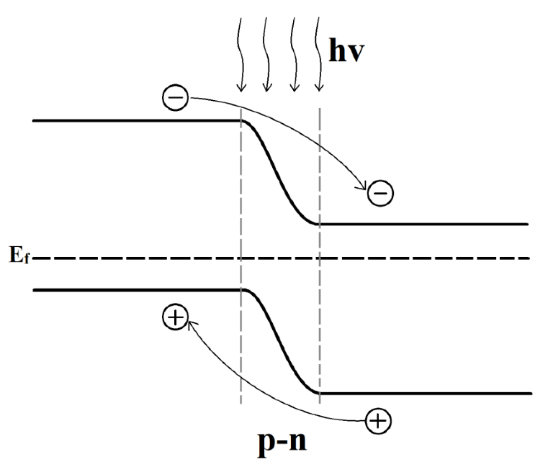
Development of the Model of the Porous Intragranular Architectonics

During the oxidation of the lead selenide grains in an oxygen-containing atmosphere, an outer shell of oxide phases is formed.
In this case, from the simplified triangulation model (a diagram of coexisting phases of the Pb-Se-O system was reviewed in [3]), one can see that for n-type PbSe, the formation of PbO due to Pb excess is typical, and so the lead chalcogenides grains changed to n-type conductivity.
So, the initial composition of the oxide is PbO. With a decrease in the concentration of charge carriers in the near-contact region with the oxide, the composition of the oxide tends to be oxyselenites and PbSeO3.
Subsequently, due to the growth of the shell, the Pb flow from the grain to the outside decreases, and the rate of its growth slows down until it stops completely.
Vacancies are formed due to the Kirkendall and Frenkel effects, because of the predominant departure of materials from the intragranular region. Thus, according to the diagram on the Gibbs triangle [3], the composition of the oxide approaches PbSeO3 or oxyselenites 4PbO·PbSeO3, 2PbO·PbSeO3. It was shown that oxide phases differing in composition and properties are formed depending on the annealing temperature [3]. Thus, at annealing temperatures in the range of 395–873 K, lead selenite PbSeO3 is formed predominantly, and at T ≥ 873 K, oxyselenites 2PbO ∙ PbSeO3, 4PbO ∙ PbSeO3 are formed.
In order to obtain highly efficient emitters, it is important that oxygen should penetrate deeply into the grain (Figure 4). This is due to the fact that oxygen acts like an acceptor dopant, forming a p–n junction and thereby improving the efficiency of the emitter. However, the formed oxide layers, increasing in thickness, impede the diffusion of oxygen. To reduce the rate of oxide growth and ensure the diffusion of oxygen into the grain, iodine is used (Figure 5).
In the presence of iodine vapor, the growth of the oxide layer slows down, because a metal atom coming out to the surface will react more efficiently with iodine than with oxygen, forming volatile lead and cadmium iodides.
Adding PbI2 and CdI2 compounds to the initial charge (Figure 6) provides the ability to control the organization (architectonics [9,20]) of the porosity of the intragranular space. Additionally, low-melting lead and cadmium iodides improve the crystalline quality of the material, reduce the probability of nonradiative recombination, and increase the photoluminescence efficiency.
Thus, the layer under the oxide coating possesses p-type conductivity. Deeper towards the center of the grain, the conductivity type changes, and the central (core) region itself has n-type conductivity. This structure has an internal p–n junction. Accordingly, it is expected that it will have photosensitive properties in the atomic–molecular design of the structure of the intragranular space, with a break in the percolation current flow in the n-regions. In practice, this is created by the through formation of p-layers at grain boundaries (Figure 7a).
Figure 7 shows a diagram of a constricting percolation cluster for a p-layer with a rupture of the flow along n-regions in the architectonics [14,19,20] of the photodetector (Figure 7a) and the architectonics [9,10,11] of the emitter—the paths of the flow are broken as in n-layers and along the p-layers (Figure 7b). For simplicity, the diagram shows the hierarchical level of communication between grains. The detailing of the hierarchical level corresponding to the structure of the intragranular space is not shown. The formation of porosity is important to increase the efficiency of emitters.
Under exposure of radiation in the layer sensitivity range (optical range 2–5 μm), an electron–hole pair is generated near the p–n junction. In the case of a photodetector, a change in the concentration of charge carriers in an initially lightly doped p-layer leads to a significant change in the conductivity and significant photosensitivity (Figure 8 and Figure 9).
In the case of emitting structures, the breakdown of both n- and p-type percolation channels is more effective (Figure 7b). In other words, the oxide layers must create insulating shells. Thus, the recombination of excited electron–hole pairs in intragranular regions will be more effective for photoluminescence.

4. Conclusions

A model is developed for the formation of porous, intragranular architectonics for photodetectors and IR emitters, based on nanostructured polycrystalline layers of lead chalcogenides obtained under conditions of thermal evaporation in a quasi-closed volume by the “hot wall” method, followed by sensitizing heat treatment in an iodine-containing atmosphere. The main regularities of the local molecular design and architectonics of infrared emitters of a new generation are characterized by the fact that in order to increase the photoluminescence efficiency, shell nanoelements with a developed intragranular structure are formed. The intragrain structure contains a developed system of pores and emitting centers with formed p–n junctions.

Author Contributions

Y.M.S.—paper writing, translation of the article into English, technology, methodology, AFM measurements, I.E.K.—development of model concepts, review of publications on the topic of the article, writing—review and editing, P.V.K.—modeling, creation of software products, model construction, paper writing and editing, Illustrations for the article and editing, V.A.M.—conceptualization, data curation, project administration, interpretation of the obtained results, editing, S.A.I.—modeling, creation of software products, model construction, editing. All authors have read and agreed to the published version of the manuscript.

Funding

This research received no external funding.

Conflicts of Interest

The authors declare no conflict of interest.

References

  1. Smerdov, R.; Mustafaev, A.; Spivak, Y.; Moshnikov, V. Functionalized nanostructured materials for novel plasma energy systems. In Topical Issues of Rational Use of Natural Resources 2019; CRC Press: London, UK, 2019; pp. 434–441. [Google Scholar] [CrossRef]
  2. Tomaev, V.; Levine, K.; Stoyanova, T.; Syrkov, A.G. Synthesis and Study of a Polypyrrole—Aluminum Oxide Nanocomposite Film on an Aluminum Surface. Glas. Phys. Chem. 2019, 45, 291–297. [Google Scholar] [CrossRef]
  3. Spivak, Y.U.; Moshnikov, V.A. Features of photosensitive polycrystalline PbCdSe layers with a network-like structure. J. Surf. Investig. X-ray Synchrotron Neutron Tech. 2010, 4, 71–76. [Google Scholar] [CrossRef]
  4. Salikhov, K.M.; Stoyanov, N.D.; Stoyanova, T.V. Using Optical Activation to Create Hydrogen and Hydrogen-Containing Gas Sensors. Key Eng. Mater. 2020, 854, 87–93. [Google Scholar] [CrossRef]
  5. Tomaev, V.V.; Levine, K.L.; Stoyanova, T.V.; Sirkov, A.G. Formation of nanocomposite film (polypirrol)/(aluminum) oxide on aluminum surface. AIP Conf. Proc. 2019, 2064, 030016. [Google Scholar]
  6. Gasanly, S.A.; Tomaev, V.V.; Stoyanova, T.V. The concept of the phases ratio control during the formation of composite filamentary nanocrystals xInSe-(1 − x)In2O3 on glass substrates. J. Phys. Conf. Ser. 2017, 917, 32021. [Google Scholar] [CrossRef]
  7. Syrkov, A.G. On the priority of Saint-Petersburg Mining University in the field of nanotechnology science and nanomaterials. Zap. Gorn. Inst. 2016, 221, 730–736. [Google Scholar]
  8. Pleskunov, I.V.; Syrkov, A.G. Razvitie issledovanij nizkorazmernyh metallosoderzhashchih sistem ot P.P.Vejmarna do nashih dnej. Zap. Gorn. Inst. 2018, 231, 287. (In Russian) [Google Scholar] [CrossRef]
  9. Katsuhiko, A. Progress in Molecular Nanoarchitectonics and Materials Nanoarchitectonics. Molecules 2021, 26, 1621. [Google Scholar]
  10. Ghosh, D.; Datta, L.P.; Govindaraju, T. Molecular architectonics of DNA for functional nanoarchitectures. Beilstein J. Nanotechnol. 2020, 11, 124–140. [Google Scholar] [CrossRef] [PubMed] [Green Version]
  11. Roy, B.; Ghosh, D.; Govindaraju, T. Molecular-architectonics-guided dynamic assembly to generate fluorescent organic nanoclusters with implications for optical imaging. ACS Appl. Nano Mater. 2021, 4, 979–984. [Google Scholar] [CrossRef]
  12. Afanas’ev, A.V.; Afanas’ev, V.P.; Glinskij, G.f.; Goloudina, S.I.; Gudovskih, A.S.; Demin, Y.U.A.; Dron’, A.S.; Zimina, T.M.; Zubkov, V.I.; Ivanov, S.A.; et al. Nanotekhnologiya: Fizika, Processy, Diagnostika, Pribory: Monografiya; Luchinina, V.V., Tairova, Y.M., Eds.; Fizmatlit: Moskva Russia, 2006; 552p. (In Russian) [Google Scholar]
  13. Karasev, V.A.; Luchinin, V.V. Vvedenie v Konstruirovanie Bionicheskih Nanosistem; Fizmatlit: Moscow, Russia, 2011. (In Russian) [Google Scholar]
  14. Wu, L.; Li, Y.; Fu, Z.; Su, B.-L. Hierarchically structured porous materials: Synthesis strategies and applications in energy storage. Natl. Sci. Rev. 2020, 7, 1667–1701. [Google Scholar] [CrossRef]
  15. Hammi, N.; El Hankari, S.; Katir, N.; Marcotte, N.; Draoui, K.; Royer, S.; El Kadib, A. Polysaccharide templated biomimetic growth of hierarchically porous metal-organic frameworks. Microporous Mesoporous Mater. 2020, 306, 110429. [Google Scholar] [CrossRef]
  16. Benjamin, R.T.; Horozov, T.S.; Paunov, V. Hierarchically structured composites and porous materials from soft templates: Fabrication and applications. J. Mater. Chem. A 2019, 7, 8030–8049. [Google Scholar]
  17. Lu, X.; Hasegawa, G.; Kanamori, K.; Nakanishi, K. Hierarchically porous monoliths prepared via sol–gel process accompanied by spinodal decomposition. J. Sol-Gel Sci. Technol. 2020, 95, 530–550. [Google Scholar] [CrossRef]
  18. Golubchenko, N.V.; Moshnikov, V.A.; Chesnokova, D.B. Investigation into the microstructure and phase composition of polycrystalline lead selenide films in the course of thermal oxidation. Glas. Phys. Chem. 2006, 32, 337–345. [Google Scholar] [CrossRef]
  19. Yang, X.-Y.; Chen, L.-H.; Li, Y.; Rooke, J.C.; Sanchez, C.; Su, B.-L. Hierarchically porous materials: Synthesis strategies and structure design. Chem. Soc. Rev. 2016, 46, 481–558. [Google Scholar] [CrossRef] [PubMed] [Green Version]
  20. Martin-Martinez, F.J.; Jin, K.; Barreiro, D.L.; Buehler, M.J. The Rise of Hierarchical Nanostructured Materials from Renewable Sources: Learning from Nature. ACS Nano 2018, 12, 7425–7433. [Google Scholar] [CrossRef]
  21. Shilova, O.A. Fractals, morphogenesis and triply periodic minimal surfaces in sol–gel-derived thin films. J. Sol-Gel Sci. Technol. 2020, 95, 599–608. [Google Scholar] [CrossRef]
  22. Khokhlov, D. Lead Chalcogenides: Physics and Applications; CRC Press: Boca Raton, FL, USA, 2002; 720p. [Google Scholar]
  23. Bordovskii, G.A.; Marchenko, A.; Anisimova, N.I.; Kozhokar, M.; Seregin, P.P. The state of tin impurity atoms in vitreous germanium chalcogenides. Glas. Phys. Chem. 2013, 39, 45–51. [Google Scholar] [CrossRef]
  24. Bordovskii, G.A.; Marchenko, A.V.; Kozhokar, M.; Nasredinov, F.S.; Seregin, P.P. Composition determination of multicomponent chalcogenide glassy semiconductors with X-ray fluorescence analysis. Glas. Phys. Chem. 2013, 39, 377–381. [Google Scholar] [CrossRef]
  25. Vasilev, E.; Kriulina, G.; Klepikov, I. Luminescence of natural diamond in the NIR range. Phys. Chem. Miner. 2020, 47, 1–8. [Google Scholar] [CrossRef]
  26. Vasilev, E.A. Luminescence of Plastically Deformed Diamond in the Range 800–1050 nm. J. Appl. Spectrosc. 2019, 86, 512–515. [Google Scholar] [CrossRef]
  27. Rykov, S.A. Scanning Probe Microscopy of Semiconductor Materials and Nanostructures; Shik, A.Y., Ed.; SPb.: Nauka, Russia, 2001; 52p. (In Russian) [Google Scholar]
  28. Maskaeva, L.N.; Yurk, V.; Markov, V.F.; Kuznetsov, M.V.; Voronin, V.I.; Muhamediarov, R.D.; Zyrianov, G.V. Composition, structure and functional properties of nanostructured PbSe films deposited using different antioxidants. Mater. Sci. Semicond. Process. 2019, 108, 104867. [Google Scholar] [CrossRef]
  29. Zlomanov, V.P. Obtaining and Research of Some Physicochemical Properties of Lead Selenide. Ph.D. Thesis, Chemistry Department of Moscow State University, Moscow, Russia, 1962. (In Russian). [Google Scholar]
  30. Tomaev, V.V.; Petrov, Y. Preparation of oxidized PbSeO3 films from PbSe films. Glas. Phys. Chem. 2012, 38, 240–244. [Google Scholar] [CrossRef]
  31. Alexandrova, O.A.; Maksimov, A.I.; Moshnikov, V.A.; Chesnokova, D.B. Chalcogenides and Oxides of IV Group Elements. Obtaining, Research, Application; Tekhnolit: St. Petersburg, Russia, 2008. (In Russian) [Google Scholar]
  32. Maraeva, E.V.; Moshnikov, V.A.; Tairov, Y.M. Models of the formation of oxide phases in nanostructured materials based on lead chalcogenides subjected to treatment in oxygen and iodine vapors. Semiconductors 2013, 47, 1422–1425. [Google Scholar] [CrossRef]
  33. Maraeva, E.V.; Moshnikov, V.A.; Petrov, A.A.; Tairov, Y.M. Oxidation model of polycrystalline lead-chalcogenide layers in an iodine-containing medium. Semiconductors 2016, 50, 775–777. [Google Scholar] [CrossRef]
  34. Maraeva, E.V. Obtaining and Studying Nanostructured Polycrystalline Layers and Quantum Dot Systems Based on Lead Chalcogenides. Ph.D. Thsis, St. Petersburg State Electrotechnical University “LETI” V.I. Ulyanov (Lenin), Saint Petersburg, Russia, 2014. (In Russian). [Google Scholar]
  35. Moshnikov, V.A.; Gamarts, A.E.; Chesnokova, D.B.; Maraeva, E.V. Growth and properties of nanostructured layers based on Pb1 − xCdxSe (x = 0–0.20) solid solutions. Inorg. Mater. 2011, 47, 18–22. [Google Scholar] [CrossRef]
  36. Zogg, H.; Ishida, A. IV-VI (Lead Chalcogenide) Infrared Sensors and Lasers. In Infrared Detectors and Emitters: Materials and Devices; Capper, P., Elliott, C.T., Eds.; Kluwer Academic Publishers: Boston, MA, USA, 2000; 478p. [Google Scholar]
  37. Lacome, T.; Montagne, X.; Delfort, B.; Paille, F. Diesel Fuel Compositions Containing Oxygenated Compounds Derived from Tetrahydrofurfuryl. U.S. Patent 20020053161A1, 9 May 2002. [Google Scholar]
  38. Maskaeva, L.N.; Vaganova, I.V.; Markov, V.F.; Voronin, V.I.; Mostovshchikova, E.V.; Belov, V.S.; Lipina, O.A.; Miroshnikova, I.N. A nonlinear evolution of the structure, morphology, and optical properties of PbS-CdS films with cadmium nitrate in the reaction mixture. Phys. Chem. Chem. Phys. 2021, 23, 10600–10614. [Google Scholar] [CrossRef] [PubMed]
  39. Chesnokova, D.B.; Moshnikov, V.A.; Gamarts, A.E.; Maraeva, E.V.; Aleksandrova, O.A.; Kuznetsov, V.V. Structural characteristics and photoluminescence of Pb1 − xCdxSe (x = 0–0.20) layers. J. Non-Cryst. Solids 2010, 356, 2010–2014. [Google Scholar] [CrossRef]
  40. Lopez-Otero, A. Hot wall epitaxy. Thin Solid Film. 1978, 49, 3–57. [Google Scholar] [CrossRef]
Figure 1. Scheme of reactor layout (left) and temperature distribution in it (right): 1—substrate heater; 2—holder of substrates; 3—substrate; 4—heater of the main steam source; 5—metal screens for leveling the temperature gradient; 6—damper divider; 7—capillary; 8—main load; 9—main charge thermocouple; 10—additional source of steam; 11—additional source of thermocouple; 12—heater of an additional source (Usub—substrate heater voltage, Ubasic and Uadd—main and additional heaters voltage of the reactor chamber walls, L—the length of the reactor zone, T—temperature).
Crystals 11 01143 g001
Figure 2. Experimental data of AFM of the photosensitive polycrystalline layer Pb1−xCdxSe <I> (x = 0.18) after plowing (force) lithography by AFM: (a) topography map (overall view of the surface), (b) the height profile along the line shown (a), (c) lateral force microscopy image recorded simultaneously with surface topography at (a) for the same sample area (d) image of a cross-section of an individual grain (arrows show the cross-section of oxidized layer covering the grains).
Crystals 11 01143 g002
Figure 3. Topography (a) and conductivity map (b) of the oxidized PbCdSe layer (under applied voltage is applied U = 5 V). (a), topography (c) and conductivity map (d) of the PbCdSe layer after removal of the oxidizing coating (when an external voltage is applied U = 2.5 V).
Crystals 11 01143 g003
Figure 4. The oxidation process of the n-PbSe grain (schematically).
Crystals 11 01143 g004
Figure 5. The oxidation process of the n-PbSe grain in the presence of I2 vapor (schematically).
Crystals 11 01143 g005
Figure 6. The oxidation process of n-PbSe grain with the presence of iodine in charge and in atmosphere during the annealing (forming voids are schematically shown as a purple spheres).
Crystals 11 01143 g006
Figure 7. Diagram of a constricting percolation cluster for a p-layer with a rupture of the flow along n-regions in the architectonics of the photodetector (a) and the architectonics of the emitter—the paths of the flow are broken as in n-layers and along the p-layers (b).
Crystals 11 01143 g007
Figure 8. The operation process of photosensitive structure (schematically).
Crystals 11 01143 g008
Figure 9. Energy diagram of the p–n junction region in photosensitive structure under illumination.
Crystals 11 01143 g009
Publisher’s Note: MDPI stays neutral with regard to jurisdictional claims in published maps and institutional affiliations.

