
Wide Bandwidth Silicon Nitride Strip-Loaded Grating Coupler on Lithium Niobate Thin Film


1
School of Sciences, Xi’an Technological University, Xi’an 710021, China
2
Zibo Vocational Institute, School of Intelligent Manufacturing, Zibo 255314, China
3
School of Physics, Shandong University, Jinan 250100, China
4
College of New Materials and New Energies, Shenzhen Technology University, Shenzhen 518118, China
*
Author to whom correspondence should be addressed.
Crystals 2022, 12(1), 70; https://0-doi-org.brum.beds.ac.uk/10.3390/cryst12010070
Submission received: 18 November 2021
/
Revised: 20 December 2021
/
Accepted: 31 December 2021
/
Published: 5 January 2022
(This article belongs to the Special Issue Nanocrystalline Materials: Preparation, Structural, Magnetic, Dielectric, Electrical, Optical, Thermal Properties and Applications (Volume II))
Abstract
:In this research, a vertical silicon nitride strip-loaded grating coupler on lithium niobate thin film was proposed, designed, and simulated. In order to improve the coupling efficiency and bandwidth, the parameters such as the SiO2 cladding layer thickness, grating period, duty cycle, fiber position, and fiber angle were optimized and analyzed. The alignment tolerances of the grating coupler parameters were also calculated. The maximum coupling efficiency and the −3 dB bandwidth were optimized to 33.5% and 113 nm, respectively. In addition, the grating coupler exhibited a high alignment tolerance.
1. Introduction
The emergence of lithium niobate on an insulator (LNOI) has greatly promoted the development and progress of integrated optics devices [1,2]. The high refractive index contrast between LN and SiO2 in LNOI can shrink the photonic devices/circuits and enhance the remarkable optical properties of LN [3,4,5,6]. Due to its extraordinary nonlinearity and excellent electrooptical properties, LNOI can be used in a variety of expandable on-chip devices to provide nonlinear wavelength conversion and high-speed optical modulation [7,8,9]. At present, it is very important to improve the coupling efficiency between an LNOI waveguide and fiber. However, the mode mismatch between optical fiber mode and thin film material makes direct alignment coupling inefficient. A grating coupler is an effective way to solve the coupling problem between an LNOI waveguide and optical fiber [10,11,12]. A grating coupler has many advantages, such as being able to be positioned anywhere on the chip, a large alignment tolerance, and no requirement for end face polishing.
Silicon nitride (Si3N4) has a wide transparent spectrum and high compatibility with the standard complementary metal oxide semiconductor technology [13,14]. It is difficult to etch directly on LN. However, this situation can be avoided by using Si3N4 strip loading. Si3N4 strip-loaded LNOI can make use of the properties of Si3N4 and LN, leading to heterogeneous photonic devices. Various photonic devices have been reported in Si3N4 strip-loaded LNOI, including a multiplexer [15], a micro-ring resonator [16], and an electrooptic modulator [17]. A large bandwidth can be obtained by using Si3N4 grating couplers, such as Si3N4-on-SOI grating couplers [18,19]. Modeling and simulation are indispensable steps in preparing high-quality grating.
In this study, an Si3N4 strip-loaded grating coupler on LNOI was studied and simulated based on the three-dimensional finite-difference time-domain method (3D-FDTD). The important parameters affecting the coupling efficiency of the grating coupler, including the grating period (Λ), duty cycle (DC = ω/Λ, where ω is the ridge width), the thickness of the SiO2 cladding layer (T), the fiber position x (distance between the grating edge and the fiber core in the x-axis, Lx), the fiber position y (distance between the center line of the grating and the fiber core in the y-axis, Ly), and the fiber angle (θ), were optimized, which provided guidance for improving the coupling efficiency of the grating couplers. The tolerance of the grating coupler was also carefully studied due to its great importance for the practical implementation of such a device.
2. Device Design and Methods
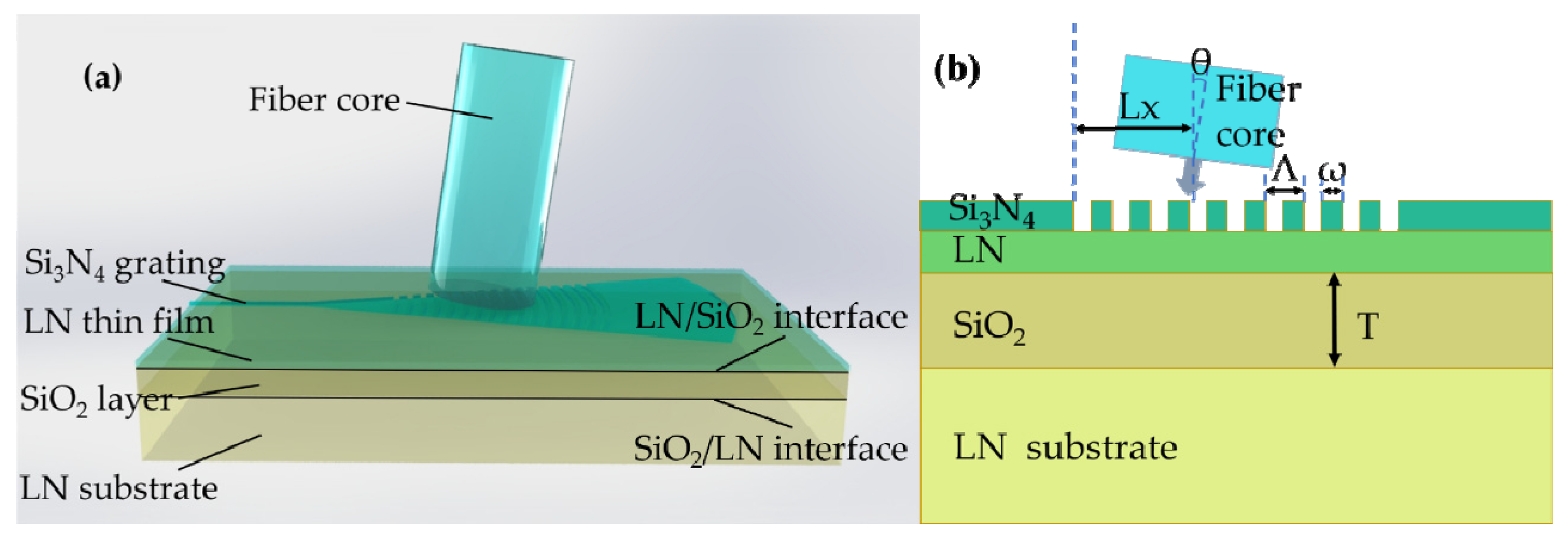
The structure of the Si3N4 strip-loaded grating coupler on LNOI that was studied from the top to bottom layers included a 0.3-μm-thick Si3N4 strip, a 0.5-μm-thick x-cut single-crystal LN thin film, an amorphous SiO2 cladding layer, and an LN substrate. The cross-sectional diagrams of the grating coupler are shown in Figure 1. The fiber fundamental transverse electric mode (TE0) was used as the light source to simulate the coupling process between the grating coupler and the optical fiber. Considering the single-mode operation, the small mode effective area, the optical power in the LN thin film, and the bending loss, the thickness of the Si3N4 strip-loaded grating coupler was selected as 0.3 μm [20], and it was fully etched. The thickness of the LN film was set to 0.5 μm. The parameters Λ, DC, T, Lx, Ly, and θ were varied to maximize the light coupling in the waveguide from the single-mode fiber.
The mechanism of the grating coupler is as follows: the light of a single-mode fiber was coupled to the grating structure because of the diffraction effect of the grating coupler. When the input field mode was matched to the waveguide mode, the light could be effectively coupled from the single-mode fiber to the waveguide plane. The overlap integral between the input field mode and the waveguide mode could be increased with the optimization of the parameters of the grating coupler to reduce the mode mismatch between the waveguide optical device and the single-mode fiber [21]. The coupling efficiency was defined as the percentage of power converted from the source power to the waveguide plane.
After diffracting through the grating coupler, part of the beam from the fiber was reflected back to the fiber, and part was scattered to the LN cladding. At the LN/SiO2 interface, part of the power was transmitted to the SiO2 cladding layer, and part of the power was reflected upwards and transmitted to the grating through the LN cladding layer again. The power was transmitted into the SiO2 cladding layer. At the SiO2/LN interface, part of the power that was lost was transmitted into the LN substrate, and part of the power was reflected and propagated upward through the SiO2 cladding to the LN cladding layer. Based on the commercial software Lumerical FDTD Solutions (Version: 8. 9.1584, ANSYS Inc., South Pittsburg, PA, USA) [22], the 3D-FDTD method under the condition of mess accuracy of 10 ppw (the number of mesh points per wavelength) was used for simulation and optimization, and the perfectly matched layer (PML) boundary conditions were used to absorb the light emitted from the simulation area. For the FDTD solutions [23], based on the solution of the vector three-dimensional Maxwell equations, the FDTD method was used to grid the space step-by-step in time based on the time-domain signal to obtain the steady-state continuous wave, resulting in a wide band, and the unique material model could accurately describe the dispersion characteristics of the material in a wide band with embedded high speed. A high-performance computing engine could be used to obtain wide band multiwavelength results in one calculation, simulate any three-dimensional shape, and provide an accurate dispersion material model. For the PML [22], due to the limitations of the computer memory capacity and the calculation speed, the FDTD calculation could only be carried out in a limited area. In order to simulate the propagation process of an ultrasonic wave in a larger area, it was necessary to set the absorption boundary conditions at the boundary of the area to absorb the incident waves and avoid reflecting waves as much as possible. The most common absorption boundary condition was the PML absorption boundary, which could theoretically achieve complete absorption.
3. Results and Discussion
According to the Bragg phase matching condition, the resonant excitation of the coupled mode is carried out when Equation (1) is satisfied [24]:
In the expression, is the wave number, q is the diffraction order (q = −1), θ is the incident angle, is the real part of the propagation constant, and is the effective refractive index of the guided mode. The range of the grating period can be estimated by using the above equation.
The grating coupler is sensitive to the effective refractive index, which has to fulfill the inequality , where and are the refractive indices of SiO2 (1.444) and LN (2.138) [25], respectively. The fiber angle θ, selected as 8°, can effectively avoid the second-order reflection that greatly reduces the coupling efficiency of the vertical grating coupler [26]. By substituting the inequality into Equation (1), the estimated range of Λ for the optical fiber angle can be obtained as . The range of Λ is estimated to be 0.775 µm ≤ Λ ≤ 1.188 µm.
In order to improve the coupling efficiency, the parameters of the grating coupler are analyzed and optimized. The thickness and the etching depth of the Si3N4 strip-loaded grating coupler are set to 0.3 μm. Due to the polarization sensitivity of the grating coupler, the fundamental TE mode is used in the simulation. The parameters of the TE polarized grating coupler are simulated and optimized. The results are shown in Table 1. The optimized coupling efficiency at a wavelength of 1.55 μm is 33.5%.
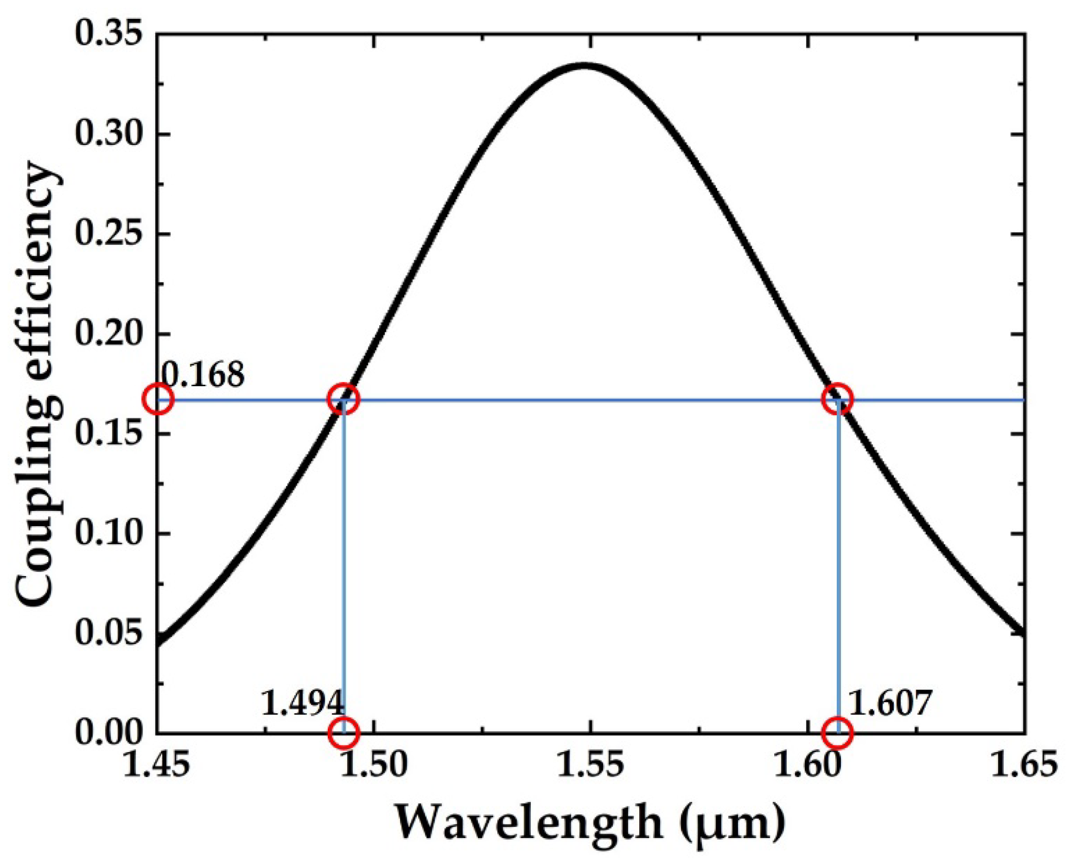
The relationship between the coupling efficiency and the wavelength is shown in Figure 2. The coupling efficiency is half of the peak value when the wavelengths of light are 1.494 and 1.607 μm. The −3 dB bandwidth is 113 nm. The simulation results show that the Si3N4 strip-loaded grating coupler on LNOI has a larger −3 dB bandwidth compared with the silicon strip-loaded grating coupler on LNOI [27].
In this simulation, the influence of each parameter on the performance of the grating coupler is studied using the control variable method. During the simulation, except for the modification of the studied parameter, the other parameters are fixed at their optimized values.
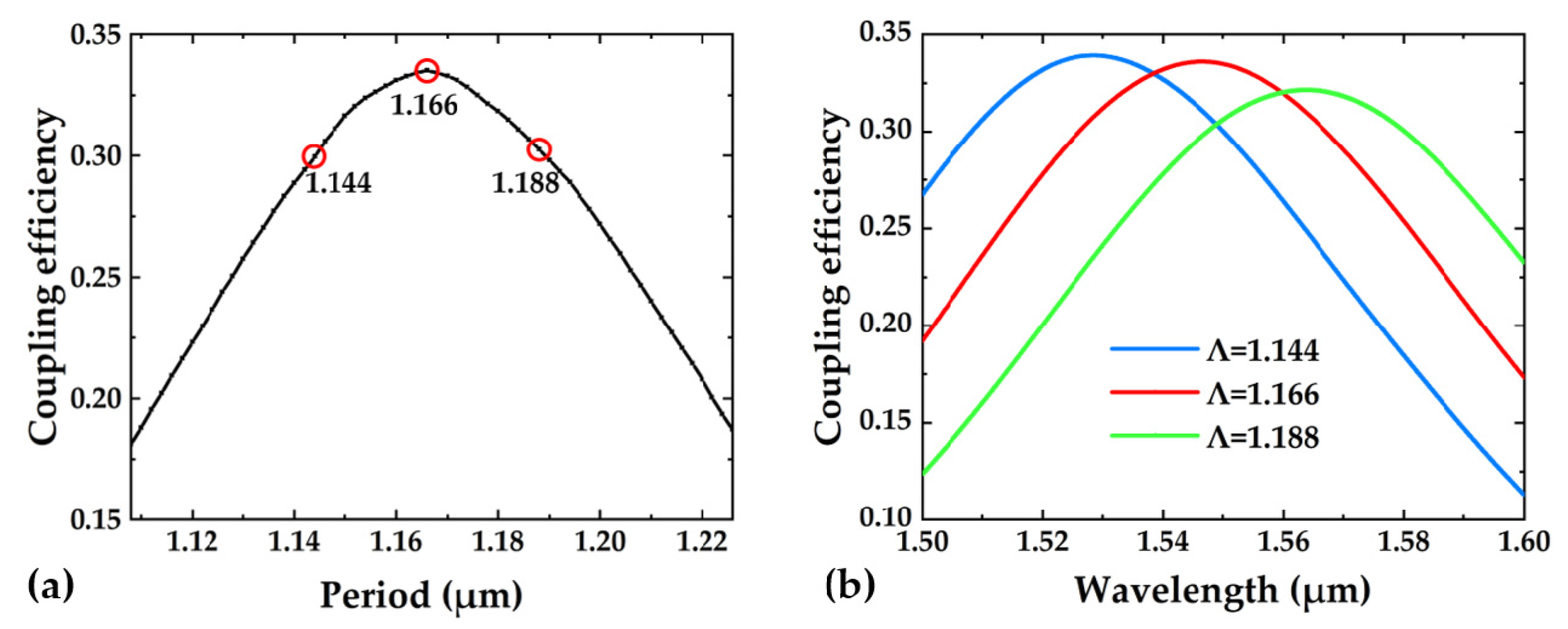
The relationship between the coupling efficiency and the grating period is shown in Figure 3a. When the grating period varies to 1.166 μm, the coupling efficiency reaches its maximum value. The coupling efficiency remains above 30% when the grating period deviates by 0.022 μm. The relationship between the coupling efficiency and the wavelength at different periods is shown in Figure 3b. The coupling efficiency at a wavelength of 1.55 μm corresponds to the red circles in Figure 3a. The peak of the coupling efficiency is red-shifted when the period increases, and it moves in the opposite direction when the period decreases.
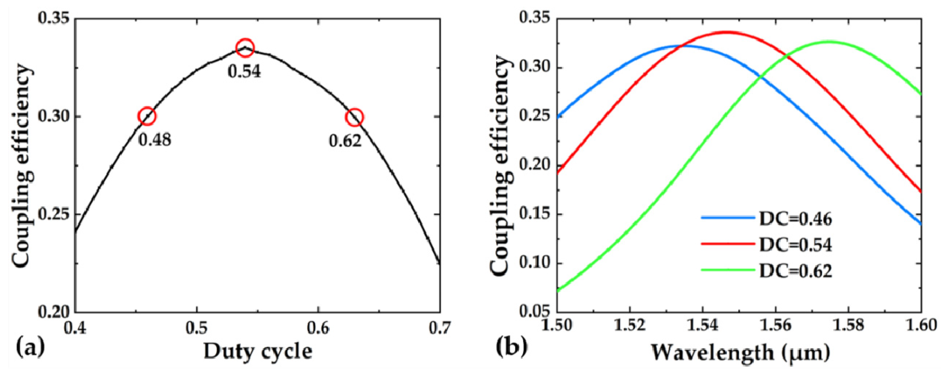
The relationship between the coupling efficiency and the duty cycle is shown in Figure 4a. The coupling efficiency reaches a peak when the duty cycle varies to 0.54. When the duty cycle deviates by 0.08, it retains a coupling efficiency of more than 30% at a wavelength of 1.55 μm. Figure 4b shows the variation of the coupling efficiency with wavelengths for different duty cycles. The coupling efficiency at a wavelength of 1.55 μm in Figure 4b corresponds to the red circles in Figure 4a. The peak of the coupling efficiency is red-shifted when the duty cycle increases, and it moves in the opposite direction when the duty cycle decreases.
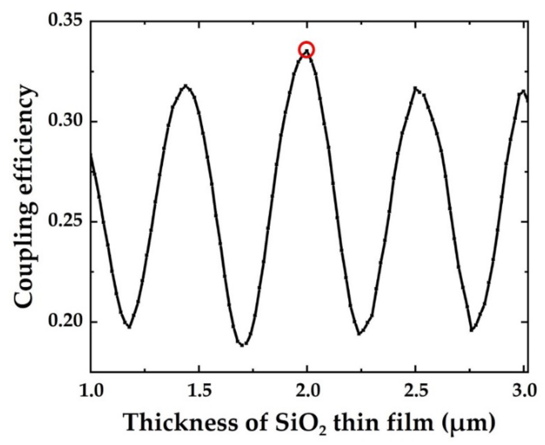
The relationship between the coupling efficiency and the SiO2 cladding layer thickness is shown in Figure 5. The curve of the coupling efficiency oscillates periodically between the maximum and the minimum as the thickness of the SiO2 cladding layer increases. The periodic variation of the coupling efficiency stems from the constructive or destructive interference between the upward reflected light from the LN/SiO2 interface and the SiO2/LN interface.
Figure 6a,b shows the coupling efficiencies as functions of Lx and Ly, respectively. Since the grating coupler is symmetrical in the y-direction, only half of Ly is simulated. The coupling efficiencies reach their peaks when Lx and Ly are set at 4.8 μm and 1 μm, respectively. The coupling efficiency decreases faster when Lx decreases than when Lx increases. The coupling efficiency decreases to 30% when Lx is 3 μm and 7.2 μm. When Ly is less than 5 μm, the coupling efficiency is almost unchanged. However, the coupling efficiency begins to decrease rapidly when Ly is 6 μm, while the coupling efficiency decreases sharply to 29%.
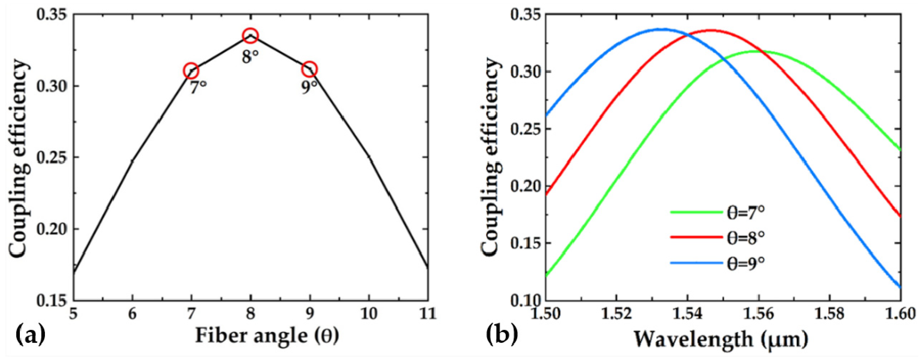
Figure 7a shows the relationship between the coupling efficiency and the fiber angle. The coupling efficiency is very sensitive to the change of the fiber angle. The coupling efficiency decreases very little when the fiber angle deviates by 1°. However, the coupling efficiency decreases rapidly when the fiber angle deviates by 2°. The peak of the coupling efficiency is red-shifted when the fiber angle decreases, and it moves in the opposite direction when the fiber angle increases.
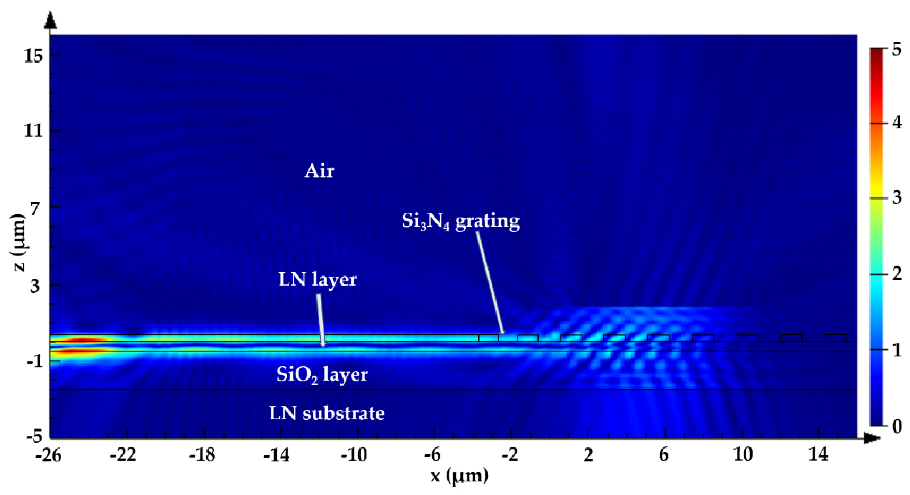
Figure 8 shows the electric field distribution of the light wave. The in-coupled light formed an angle (8°) relative to the normal of the LN substrate. This angle allows the grating coupler to achieve near-vertical coupling in the waveguide plane at wavelengths of around 1.55 μm while avoiding second-order reflection. The light from the optical fiber is mainly divided into three parts: some scatter upwards into the air due to reflection, some are coupled into the waveguide, and others are lost in the substrate.
Table 2 lists a comparison of the different types of grating couplers previously reported on and the coupler in this work. The chirped grating couplers and grating couplers using the bottom or top reflectors have higher coupling efficiencies than uniform grating couplers. In this work, the maximum coupling efficiency of the LNOI coupler using uniform Si3N4 strip loading is 33.5%, and the −3 dB bandwidth is 113 nm. It can be confirmed that the grating coupler is a reliable method for solving the coupling between the chip and the single-mode fiber, and a wide −3 dB bandwidth can be obtained by using Si3N4 strip loading.
4. Conclusions
In this work, a 3D-FDTD simulation technique was used to systematically study the performance of an Si3N4 strip-loaded grating coupler on LNOI. The light was coupled vertically into the LNOI waveguide from a single-mode fiber. The parameters Λ, DC, T, Lx, Ly, and θ were analyzed and optimized to be 1.166 μm, 0.54, 2 μm, 4.8 μm, 1 μm, and 8°, respectively. At wavelengths of around 1.55 μm, the maximums of the coupling efficiency and the −3 dB bandwidth were 33.5% and 113 nm, respectively. The relationship between the parameter tolerance and the coupling efficiency of the grating couplers was discussed. Larger tolerances greatly reduced the requirements for manufacturing accuracy. Our simulation results for the grating couplers will provide useful guidance for the fabrication of similar optical devices.
Author Contributions
H.H. conceived the original idea; F.Y. carried out the simulations and wrote the manuscript; and H.F. and B.X. contributed the useful and deep discussions, analyzed the data, and modified the manuscript. All authors have read and agreed to the published version of the manuscript.
Funding
This work was supported by the National Natural Science Foundation of China (12105190) and Shenzhen Science and Technology Planning (JCYJ20190813103207106).
Data Availability Statement
Data will be made available upon request.
Conflicts of Interest
The authors declare no conflict of interest.
References
- Poberaj, G.; Hu, H.; Sohler, W.; Gunter, P. Lithium niobate on insulator (LNOI) for micro-photonic devices. Laser Photonics Rev. 2012, 6, 488–503. [Google Scholar] [CrossRef]
- Boes, A.; Corcoran, B.; Chang, L.; Bowers, J.; Mitchell, A. Status and Potential of Lithium Niobate on Insulator (LNOI) for Photonic Integrated Circuits. Laser Photonics Rev. 2018, 12, 1700256. [Google Scholar] [CrossRef]
- Wang, C.; Zhang, M.; Chen, X.; Bertrand, M.; Shams-Ansari, A.; Chandrasekhar, S.; Winzer, P.; Lončar, M. Integrated lithium niobate electro-optic modulators operating at CMOS-compatible voltages. Nature 2018, 562, 101–104. [Google Scholar] [CrossRef]
- Han, H.; Cai, L.; Hu, H. Optical and structural properties of single-crystal lithium niobate thin film. Opt. Mater. 2015, 42, 47–51. [Google Scholar] [CrossRef]
- Xu, M.; He, M.; Zhang, H.; Jian, J.; Pan, Y.; Liu, X.; Chen, L.; Meng, X.; Chen, H.; Li, Z.; et al. High-performance coherent optical modulators based on thin-film lithium niobate platform. Nat. Commun. 2020, 11, 3911–3917. [Google Scholar] [CrossRef]
- Cai, L.; Han, H.; Zhang, S.; Hu, H.; Wang, K. Photonic crystal slab fabricated on the platform of lithium niobate-on-insulator. Opt. Lett. 2014, 39, 2094–2096. [Google Scholar] [CrossRef]
- Luo, K.-H.; Brauner, S.; Eigner, C.; Sharapova, P.R.; Ricken, R.; Meier, T.; Herrmann, H.; Silberhorn, C. Nonlinear integrated quantum electro-optic circuits. Sci. Adv. 2019, 5, eaat1451. [Google Scholar] [CrossRef] [Green Version]
- Li, M.; Ling, J.; He, Y.; Javid, U.A.; Xue, S.; Lin, Q. Lithium niobate photonic-crystal electro-optic modulator. Nat. Commun. 2020, 11, 4123–4130. [Google Scholar] [CrossRef]
- Wang, C.; Zhang, M.; Yu, M.; Zhu, R.; Hu, H.; Loncar, M. Monolithic lithium niobate photonic circuits for Kerr frequency comb generation and modulation. Nat. Commun. 2019, 10, 978–983. [Google Scholar] [CrossRef]
- Cai, L.; Piazza, G. Low-loss chirped grating for vertical light coupling in lithium niobate on insulator. J. Opt. 2019, 21, 065801. [Google Scholar] [CrossRef]
- Han, H.; Xiang, B. Grating Coupler Design for Vertical Light Coupling in Silicon Thin Films on Lithium Niobate. Crystals 2020, 10, 850. [Google Scholar] [CrossRef]
- Chen, Z.; Peng, R.; Wang, Y.; Zhu, H.; Hu, H. Grating coupler on lithium niobate thin film waveguide with a metal bottom reflector. Opt. Mater. Express 2017, 7, 4010–4017. [Google Scholar] [CrossRef]
- Romero-García, S.; Merget, F.; Zhong, F.; Finkelstein, H.; Witzens, J. Silicon nitride CMOS-compatible platform for integrated photonics applications at visible wavelengths. Opt. Express 2013, 21, 14036–14046. [Google Scholar] [CrossRef]
- Ahmed, A.N.R.; Mercante, A.; Shi, S.; Yao, P.; Prather, D.W. Vertical mode transition in hybrid lithium niobate and silicon nitride-based photonic integrated circuit structures. Opt. Lett. 2018, 43, 4140–4143. [Google Scholar] [CrossRef] [Green Version]
- Liu, Y.; Huang, X.; Li, Z.; Guan, H.; Yu, H.; Wei, Q.; Fan, Z.; Han, W.; Li, Z. On-chip four-mode (de-)multiplexer on thin film lithium niobite-silicon rich nitride hybrid platform. Opt. Lett. 2021, 46, 3179–3182. [Google Scholar] [CrossRef] [PubMed]
- Ahmed, A.N.R.; Shi, S.; Zablocki, M.; Yao, P.; Prather, D.W. Tunable hybrid silicon nitride and thin-film lithium niobate electro-optic microresonator. Opt. Lett. 2019, 44, 618–621. [Google Scholar] [CrossRef] [Green Version]
- Zhang, P.; Huang, H.; Jiang, Y.; Han, X.; Xiao, H.; Frigg, A.; Nguyen, T.G.; Boes, A.; Ren, G.; Su, Y.; et al. High-speed electro-optic modulator based on silicon nitride loaded lithium niobate on an insulator platform. Opt. Lett. 2021, 46, 5986–5989. [Google Scholar] [CrossRef]
- Sacher, W.D.; Huang, Y.; Ding, L.; Taylor, B.J.F.; Jayatilleka, H.; Lo, G.-Q.; Poon, J.K.S. Wide bandwidth and high coupling efficiency Si_3N_4-on-SOI dual-level grating coupler. Opt. Express 2014, 22, 10938–10947. [Google Scholar] [CrossRef]
- Doerr, C.R.; Chen, L.; Chen, Y.-K.; Buhl, L.L. Wide Bandwidth Silicon Nitride Grating Coupler. IEEE Photonics-Technol. Lett. 2010, 22, 1461–1463. [Google Scholar] [CrossRef]
- Han, H.; Yang, F.; Liu, C.; Jiang, Y.; Xiang, B.; Ruan, C. High-performance electro-optical Mach–Zehnder modulator in silicon nitride-lithium niobate thin film hybrid platform. Opt. Express 2022. in submit. [Google Scholar]
- Cheng, L.; Mao, S.; Li, Z.; Han, Y.; Fu, H.Y. Grating Couplers on Silicon Photonics: Design Principles, Emerging Trends and Practical Issues. Micromachines 2020, 11, 666. [Google Scholar] [CrossRef]
- Solutions, L. Available online: http://www.lumerical.com/ (accessed on 18 November 2021).
- Shibayama, J.; Ando, R.; Yamauchi, J.; Nakano, H. A 3-D LOD-FDTD Method for the Wideband Analysis of Optical Devices. J. Lightwave Technol. 2011, 29, 1652–1658. [Google Scholar] [CrossRef]
- Mu, X.; Wu, S.; Cheng, L.; Fu, H.Y. Edge Couplers in Silicon Photonic Integrated Circuits: A Review. Appl. Sci. 2020, 10, 1538. [Google Scholar] [CrossRef] [Green Version]
- Schlarb, U.; Betzler, K. A generalized sellmeier equation for the refractive indices of lithium niobate. Ferroelectrics 1994, 156, 99–104. [Google Scholar] [CrossRef]
- Vivien, L.; Pascal, D.; Lardenois, S.; Marris-Morini, D.; Cassan, E.; Grillot, F.; Laval, S.; Fédéli, J.-M.; Melhaoui, L.M. Light injection in SOI microwaveguides using high-efficiency grating couplers. J. Lightwave Technol. 2006, 24, 3810–3814. [Google Scholar] [CrossRef]
- Ma, X.; Zhuang, C.; Zeng, R.; Coleman, J.J.; Zhou, W. Polarization-independent one-dimensional grating coupler design on hybrid silicon/LNOI platform. Opt. Express 2020, 28, 17113–17121. [Google Scholar] [CrossRef] [PubMed]
- Chen, Z.; Ning, Y.; Xun, Y. Chirped and apodized grating couplers on lithium niobate thin film. Opt. Mater. Express 2020, 10, 2513–2521. [Google Scholar] [CrossRef]
- Baghban, M.A.; Schollhammer, J.; Errando-Herranz, C.; Gylfason, K.B.; Gallo, K. Bragg gratings in thin-film LiNbO_3 waveguides. Opt. Express 2017, 25, 32323–32332. [Google Scholar] [CrossRef]
- Jian, J.; Xu, P.; Chen, H.; He, M.; Wu, Z.; Zhou, L.; Liu, L.; Yang, C.; Yu, S. High-efficiency hybrid amorphous silicon grating couplers for sub-micron-sized lithium niobate waveguides. Opt. Express 2018, 26, 29651–29658. [Google Scholar] [CrossRef]
- Chen, B.; Ruan, Z.; Hu, J.; Wang, J.; Lu, C.; Lau, A.P.T.; Guo, C.; Chen, K.; Chen, P.; Liu, L. Two-dimensional grating coupler on an X-cut lithium niobate thin-film. Opt. Express 2021, 29, 1289–1295. [Google Scholar] [CrossRef]
- Zhang, Z.; Shan, X.; Huang, B.; Zhang, Z.; Cheng, C.; Bai, B.; Gao, T.; Xu, X.; Zhang, L.; Chen, H. Efficiency Enhanced Grating Coupler for Perfectly Vertical Fiber-to-Chip Coupling. Materials 2020, 13, 2681. [Google Scholar] [CrossRef] [PubMed]
Figure 1.
(a) The structure diagram, and (b) schematic cross-section of an Si3N4 strip-loaded grating coupler on LNOI.
Figure 1.
(a) The structure diagram, and (b) schematic cross-section of an Si3N4 strip-loaded grating coupler on LNOI.

Figure 2.
Coupling efficiency as a function of wavelength.

Figure 3.
(a) Coupling efficiency as a function of the period. (b) Coupling efficiency as a function of the wavelength at different periods.
Figure 3.
(a) Coupling efficiency as a function of the period. (b) Coupling efficiency as a function of the wavelength at different periods.

Figure 4.
(a) Coupling efficiency as a function of the duty cycle. (b) Coupling efficiency as a function of the wavelength at different duty cycles.
Figure 4.
(a) Coupling efficiency as a function of the duty cycle. (b) Coupling efficiency as a function of the wavelength at different duty cycles.

Figure 5.
Coupling efficiency as a function of the SiO2 cladding thickness.

Figure 6.
(a) Coupling efficiency as a function of Lx. (b) Coupling efficiency as a function of Ly.

Figure 7.
(a) Coupling efficiency as a function of the fiber angle. (b) Coupling efficiency as a function of the wavelength at different fiber angles.
Figure 7.
(a) Coupling efficiency as a function of the fiber angle. (b) Coupling efficiency as a function of the wavelength at different fiber angles.

Figure 8.
Electric field distribution of the light wave.


Table 1.
The optimized parameters of the Si3N4 strip-loaded grating coupler at a wavelength of 1.55 μm.
Table 1.
The optimized parameters of the Si3N4 strip-loaded grating coupler at a wavelength of 1.55 μm.
| Λ (µm) | DC | T (μm) | Lx (μm) | Ly (μm) | θ (°) |
|---|---|---|---|---|---|
| 1.166 | 0.54 | 2 | 4.8 | 1 | 8 |
Table 2.
A comparison of the reported grating couplers in this work.
| Grating Coupler Type | Features | Coupling Efficiency (%) | Bandwidth (nm) | Ref |
|---|---|---|---|---|
| LN-on-SiO2 | Chirped grating coupler | 43.7 (TE) (1550 nm) | 48 (−3 dB) | [10] |
| Si3N4-on-SOI | Apodized grating coupler | 79.4 (TE) (1550 nm) | 80 (−1 dB) | [16] |
| Si-on-LNOI | Polarization-independent | 50.1 (TE) (1550 nm) | 86 (−3 dB) | [17] |
| LN-on-SiO2 | Chirped and apodized grating coupler | 83.2 (TE) (1536 nm) | 82 (−3 dB) | [28] |
| LN-on-SiO2 | Integrated coupler and filter | 14.5 (TE) (1550 nm) | 80 (−3 dB) | [29] |
| Si-SiO2-LN | Fully etched grating | 53.7 (TE) (1550 nm) | 102 (−3 dB) | [30] |
| LN-on-SiO2 | Metal bottom reflector | 45.7 (TE) (1553.5 nm) | 30 (−1 dB) | [31] |
| Si-on-SiO2 | Uniform grating with upper reflector | 89.4 (TE) (~1550 nm) | 96 (−3 dB) | [32] |
| Si3N4-on-LNOI | Strip-loaded uniform grating | 33.5 (TE) (1550 nm) | 113 (−3 dB) | This work |
Publisher’s Note: MDPI stays neutral with regard to jurisdictional claims in published maps and institutional affiliations. |
© 2022 by the authors. Licensee MDPI, Basel, Switzerland. This article is an open access article distributed under the terms and conditions of the Creative Commons Attribution (CC BY) license (https://creativecommons.org/licenses/by/4.0/).
Share and Cite
MDPI and ACS Style
Yang, F.; Fang, H.; Han, H.; Xiang, B. Wide Bandwidth Silicon Nitride Strip-Loaded Grating Coupler on Lithium Niobate Thin Film. Crystals 2022, 12, 70. https://0-doi-org.brum.beds.ac.uk/10.3390/cryst12010070
AMA Style
Yang F, Fang H, Han H, Xiang B. Wide Bandwidth Silicon Nitride Strip-Loaded Grating Coupler on Lithium Niobate Thin Film. Crystals. 2022; 12(1):70. https://0-doi-org.brum.beds.ac.uk/10.3390/cryst12010070
Chicago/Turabian StyleYang, Fan, Hong Fang, Huangpu Han, and Bingxi Xiang. 2022. "Wide Bandwidth Silicon Nitride Strip-Loaded Grating Coupler on Lithium Niobate Thin Film" Crystals 12, no. 1: 70. https://0-doi-org.brum.beds.ac.uk/10.3390/cryst12010070
Note that from the first issue of 2016, this journal uses article numbers instead of page numbers. See further details here.