
A Theoretical Modeling of Adaptive Mixed CNT Bundles for High-Speed VLSI Interconnect Design


1
Department of Electrical and Computer Engineering, University of Massachusetts Amherst (UMass), 100 Natural Resources Road, Amherst, MA 01003, USA
2
Department of Electrical and Computer Engineering, Florida Polytechnic University, 4700 Research Way, Lakeland, FL 33805, USA
*
Author to whom correspondence should be addressed.
Crystals 2022, 12(2), 186; https://0-doi-org.brum.beds.ac.uk/10.3390/cryst12020186
Submission received: 14 November 2021
/
Revised: 24 January 2022
/
Accepted: 24 January 2022
/
Published: 27 January 2022
(This article belongs to the Special Issue Fabrication of Carbon and Related Materials/Metal Hybrids and Composites)
Abstract
:The aroused quest to reduce the delay at the interconnect level is the main urge of this paper, so as to come across a configuration of carbon nanotube (CNT) bundles, namely, squarely packed bundles of mixed CNTs. The demonstrated approach in this paper makes the mixed CNT bundle adaptable to adopt for high-speed very-large-scale integration (VLSI) interconnects with technology shrinkage. To reduce the delay of the proposed configuration of the mixed CNT bundle, the behavioral change of resistance (R), inductance (L), and capacitance (C) has been observed with respect to both the width of the bundle and the diameter of the CNTs in the bundle. Consequently, the performance of the modified bundle configuration is compared with a previously developed configuration, namely, squarely packed bundles of dimorphic MWCNTs in terms of propagation delay and crosstalk delay at local-, semiglobal-, and global-level interconnects. The proposed bundle configuration is, ultimately, enacted as the better one for 32-nm and 16-nm technology nodes, and is suitable for 7-nm nodes as well.
1. Introduction
The overwhelming exploitation of interconnects to the device delay makes researchers weigh Carbon Nanotubes (CNTs) for the possession pertinent to long mean free path [1], electrical properties [1,2], thermal properties [2,3], electromigration, and current density [4]. Moreover, crosstalk delay is a potential stymie for CNTs due to capacitive coupling between adjacent bundles [5]. While it is brought up, in previous literature [1], that the performance will be meliorated with further technology scaling, CNTs can render much better performance based on the exploration of some features.
It is claimed in [5,6] that mutual inductance does not have a considerable impact on crosstalk-induced delay and glitches; instead, coupling capacitance with electrostatic and quantum capacitance makes the main contribution. It is also noticed in [7] that the graphitized electron beam-induced deposition (EBID) carbon has the capability to produce a low-resistance ohmic contact to multiple shells of MWCNT, in the context of making high-performance electrical interconnect structures for next-generation electronic circuits. Although the densely packed configuration of bundled CNTs is seizing attention for improving performance, a trade-off between propagation delay and crosstalk delay is conspicuous [8]. Having noticed, from earlier work [5], that SWCNT and DWCNT shows poorer performance than Cu-based interconnects, owing to higher coupling capacitances, we endeavored to avoid putting any SWCNTs and DWCNTs on the edge of the bundle in our configuration.
To improve the crosstalk delay along with propagation delay, some works [6,9,10,11,12] are conducted by introducing different bundle configurations and by combining both MWCNT and SWCNT in the bundle. Rai et al. claimed that the structure with MWCNTs surrounded by SWCNTs yields better performance by considering the tunnelling and intershell coupling between adjacent shells by depicting four different structures in [10]. The same group, subsequently, showed that the structure with SWCNTs and MWCNTs possessing equal halves vertically was the best one in terms of frequency noise amplitude by delineating the same four structures in another work [11]. However, it is demonstrated in [6,9] that, by varying the relative position of MWCNTs and SWCNTs in the bundle, CNTs with spatial distribution, putting the SWCNTs entirely wrapped up by the MWCNTs in the bundle, indulges lower crosstalk delay than those with random arrangements. A delay-efficient configuration of a mixed bundle is proposed in [12] as well, though the crosstalk delay performance of this configuration is not well-proved since this work opposes the fact, mentioned in [6,9], that SWCNTs are mounted over the boundary of the bundle.
The aim of this paper is to present an innovative diameter-controlled configuration to alleviate the propagation delay and crosstalk delay of size shrinking interconnects, which is feasible from the fabrication aspect. This configuration is presented here with a detailed theoretical and mathematical model analysis and comparison results to assure better enquiries of its performance and enlighten its advantages. To analyze the delay performance, the analytical delay model has been obtained using the parameters from previous works [13,14,15,16].
The rest of this paper is organized in the following manner. A modified configuration of a mixed CNT bundle is proposed and illustrated in Section 2. Section 3 is used to develop the mathematical models for elements for isolated CNTs, and eventually for a mixed bundle based on the configuration introduced in Section 2. Section 4 is dedicated to the interest of simulating and analyzing the performance indicators, propagation delay, and crosstalk noise for different technology nodes, and depicting a graphical comparison with the previously well-developed research work [17,18]. Section 5 comes up with the conclusion by appending the future work potentialities and improvements.
2. Modified Mixed CNT Bundle Configuration
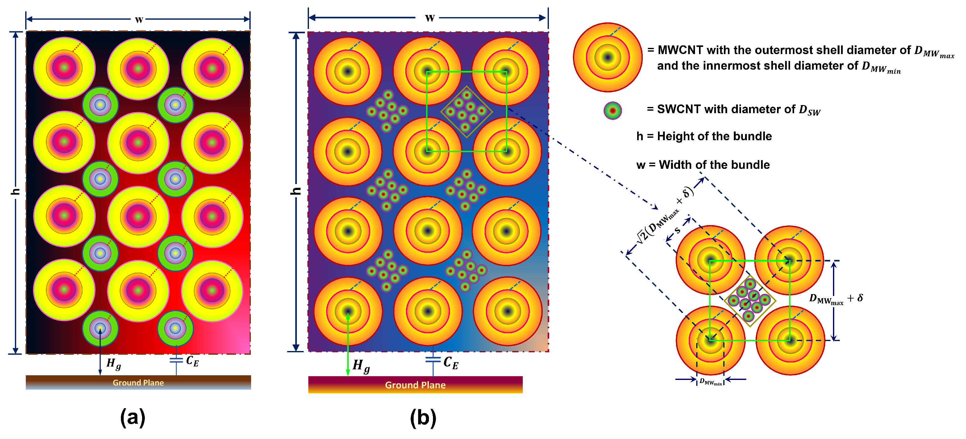
Our endeavor in this paper is to enhance the performance by altering the configuration, shown in Figure 1a. In this newly introduced configuration, illustrated in Figure 1b, the replacement of smaller MWCNTs takes place with a bunch of SWCNTs, which are wrapped up by the larger MWCNTs. This modified approach is a virtue of increasing the number of CNTs in the bundle so that we can fill up the unoccupied space with SWCNTs more efficiently and densely. The spacing between shells of MWCNTs and adjacent CNTs, equivalent to the van der Waals distance () between graphene layers in graphite, is maintained concurrently [19,20].
The proposed configuration is inspired by the geometric pattern previously proposed in the works [17,21], to accommodate a greater number of CNTs in the bundle. In addition to every four larger MWCNTs forming a square by taking the vertices of the square in the center of those MWCNTs, another square forms in the center of the square. A certain number of SWCNTs is accommodated in this newly formed square, which will follow the hexagonally packed pattern. The number of larger MWCNTs and the number of SWCNTs in the bundle are calculated using Equation (1).
By considering one-third of the shells of the MWCNTs as metallic [22], the average number of conducting channels for a shell can be calculated by:
where ·KK, and is the diameter of the ith shell of the MWCNT.
To assure the simplicity of the calculation and to show the relation among all parameters, we are going to pursue further by considering a constant ‘a’, which is the side of the square formed by the MWCNTs in Figure 1. Thus, the diameter of the outermost shell of the MWCNT is:
The number of shells of MWCNTs can be calculated using the following Formula (3), according to [9,12,23]:
According to the geometry of circle, we know that the diagonal of the bigger square from Figure 1 is . Hence, we may calculate the side (s) of the smaller square from Figure 1 by:
The number of MWCNTs in Figure 1 is, thus:
where and signifies that each element of X has been rounded to the nearest integer less than or equal to that element, and to more than or equal to that element, respectively.
The number of smaller squares () in Figure 1 can be estimated by the following expression:
The total number of SWCNTs in the bundle is given here:
3. Improved Mathematical Models
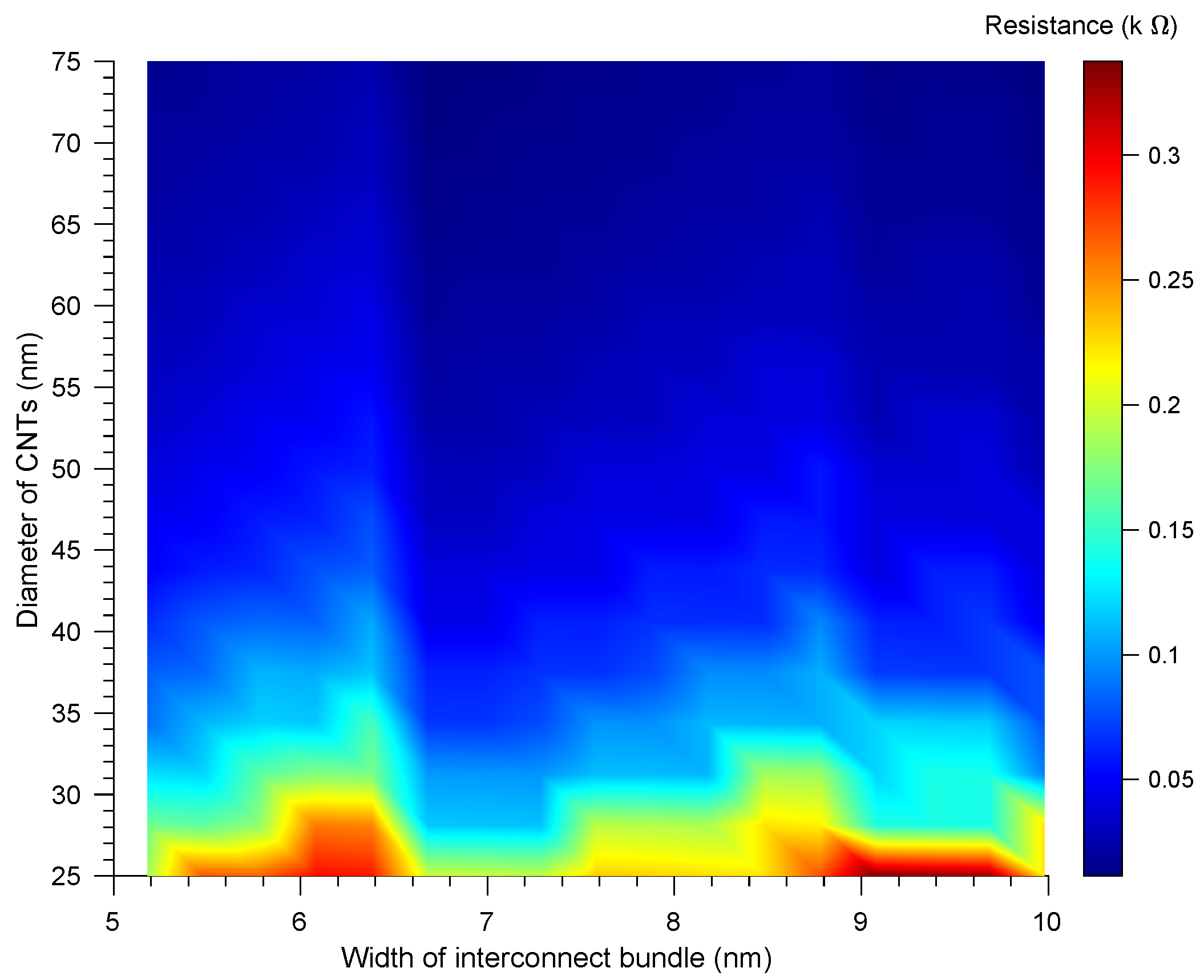
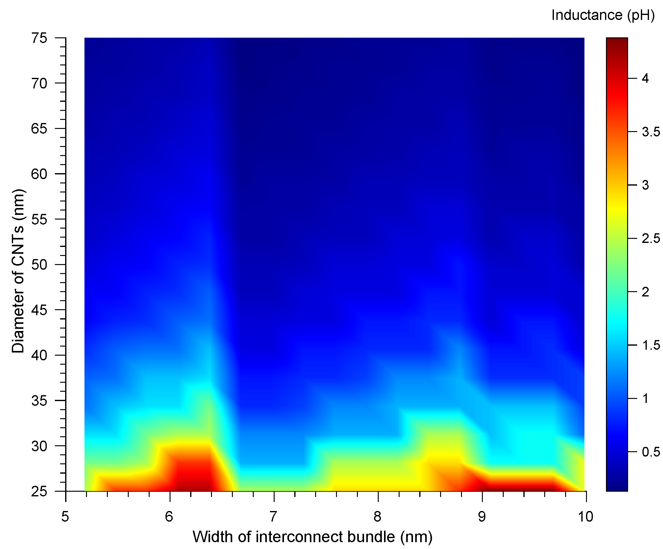
After obtaining the total number of CNTs (both MWCNT and SWCNT) from Section 2, we develop and extract the diameter-controlled elements for the mixed bundle of dimorphic CNTs at different technology nodes in this section. In Figure 2, Figure 3 and Figure 4, the diameter of the MWCNTs is yielded as a function of ‘a’, the diameter of SWCNTs is presumed to be the constant value of 1 nm, and the length of the interconnect and aspect ratio are considered as 100 μm and 2, respectively.
3.1. Resistance in Mixed CNT Bundle
The mathematical approach to determine the equivalent resistance of the mixed bundle is the extraction of the resistance components for isolated CNTs and, eventually, the total resistance of the bundle. To pursue the calculation, we will consider the equivalent single-conductor (ESC) model, where the resistance of the shells of the MWCNTs are in parallel, and adjacent CNTs are also in parallel [24]. According to [25], the quantum resistance () of SWCNTs can be estimated using the conductance , where e is the electron charge with the value of , and is the Planck constant:
On the other hand, in the case of a single-wall nanotube length (l) exceeding the mean free path of electrons (), another resistance () comes up along with the former one, owing to scattering, which can be computed from the following expression:
Finally, the total resistance, emerging from the previous two components of the resistance, for an isolated SWCNT, is denoted by (12):
The lump resistance (), having the quantum or intrinsic resistance from Equation (10), caused by the quantum detainment of electrons in a nano-wire and imperfect metal–nanotube contact resistance (), may vary from a few to several hundreds of kilo-ohms, based on the fabrication process [9,12,26]. The lump resistance for different isolated MWCNTs of the proposed bundle configuration using (13) has been acquired from [4,9,23,24,26,27]:
The per-unit length (p.u.l) scattering resistance () emerges for the length of the nano-wire surpassing the effective mean free path of the electron [24]. The scattering resistance () for different isolated MWCNTs of the proposed bundle configuration is estimated from Equation (14), based on [4,9,26]:
The equivalent resistance of the bundle including both MWCNTs and SWCNTs can be reckoned by the following expression:
The characteristics of resistance (R) depend on both the width of the interconnect wire based on the technology node and the diameter of the used CNTs in the bundle. The simultaneous impact of both factors is observed in Figure 2. It is obvious that the lower resistance for the bundle is attainable by increasing the width of the bundle along with the diameter of the CNTs. Since it is taken into account that all the CNTs in the bundle are in parallel with each other, the increased number of CNTs can be obtained by increasing the width in a given space of the bundle, and can reduce the resistance significantly. Moreover, the increased diameter of the MWCNTs increases the number of shells, which are also in parallel to each other.
3.2. Inductance in Mixed CNT Bundle
To determine the overall inductance for our proposed configuration of the mixed bundle, we will first calculate the inductance for isolated SWCNT and then for the isolated MWCNT, and finally, the equivalent inductance for the entire bundle will be demonstrated, as given in Equation (20). The inductance of the SWCNT consists of two components, which are denoted as kinetic inductance () and magnetic inductance (). Considering the ballistic conduction for a 1D conductor, the kinetic inductance () can be obtained by:
where is the Fermi velocity of an electron with the value of approximately . Since is the function of some constant values, the approximate per-unit length (p.u.l.) value is [28]. On the other hand, the stored energy of carriers in a magnetic field engenders magnetic inductance () in SWCNTs [28] which is approximated by:
with . Now, in the case of MWCNTs, the magnetic inductance for the shell can be approximated by the following expression:
The magnetic and kinetic inductance of the isolated MWCNT in the proposed bundle is calculated using Equations (18) and (19), respectively:
Finally, the overall equivalent inductance of the bundle is estimated in (20), which indicates that the kinetic inductance component of SWCNT exists when the length of the interconnect wire exceeds the electron mean free path:
The inductance of the bundle also exhibits the same phenomena as the resistance does. The behavioral change of the inductance of the bundle, with the width and diameter of the CNTs in the bundle, is depicted in Figure 3. Based on the attained diameter, we estimate the delay of the bundle in Section 4.
3.3. Capacitance in Mixed CNT Bundle
The p.u.l. quantum capacitance for a CNT is estimated in Equation (21) by taking the analogy of the required energy to enclose an extra electron at an acquirable quantum state level beyond the Fermi energy level and effective capacitance. This capacitance comes into notification due to the quantum electrostatic energy stored in the nanotube while carrying the current [28]:
It has already been mentioned that, to estimate the inductance for a isolated SWCNT, that SWCNT must have four conducting channels, and these channels should form a parallel combination [28]. As a result, the equivalent effective quantum capacitance of an isolated SWCNT can be approximated here:
The electrostatic capacitance is expressed in the following expression by considering the SWCNT as a thin wire with the diameter putting, at a distance of ‘y’, away from the ground [28]:
with absolute dielectric permittivity () = . Now, the capacitance for an isolated MWCNT is calculated using the recursive model. It is recommended in [6] that it is mandatory to determine the quantum capacitance of each shell before estimating the effective capacitance of a single MWCNT. The quantum capacitance is basically the estimation of the finite density of electronic states of quantum wire [24].
According to the ESC model of MWCNTs, it can be inferred from [27] that a shell-to-shell mutual capacitance between two adjacent shells of MWCNT is:
where is the diameter of the shell of any isolated MWCNT. At first, in the case of the outermost shell, the equivalent capacitance (), expressed in Equation (26), represents only the quantum capacitance of that shell. As much as we move toward the inner shell, the quantum capacitance of that particular shell makes a parallel combination with the equivalent capacitance (), as shown in expression (28); a series combination of the capacitance of any shell and the mutual capacitance between that shell and previous shell obtained in (27), will continue until reaching the innermost shell.
The electrostatic capacitance demonstrates the potential difference between the ground and the CNT over the ground plane [24]. The p.u.l. electrostatic capacitance can be approximated in (29):
The conglomerate capacitance of the proposed mixed bundle is obtained in (30) by considering the overall effect of the SWCNTs and MWCNTs in the bundle. To estimate this, we considered the effect of electrostatic capacitance of MWCNTs over the ground plane on the effective capacitance in series:
Unlike the resistance and inductance, capacitance shows a descending behavior, with a lower diameter of CNTs in the bundle. We can also notice, from Figure 4, that capacitance decreases further in higher-technology nodes. The reason behind this phenomenon is that the capacitance components rising from parallel CNTs magnify the equivalent capacitance in the bundle.
4. Simulation Results
This section illustrates the performance comparison of a squarely packed bundle of dimorphic MWCNTs and that of mixed CNTs to exploit the feature of using mixed CNTs in the interconnect bundle. To observe the performance in terms of propagation delay, we simulate the Kahng’s model, obtained from earlier work [13], using the extracted equivalent value of and the optimized dimensions of CNTs in Section 3. Having the value of our model, we validate the extracted conductance, inductance and capacitance rising in our configuration by comparing them with those in the previously discussed mixed CNT model in [18]. Subsequently, we assess the performance of the proposed configuration in terms of crosstalk delay, excerpted from [4], using the optimized size of particular CNTs and extracted in Section 3, and the number of CNTs in Section 2.
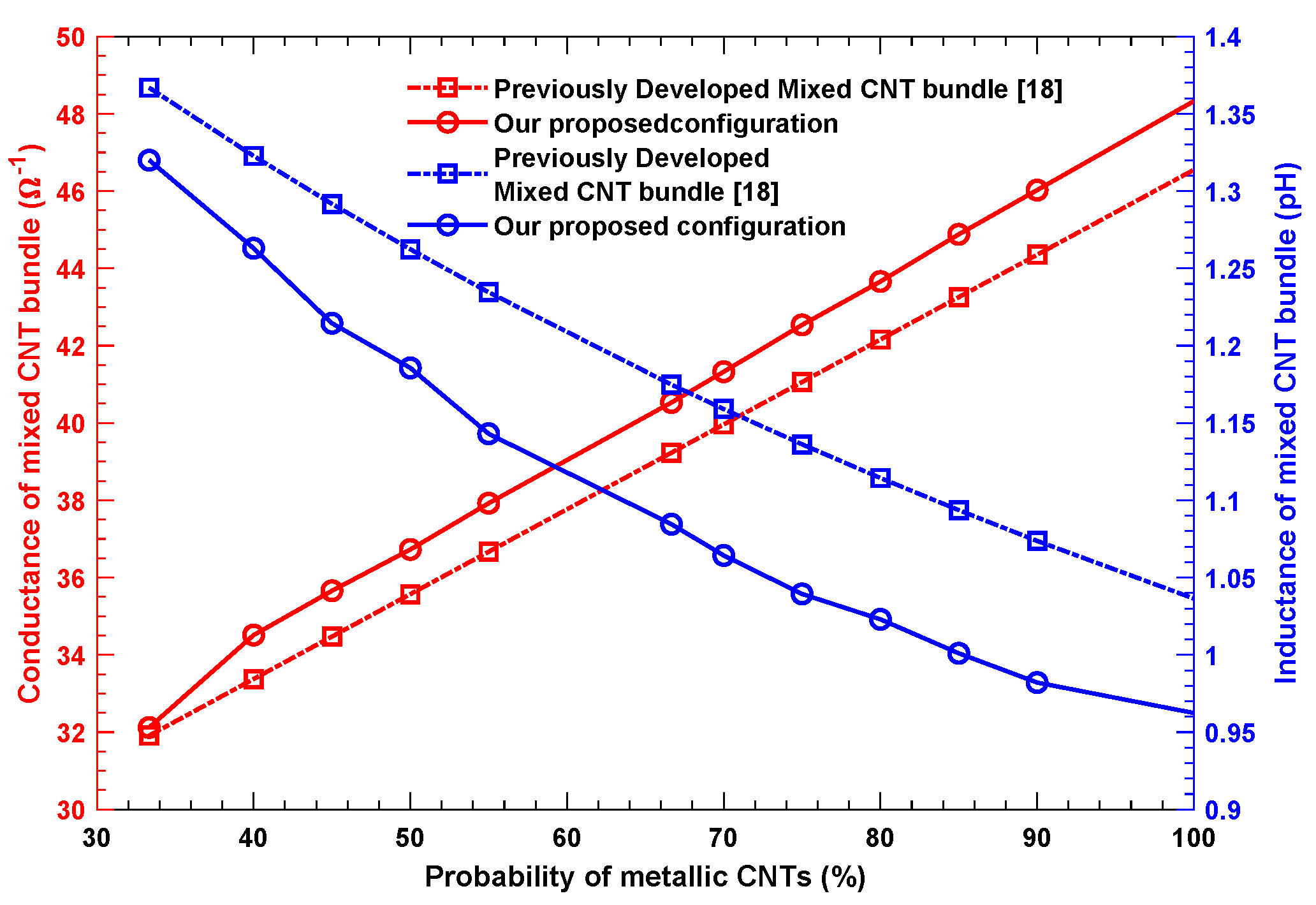
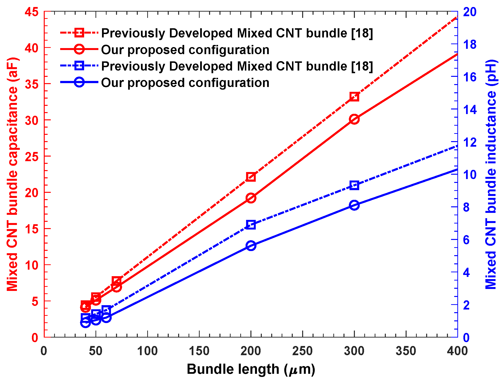
To validate the value of the proposed model, the conductance and inductance of the mixed CNT bundle is observed by varying the probability of metallic CNT (%) using Equation (1). We observe, from Figure 5, that the conductance of our mixed CNT bundle configuration varies proportionally with the percentage of metallic CNTs in the bundle. It can be deduced from expression (1) that the number of channels per shell increases with an increase in the percentage of metallic CNTs, which, in turn, reduces the resistance and increases the conductance of the bundle. As our proposed configuration is densely packed and geometrically organized, its capacity to hold a noticeably higher number of CNTs in the bundle makes the conductance of our configuration, as depicted in Figure 5, much higher than that of the mixed CNT bundle in [18]. For the same reason, our proposed configuration comes up with a lower inductance than the previous mixed CNT models in both Figure 5 and Figure 6. Figure 6, meanwhile, demonstrates that the capacitance of the proposed model increases with increasing interconnect lengths, though our configuration still sustains better performance by generating lower capacitances. In this circumstance, we can infer that by increasing the percentage of metallic CNTs and delimiting the interconnect length, we can reduce the extracted parameter and, eventually, the delay.
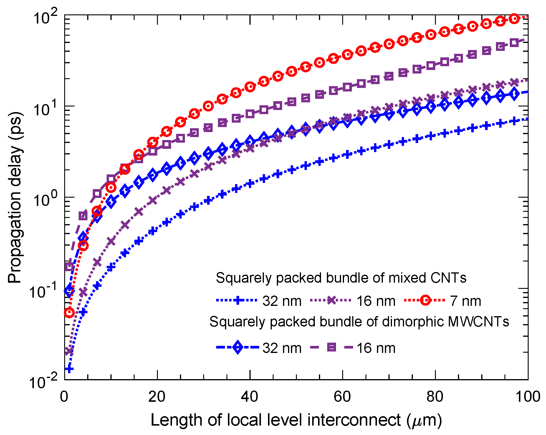
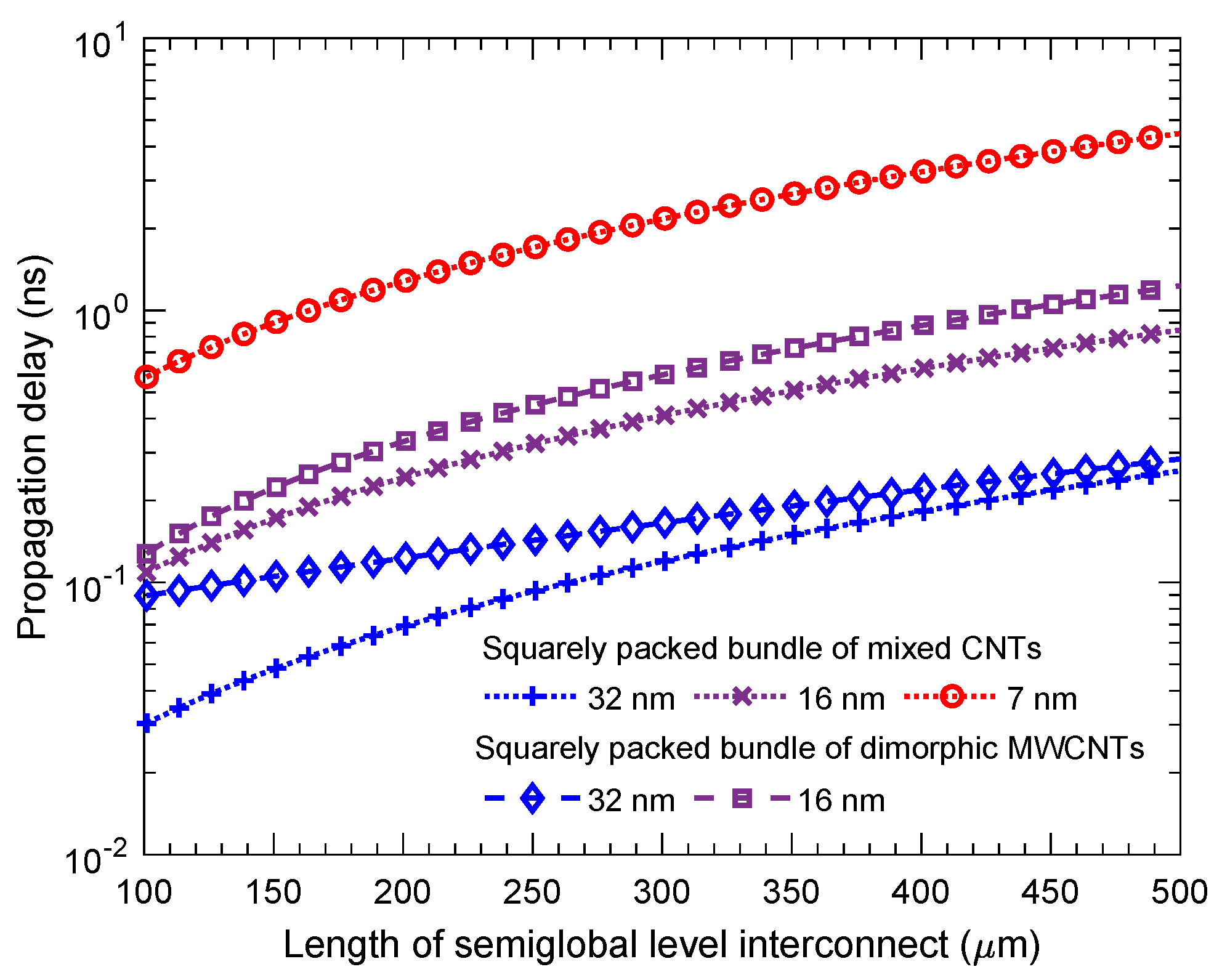
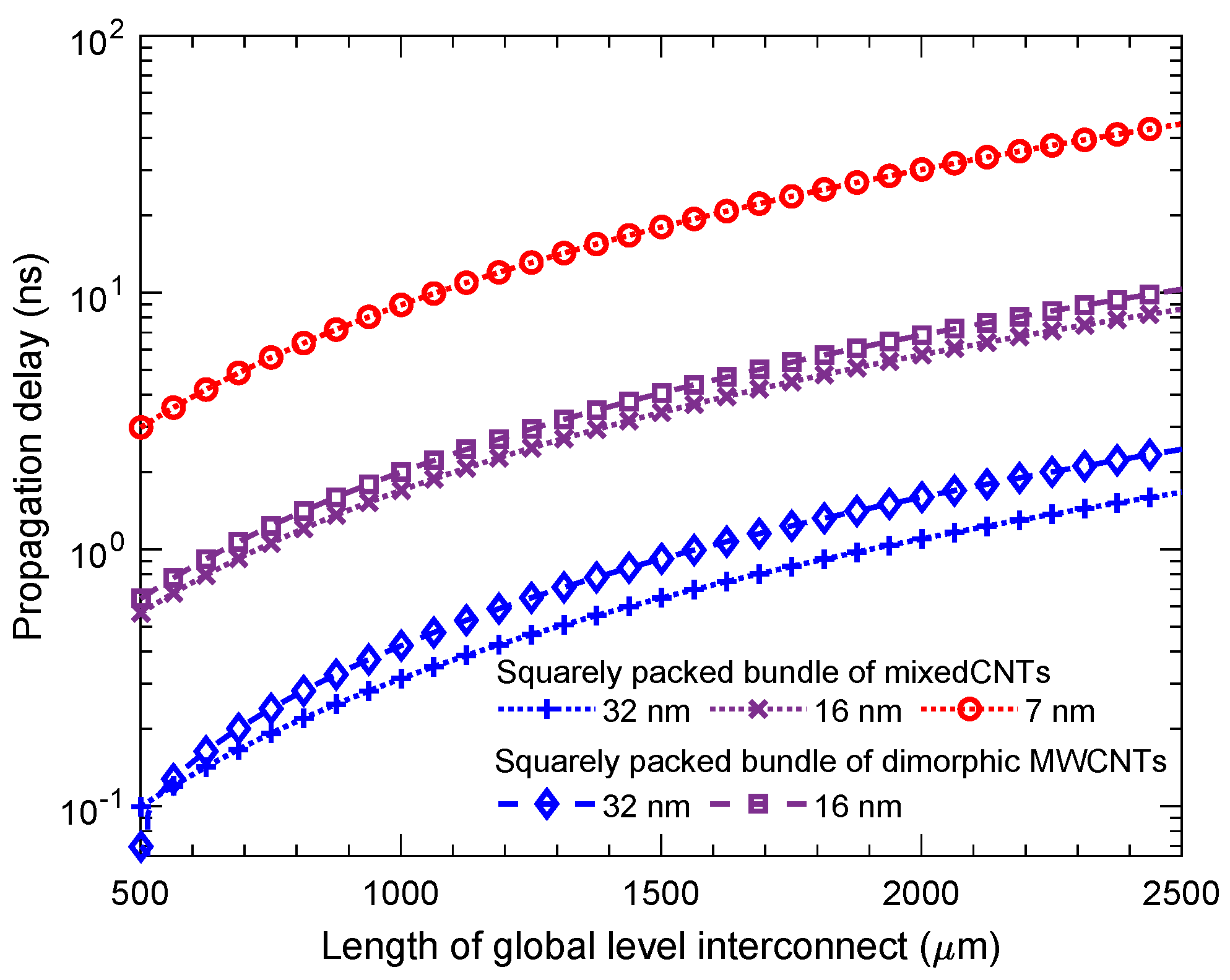
It is demonstrable from Figure 7, Figure 8 and Figure 9 that our proposed configuration yields a lower propagation delay than the preceding configuration in [17] does. It is conspicuous, from Table 1. that we can increase the number of CNTs without distorting the overall configuration of the squarely packed bundle using the proposed approach. As a consequence, the resistance and inductance decreases while the capacitance increases for any specific technology node. Finally, the overall impact decreases the propagation delay for the squarely packed bundle of mixed CNTs, which is represented in the Figure 7, Figure 8 and Figure 9 for the local, semiglobal, and global levels, respectively. However, the preceding squarely packed bundle configuration does not seem suitable for 7- technology nodes, because of the unavailability of space to accommodate CNTs of various sizes. Hence, the simulation illustrations don not include the delay of a squarely packed bundle of dimorphic MWCNTs for 7- technology. In comparison with [18], the unique contribution of our proposed configuration is the feasibility for 32-, 16-, and 7- technology nodes, along with performance enhancements.
The crosstalk delay, basically, arises from the capacitance formed between the CNTs from different bundles, while it is considered that all CNTs in the bundles are in parallel [4]. The inter-bundle capacitance, the function of spacing between the the centers of two adjacent CNTs, the average diameter of the adjacent CNTs, and the relative permittivity based on the level of interconnect length, is estimated by Equation (31), where is used as the diameter because we placed MWCNTs on the edge of the bundle to reduce the overall crosstalk impact, having been motivated by previous works [6,9]:
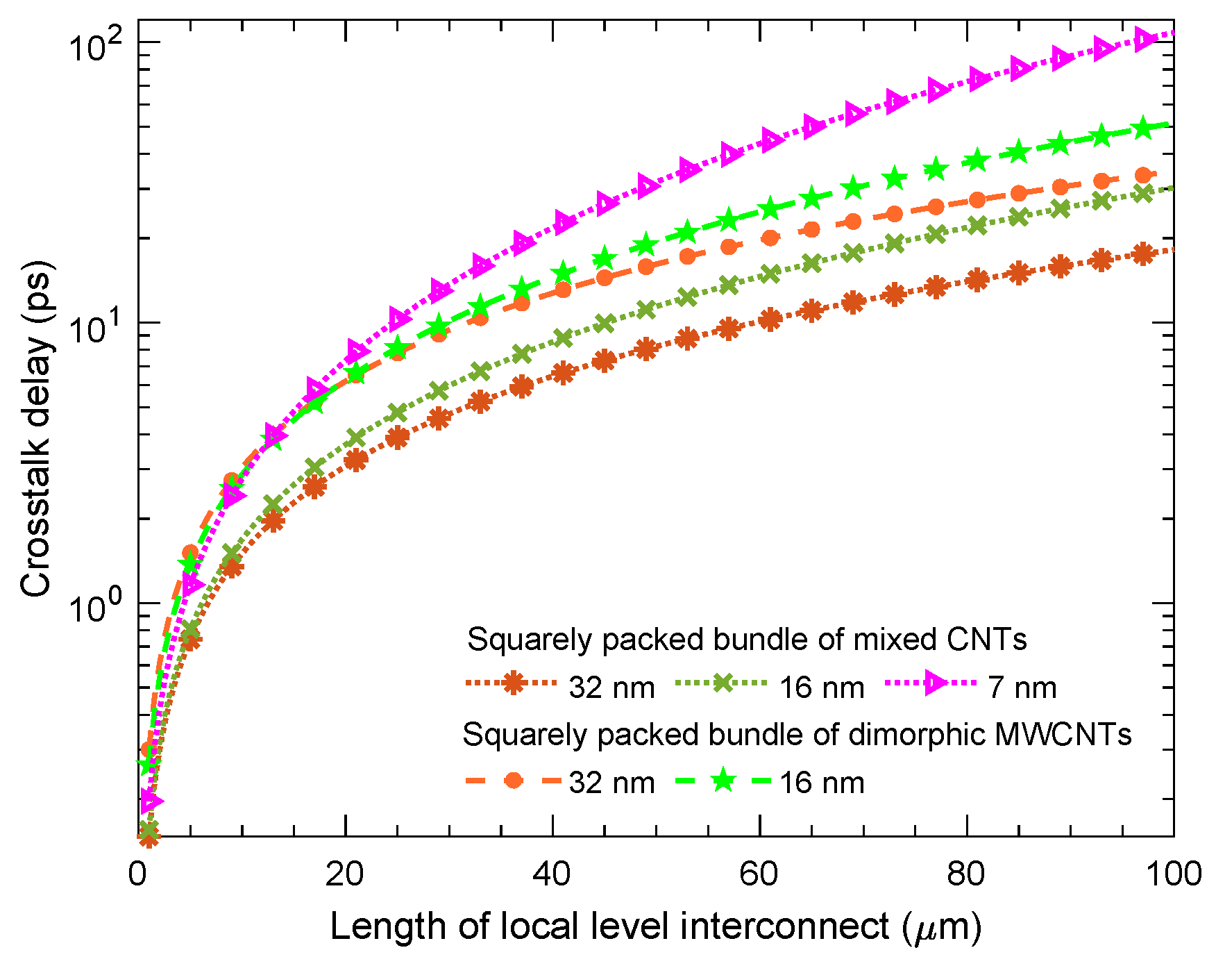
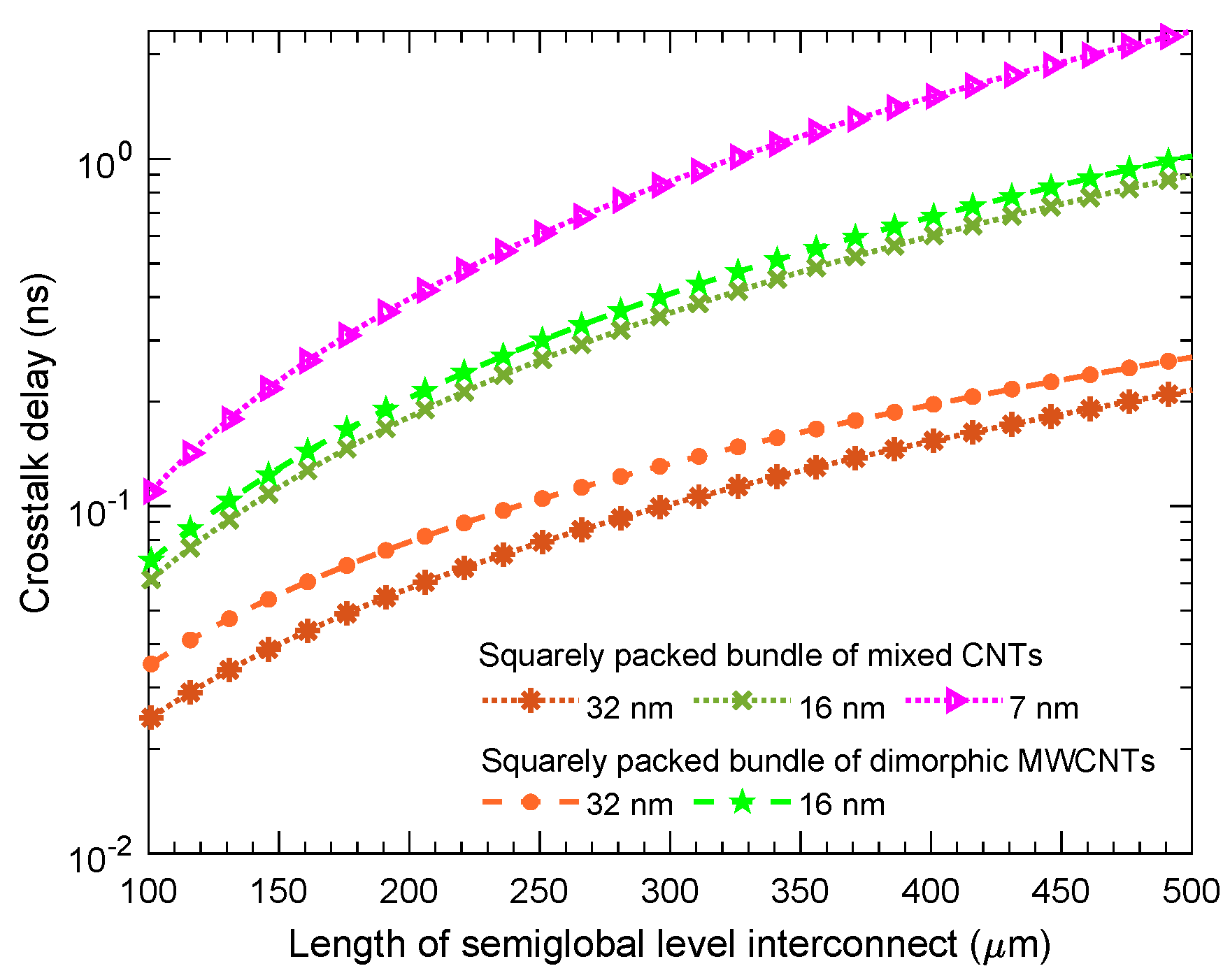
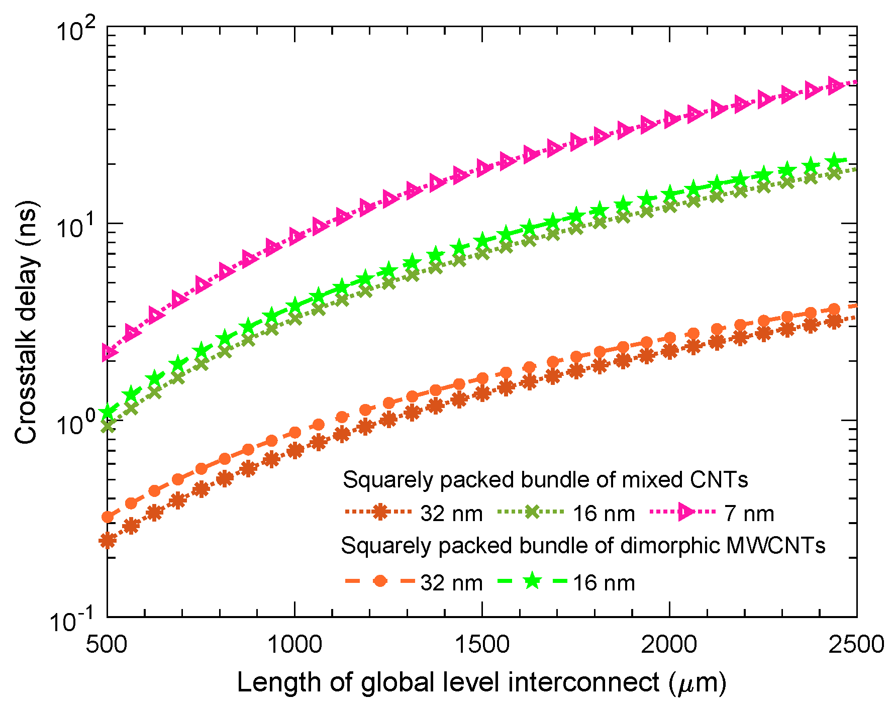
Eventually, the crosstalk performance of our proposed configuration is depicted in Figure 10, Figure 11 and Figure 12 for local-, semiglobal-, and global-level interconnects by comparing with the preceding configuration from [17]. It is noticeable from Figure 11 that the crosstalk performance of the proposed configuration is substantial for both the 32- and 16- technology nodes. On the other hand, Figure 11 illustrates significant crosstalk performance betterment in the 32- technology node, compared with that in the 16- technology node. In the case of the global-level interconnect, the amount of crosstalk delay performance enhancement of our proposed configuration for both 32- and 16- technology nodes is almost the same, as is illustrated in Figure 12. It is also demonstrable that our proposed configuration is appropriate for 7- technology nodes.
5. Conclusions
A modified configuration of the squarely packed bundle of mixed CNTs is presented to assure the high speed VLSI interconnect with less area possession. By proposing this configuration, the simultaneous applicability of both MWCNTs and SWCNTs for scaled interconnects in future VLSI-integrated circuits is analyzed abstractly. The propagation delay and crosstalk delay performance are extracted and analyzed using an model and a delay model. As a result, it exhibits the transcendence of squarely packed bundles of mixed CNTs for local-, semiglobal-, and global-level interconnects at 32-, 16-, and 7- technology nodes. In this approach, CNTs with only two different sizes are used. In the upcoming endeavor, our intention is to advance the work by adding the CNTs with various sizes to make the configuration more convenient in terms of fabrication process.
Author Contributions
Conceptualization, A.B.A.; methodology, A.B.A.; software, A.B.A.; validation, A.B.A.; formal analysis, A.B.A.; investigation, A.B.A.; resources, S.M.S.; data curation, A.B.A.; writing—original draft preparation, A.B.A.; writing—review and editing, A.B.A.; visualization, A.B.A.; supervision, M.S.U.; project administration, M.S.U.; funding acquisition, M.S.U. All authors have read and agreed to the published version of the manuscript.
Funding
This research received no external funding.
Institutional Review Board Statement
Not applicable.
Informed Consent Statement
Not applicable.
Data Availability Statement
Not applicable.
Conflicts of Interest
The authors declare no conflict of interest.
References
- Li, H.; Yin, W.Y.; Banerjee, K.; Mao, J.F. Circuit modeling and performance analysis of multi-walled carbon nanotube interconnects. IEEE Trans. Electron Devices 2008, 55, 1328–1337. [Google Scholar] [CrossRef] [Green Version]
- Kabir, M.S. Controlled Growth of a Nanostructure on a Substrate, and Electron Emission Devices Based on the Same. U.S. Patent 7,977,761, 12 July 2011. [Google Scholar]
- Liew, K.; Wong, C.; He, X.; Tan, M. Thermal stability of single and multi-walled carbon nanotubes. Phys. Rev. B 2005, 71, 075424. [Google Scholar] [CrossRef]
- Kaushik, B.K.; Majumder, M.K. Carbon Nanotube Based VLSI Interconnects: Analysis and Design; Springer: Berlin/Heidelberg, Germany, 2015. [Google Scholar]
- Pu, S.; Yin, W.; Mao, J.; Liu, Q.H. Crosstalk Prediction of Single- and Double-Walled Carbon-Nanotube (SWCNT/DWCNT) Bundle Interconnects. IEEE Trans. Electron Devices 2009, 56, 560–568. [Google Scholar] [CrossRef]
- Subash, S.; Kolar, J.; Chowdhury, M.H. A new spatially rearranged bundle of mixed carbon nanotubes as VLSI interconnection. IEEE Trans. Nanotechnol. 2011, 12, 3–12. [Google Scholar] [CrossRef]
- Kim, S.; Kulkarni, D.D.; Rykaczewski, K.; Henry, M.; Tsukruk, V.V.; Fedorov, A.G. Fabrication of an ultralow-resistance ohmic contact to MWCNT–metal interconnect using graphitic carbon by electron beam-induced deposition (EBID). IEEE Trans. Nanotechnol. 2012, 11, 1223–1230. [Google Scholar] [CrossRef]
- Amin, A.B.; Ullah, M.S. Mathematical Framework of Tetramorphic MWCNT Configuration for VLSI Interconnect. IEEE Trans. Nanotechnol. 2020, 19, 749–759. [Google Scholar] [CrossRef]
- Majumder, M.K.; Kaushik, B.K.; Manhas, S.K. Analysis of delay and dynamic crosstalk in bundled carbon nanotube interconnects. IEEE Trans. Electromagn. Compat. 2014, 56, 1666–1673. [Google Scholar] [CrossRef]
- Rai, M.K.; Garg, H.; Kaushik, B. Temperature-dependent modeling and crosstalk analysis in mixed carbon nanotube bundle interconnects. J. Electron. Mater. 2017, 46, 5324–5337. [Google Scholar] [CrossRef]
- Sharma, M.; Rai, M.K.; Khanna, R. Temperature-dependent crosstalk and frequency spectrum analyses in adjacent interconnects of a mixed CNT bundle. J. Comput. Electron. 2020, 19, 177–190. [Google Scholar] [CrossRef]
- Sandha, K.S.; Thakur, A. Comparative Analysis of Mixed CNTs and MWCNTs as VLSI Interconnects for Deep Sub-micron Technology Nodes. J. Electron. Mater. 2019, 48, 2543–2554. [Google Scholar] [CrossRef]
- Kahng, A.B.; Muddu, S. An analytical delay model for RLC interconnects. IEEE Trans. Comput.-Aided Des. Integr. Circuits Syst. 1997, 16, 1507–1514. [Google Scholar] [CrossRef] [Green Version]
- Ullah, M.S.; Chowdhury, M.H. Analytical models of high-speed RLC interconnect delay for complex and real poles. IEEE Trans. Very Large Scale Integr. (VLSI) Syst. 2017, 25, 1831–1841. [Google Scholar] [CrossRef]
- Sanaullah, M.; Chowdhury, M.H. Analysis of RLC interconnect delay model using second order approximation. In Proceedings of the 2014 IEEE International Symposium on Circuits and Systems (ISCAS), Melbourne, VIC, Australia, 1–5 June 2014; pp. 2756–2759. [Google Scholar] [CrossRef]
- Sanaullah, M.; Chowdhury, M.H. A new real pole delay model for RLC interconnect using second order approximation. In Proceedings of the 2014 IEEE 57th International Midwest Symposium on Circuits and Systems (MWSCAS), College Station, TX, USA, 3–6 August 2014; pp. 238–241. [Google Scholar] [CrossRef]
- Amin, A.B.; Ullah, M.S. Performance Analysis of Squarely Packed Dimorphic MWCNT Bundle for High Speed VLSI Interconnect. In Proceedings of the 2020 IEEE Canadian Conference on Electrical and Computer Engineering (CCECE), London, ON, Canada, 30 August–2 September 2020; pp. 1–6. [Google Scholar] [CrossRef]
- Subash, S.; Chowdhury, M.H. Mixed carbon nanotube bundles for interconnect applications. Int. J. Electron. 2009, 96, 657–671. [Google Scholar] [CrossRef]
- Li, H.; Lu, W.; Li, J.; Bai, X.; Gu, C. Multichannel ballistic transport in multiwall carbon nanotubes. Phys. Rev. Lett. 2005, 95, 086601. [Google Scholar] [CrossRef] [Green Version]
- Naeemi, A.; Meindl, J.D. Compact physical models for multiwall carbon-nanotube interconnects. IEEE Electron Device Lett. 2006, 27, 338–340. [Google Scholar] [CrossRef]
- Amin, A.B.; Ullah, M.S. Performance Analysis of Squarely Packed Polymorphic SWCNT Interconnect. In Proceedings of the 2019 IEEE 10th Annual Ubiquitous Computing, Electronics Mobile Communication Conference (UEMCON), New York, NY, USA, 10–12 October 2019; pp. 1199–1203. [Google Scholar] [CrossRef]
- Naeemi, A.; Meindl, J.D. Physical modeling of temperature coefficient of resistance for single-and multi-wall carbon nanotube interconnects. IEEE Electron Device Lett. 2007, 28, 135–138. [Google Scholar] [CrossRef]
- Das, D.; Rahaman, H. Analysis of crosstalk in single-and multiwall carbon nanotube interconnects and its impact on gate oxide reliability. IEEE Trans. Nanotechnol. 2011, 10, 1362–1370. [Google Scholar] [CrossRef]
- Majumder, M.K.; Das, P.K.; Kaushik, B.K. Delay and crosstalk reliability issues in mixed MWCNT bundle interconnects. Microelectron. Reliab. 2014, 54, 2570–2577. [Google Scholar] [CrossRef]
- Srivastava, N.; Li, H.; Kreupl, F.; Banerjee, K. On the applicability of single-walled carbon nanotubes as VLSI interconnects. IEEE Trans. Nanotechnol. 2009, 8, 542–559. [Google Scholar] [CrossRef]
- Sahoo, M.; Ghosal, P.; Rahaman, H. Modeling and analysis of crosstalk induced effects in multiwalled carbon nanotube bundle interconnects: An ABCD parameter-based approach. IEEE Trans. Nanotechnol. 2015, 14, 259–274. [Google Scholar] [CrossRef]
- Sarto, M.S.; Tamburrano, A. Single-conductor transmission-line model of multiwall carbon nanotubes. IEEE Trans. Nanotechnol. 2009, 9, 82–92. [Google Scholar] [CrossRef]
- Banerjee, K.; Srivastava, N. Are carbon nanotubes the future of VLSI interconnections? In Proceedings of the 43rd annual Design Automation Conference, San Francisco, CA, USA, 24–28 July 2006; pp. 809–814. [Google Scholar]
Figure 1.
(a,b) In both architectures, the size of the larger MWCNTs are the same. The main modification happened in the introduced configuration by means of smaller MWCNTs replaced by a bunch of SWCNTs with the same predefined diameter, according to the space available based on the technology nodes.

Figure 2.
Synchronal variation of resistance of the squarely packed bundle of mixed CNTs from altering the width of the bundle and the diameter of the CNTs.
Figure 2.
Synchronal variation of resistance of the squarely packed bundle of mixed CNTs from altering the width of the bundle and the diameter of the CNTs.

Figure 3.
Concurrent extraction of inductance of the squarely packed bundle of mixed CNTs by varying the width of the bundle and the diameter of the CNTs.
Figure 3.
Concurrent extraction of inductance of the squarely packed bundle of mixed CNTs by varying the width of the bundle and the diameter of the CNTs.

Figure 4.
Contemporaneous denouement of capacitance of the squarely packed bundle of mixed CNTs by varying the width of the bundle and the diameter of CNTs.
Figure 4.
Contemporaneous denouement of capacitance of the squarely packed bundle of mixed CNTs by varying the width of the bundle and the diameter of CNTs.

Figure 5.
Impact of increasing metallic CNTs on the conductance and inductance and comparison of the results of the proposed configuration and the earlier mixed CNT bundle configuration. Overall conductance and inductance of the mixed CNT bundle is obtained, considering the interconnect length of 40 .

Figure 6.
Findings of overall bundle inductance (L) and capacitance (C) for different interconnect lengths to observe the comparative parameter illustration of the proposed configuration and the previous model by considering that of the CNTs are metallic in the bundle.
Figure 6.
Findings of overall bundle inductance (L) and capacitance (C) for different interconnect lengths to observe the comparative parameter illustration of the proposed configuration and the previous model by considering that of the CNTs are metallic in the bundle.

Figure 7.
Comparison of delay performance of a squarely packed bundle of mixed CNTs and that of dimorphic MWCNTs for local-level interconnect lengths. The size and number of accommodated CNTs for different technology nodes are mentioned in Table 1.
Figure 7.
Comparison of delay performance of a squarely packed bundle of mixed CNTs and that of dimorphic MWCNTs for local-level interconnect lengths. The size and number of accommodated CNTs for different technology nodes are mentioned in Table 1.

Figure 8.
Illustration of comparative delay performance of a squarely packed bundle of mixed CNTs and that of dimorphic MWCNTs for semiglobal-level interconnect lengths. The size and number of accommodated CNTs for different technology nodes are mentioned in Table 1.
Figure 8.
Illustration of comparative delay performance of a squarely packed bundle of mixed CNTs and that of dimorphic MWCNTs for semiglobal-level interconnect lengths. The size and number of accommodated CNTs for different technology nodes are mentioned in Table 1.

Figure 9.
Demonstration of comparison between the propagation delay performance of a squarely packed bundle of mixed CNTs and that of dimorphic MWCNTs for global-level interconnect lengths. The size and number of accommodated CNTs for different technology nodes are mentioned in Table 1.
Figure 9.
Demonstration of comparison between the propagation delay performance of a squarely packed bundle of mixed CNTs and that of dimorphic MWCNTs for global-level interconnect lengths. The size and number of accommodated CNTs for different technology nodes are mentioned in Table 1.

Figure 10.
Comparative exhibition of the crosstalk delay of the proposed and previously developed bundle configurations for different technology nodes at local-level interconnect lengths. The dimension of the used CNTs are the same as those used in the simulation for obtaining propagation delays at the local level.

Figure 11.
Comparative analysis of the crosstalk delay of the proposed and previously developed bundle configurations for different technology nodes at semiglobal-level interconnect lengths. The dimension of the used CNTs are the same as those used in the simulation for obtaining propagation delays at the semiglobal level.

Figure 12.
Comparative illustration of the crosstalk delay of the proposed and previously developed bundle configurations for different technology nodes at global-level interconnect lengths. The diameter and number of the used CNTs are the same as those used in the simulation for obtaining propagation delays at the global level.


Table 1.
Diameter and number of pertinent CNTs accommodated in the bundle during simulation to obtain propagation delay and crosstalk delay.
Table 1.
Diameter and number of pertinent CNTs accommodated in the bundle during simulation to obtain propagation delay and crosstalk delay.
| Interconnect Length (m) | Technology Node (nm) | Squarely Packed Dimorphic | Squarely Packed Mixed | ||||||
|---|---|---|---|---|---|---|---|---|---|
(nm) | (nm) | (nm) | (nm) | ||||||
| Local (0–100) | 32 | 10 | 32 | 4.31 | 21 | 10 | 21 | 1 | 96 |
| 16 | 8.5 | 8 | 3.72 | 3 | 8.5 | 8 | 1 | 15 | |
| 7 | - | - | - | - | 4.5 | 3 | 1 | 8 | |
| Semiglobal (101–500) | 32 | 10 | 32 | 4.31 | 21 | 10 | 21 | 1 | 96 |
| 16 | 8.5 | 8 | 3.72 | 3 | 8.5 | 8 | 1 | 15 | |
| 7 | - | - | - | - | 4.5 | 3 | 1 | 8 | |
| Global (501–2500) | 32 | 10 | 48 | 4.31 | 33 | 10 | 33 | 1 | 160 |
| 16 | 8.5 | 14 | 3.72 | 6 | 8.5 | 12 | 1 | 25 | |
| 7 | - | - | - | - | 4.5 | 12 | 1 | 5 | |
Publisher’s Note: MDPI stays neutral with regard to jurisdictional claims in published maps and institutional affiliations. |
© 2022 by the authors. Licensee MDPI, Basel, Switzerland. This article is an open access article distributed under the terms and conditions of the Creative Commons Attribution (CC BY) license (https://creativecommons.org/licenses/by/4.0/).
Share and Cite
MDPI and ACS Style
Amin, A.B.; Shakil, S.M.; Ullah, M.S. A Theoretical Modeling of Adaptive Mixed CNT Bundles for High-Speed VLSI Interconnect Design. Crystals 2022, 12, 186. https://0-doi-org.brum.beds.ac.uk/10.3390/cryst12020186
AMA Style
Amin AB, Shakil SM, Ullah MS. A Theoretical Modeling of Adaptive Mixed CNT Bundles for High-Speed VLSI Interconnect Design. Crystals. 2022; 12(2):186. https://0-doi-org.brum.beds.ac.uk/10.3390/cryst12020186
Chicago/Turabian StyleAmin, Abu Bony, Syed Muhammad Shakil, and Muhammad Sana Ullah. 2022. "A Theoretical Modeling of Adaptive Mixed CNT Bundles for High-Speed VLSI Interconnect Design" Crystals 12, no. 2: 186. https://0-doi-org.brum.beds.ac.uk/10.3390/cryst12020186
Note that from the first issue of 2016, this journal uses article numbers instead of page numbers. See further details here.