
Review of Silicon Carbide Processing for Power MOSFET

 ,
, 
Abstract
:1. Introduction
1.1. SiC Materials Properties
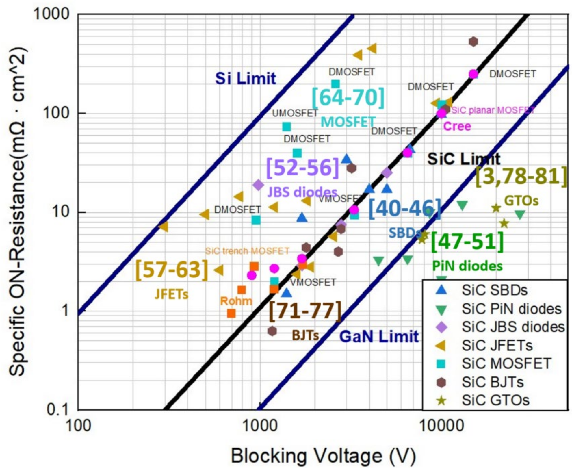
1.2. SiC Power Devices
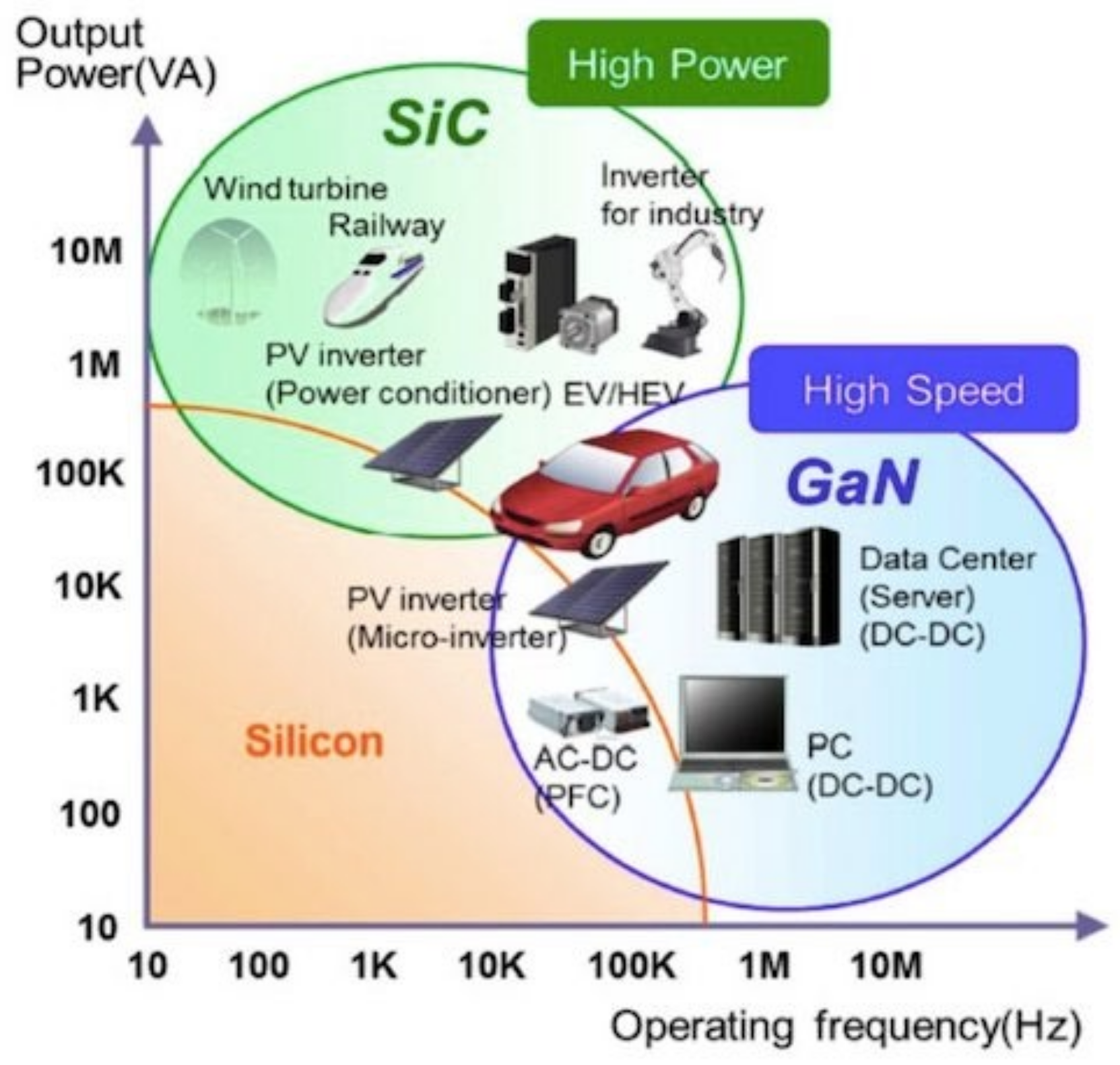
1.3. SiC Applications
2. SiC Critical Step
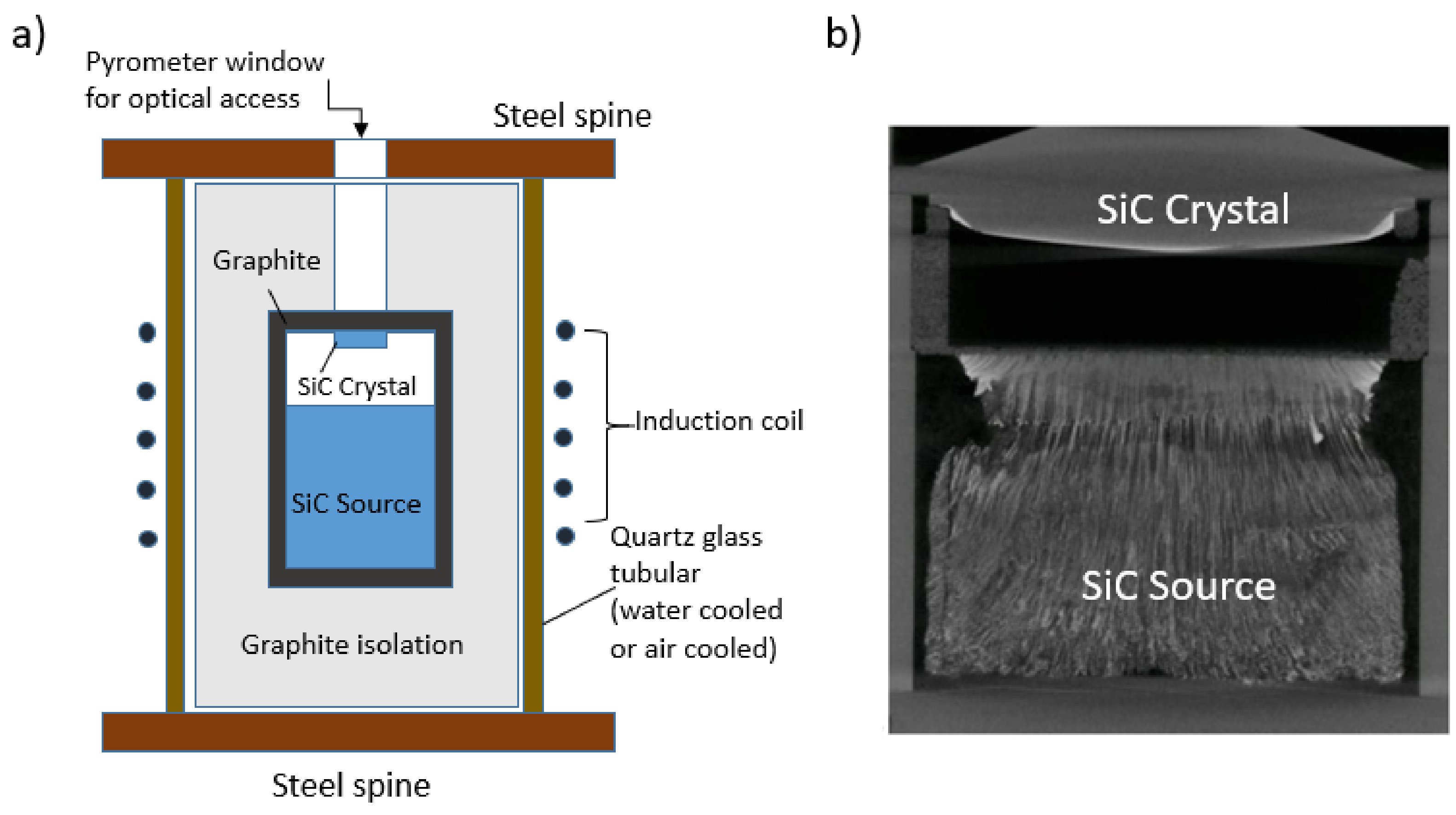
2.1. SiC Substrate
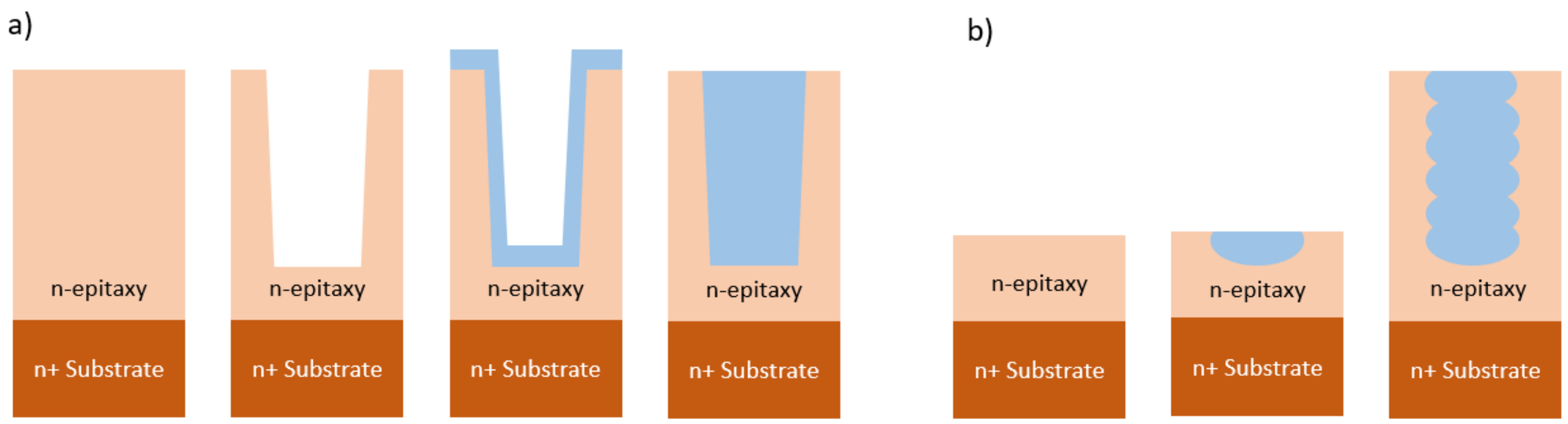
2.2. SiC Epitaxy
2.3. Ion Implant
2.4. Oxidation
3. SiC MOSFETs
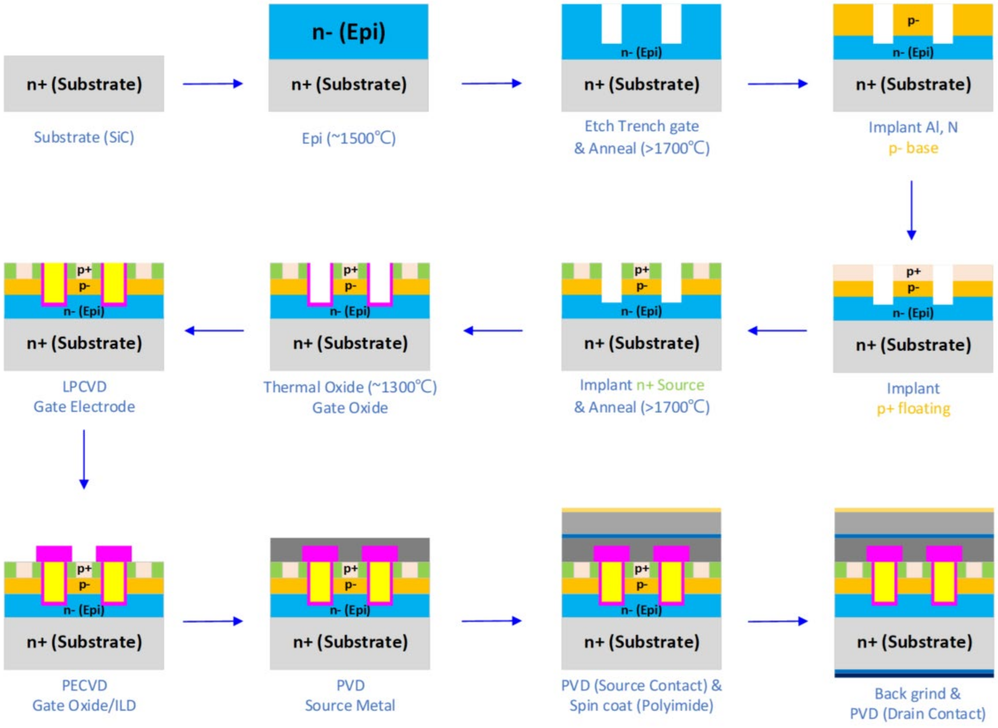
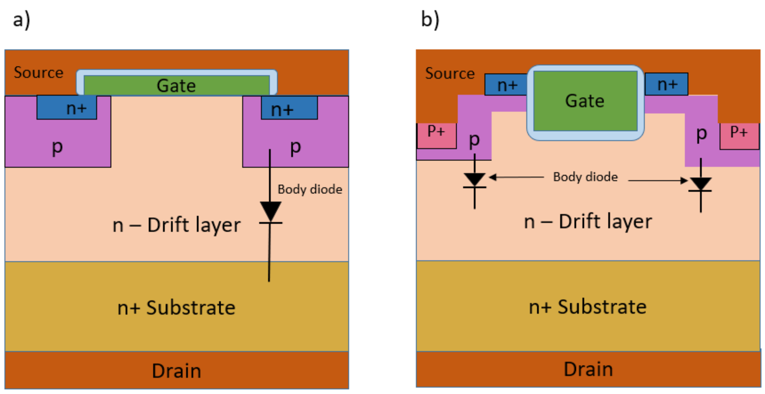
3.1. Planar and Trench MOSFETs
3.2. Superjunction MOSFETs
4. Device Reliability
4.1. Threshold Voltage Degradation
4.2. Gate Oxide Degradation
4.3. Body Diode Degradation
5. Conclusions
Author Contributions
Funding
Institutional Review Board Statement
Informed Consent Statement
Data Availability Statement
Acknowledgments
Conflicts of Interest
References
- Kassakian, J.G.; Jahns, T.M. Evolving and emerging applications of power electronics in systems. IEEE J. Emerg. Sel. Top. Power Electron. 2013, 1, 47–58. [Google Scholar] [CrossRef]
- Van Wyk, J.D.; Lee, F.C. On a future for power electronics. IEEE J. Emerg. Sel. Top. Power Electron. 2013, 1, 59–72. [Google Scholar] [CrossRef]
- Palmour, J.W. Silicon carbide power device development for industrial markets. In Proceedings of the 2014 IEEE International Electron Devices Meeting, San Francisco, CA, USA, 15–17 December 2014; pp. 1.1.1–1.1.8. [Google Scholar]
- Millán, J.; Godignon, P.; Perpiñà, X.; Pérez-Tomás, A.; Rebollo, J. A Survey of Wide Bandgap Power Semiconductor Devices. IEEE Trans. Power Electron. 2014, 29, 2155–2163. [Google Scholar] [CrossRef]
- Hertz, J. 2021 Starts With a Hot Streak for Silicon Carbide. 2021. Available online: https://www.allaboutcircuits.com/news/2021-starts-with-a-hot-streak-for-silicon-carbide (accessed on 12 October 2021).
- Biela, J.; Schweizer, M.; Waffler, S.; Kolar, J.W. SiC versus Si—Evaluation of Potentials for Performance Improvement of Inverter and DC–DC Converter Systems by SiC Power Semiconductors. IEEE Trans. Ind. Electron. 2011, 58, 2872–2882. [Google Scholar] [CrossRef]
- Chow, T.-S. SiC and GaN High voltage Power switching devices. Mater. Sci. Forum 2000, 338–342, 1155–1160. [Google Scholar] [CrossRef]
- Nakamura, T.; Sasagawa, M.; Nakano, Y.; Otsuka, T.; Miura, M. Large current SiC power devices for automobile applications. In Proceedings of the 2010 International Power Electronics Conference—ECCE ASIA, Sapporo, Japan, 21–24 June 2010; pp. 1023–1026. [Google Scholar]
- Kimoto, T.; Cooper, J.A. Fundamentals of Silicon Carbide Technology: Growth, Characterization, Devices and Applications; John Wiley & Sons: Hoboken, NJ, USA, 2014; Available online: https://0-onlinelibrary-wiley-com.brum.beds.ac.uk/doi/book/10.1002/9781118313534 (accessed on 5 October 2021).
- Saddow, S.E.; Agarwal, A.K. Advances in Silicon Carbide Processing and Applications; Artech House: Boston, MA, USA, 2004. [Google Scholar]
- Kumar, V.; Kumar, S.; Maan, A.S.; Akhtar, J. Interface improvement of epitaxial 4H-SiC based Schottky didoes by selective heavy ion irradiation. Available online: https://0-link-springer-com.brum.beds.ac.uk/article/10.1007/s13204-020-01608-3 (accessed on 5 October 2021).
- Zhang, Y. Comparison between competing requirements of GaN and SiC family of power switching devices. IOP Conf. Ser. Mater. Sci. Eng. 2020, 738, 012004. [Google Scholar] [CrossRef]
- Berzelius, J.J. Untersuchungen über die Flussspathsäure und deren merkwürdigsten Verbindungen. Ann. Der Phys. 1824, 80, 1–22. [Google Scholar] [CrossRef] [Green Version]
- Cheung, R. Silicon Carbide Microelectromechanical Systems for Harsh Environments; World Scientific: Singapore, 2006. [Google Scholar]
- Gachovska, T.K.; Hudgins, J.L. SiC and GaN Power Semiconductor Devices. In Power Electronics Handbook; Elsevier: Amsterdam, The Netherlands, 2018; pp. 95–155. [Google Scholar]
- Jian, J.; Sun, J. A Review of Recent Progress on Silicon Carbide for Photoelectrochemical Water Splitting. Sol. RRL 2020, 4, 2000111. [Google Scholar] [CrossRef] [Green Version]
- Palmour, J.; Singh, R.; Glass, R.; Kordina, O.; Carter, C. Silicon carbide for power devices. In Proceedings of the 9th International Symposium on Power Semiconductor Devices and IC’s, Weimar, Germany, 26–29 May 1997; pp. 25–32. [Google Scholar]
- Itoh, A.; Akita, H.; Kimoto, T.; Matsunami, H. High-quality 4H-SiC homoepitaxial layers grown by step-controlled epitaxy. Appl. Phys. Lett. 1994, 65, 1400–1402. [Google Scholar] [CrossRef]
- Konstantinov, A.; Wahab, Q.; Nordell, N.; Lindefelt, U. Ionization rates and critical fields in 4H silicon carbide. Appl. Phys. Lett. 1997, 71, 90–92. [Google Scholar] [CrossRef]
- Wijesundara, M.; Azevedo, R. Silicon Carbide Microsystems for Harsh Environments; Springer Science & Business Media: Berlin/Heidelberg, Germany, 2011; Volume 22. [Google Scholar]
- Neudeck, P.G. Silicon Carbide Technology. The VLSI Handbook, 20061800. 2006. Available online: https://scholar.googleusercontent.com/scholar?q=cache:dVVMlkQUxnwJ:scholar.google.com/&hl=zh-TW&as_sdt=0,5&as_vis=1&scioq=Silicon+Carbide+Technology.+The+VLSI+handbook (accessed on 5 October 2021).
- Baliga, B.J. Silicon Carbide Power Devices; World Scientific: Singapore, 2006. [Google Scholar]
- Patil, A.C. Silicon Carbide JFET Integrated Circuit Technology for High-Temperature Sensors. Ph.D. Thesis, Case Western Reserve University, Cleveland, OH, USA, 2009. [Google Scholar]
- Shaddock, D.; Meyer, L.; Tucker, J.; Dasgupta, S.; Fillion, R.; Bronecke, P.; Yorinks, L.; Kraft, P. Advanced materials and structures for high power wide bandgap devices. In Proceedings of the Ninteenth Annual IEEE Semiconductor Thermal Measurement and Management Symposium, San Jose, CA, USA, 11–13 March 2003; pp. 42–47. [Google Scholar]
- Powell, A.R.; Rowland, L.B. SiC materials-progress, status, and potential roadblocks. Proc. IEEE 2002, 90, 942–955. [Google Scholar] [CrossRef]
- Hefner, A.R.; Singh, R.; Lai, J.-S.; Berning, D.; Bouché, S.; Chapuy, C. SiC power diodes provide breakthrough performance for a wide range of applications. Power Electron. IEEE Trans. 2001, 16, 273–280. [Google Scholar] [CrossRef]
- Mehregany, M.; Zorman, C.A.; Rajan, N.; Wu, C.H. Silicon carbide MEMS for harsh environments. Proc. IEEE 1998, 86, 1594–1609. [Google Scholar] [CrossRef]
- Mehregany, M.; Zorman, C.A. SiC MEMS: Opportunities and challenges for applications in harsh environments. Thin Solid Film. 1999, 355–356, 518–524. [Google Scholar] [CrossRef]
- Shur, M. SiC Materials and Devices. 1 1; World Scientific Publ.: Singapore, 2006. [Google Scholar]
- Baliga, B.J. 1—Introduction. In Wide Bandgap Semiconductor Power Devices; Baliga, B.J., Ed.; Woodhead Publishing: Sawston, UK, 2019; pp. 1–19. [Google Scholar]
- Vacca, G. Benefits and advantages of silicon carbide power devices over their silicon counterparts. Semicond. Compd. Adv. Silicon 2017, 12, 72–75. [Google Scholar]
- Ayalew, T. SiC Semiconductor Devices Technology, Modeling and Simulation. Ph.D. Dissertation, Technischen Universität Wien, Vienna, Austria, 2004. [Google Scholar]
- Wu, R.; Wen, J.; Yu, K.; Zhao, D. A discussion of SiC prospects in next electrical grid. In Proceedings of the 2012 Asia-Pacific Power and Energy Engineering Conference, Shanghai, China, 27–29 March 2012; pp. 1–4. [Google Scholar]
- Barkhordarian, V.J.P.; Edition, I.M.-E. Power MOSFET Basics. Powerconversion and Intelligent Motion-English Edition 22.6 1996. Available online: http://caxapa.ru/thumbs/804043/mosfet_basic.pdf (accessed on 9 October 2021).
- She, X.; Huang, A.Q.; Lucía, Ó.; Ozpineci, B. Review of silicon carbide power devices and their applications. IEEE Trans. Ind. Electron. 2017, 64, 8193–8205. [Google Scholar] [CrossRef]
- Wang, J.; Zhao, T.; Li, J.; Huang, A.Q.; Callanan, R.; Husna, F.; Agarwal, A. Characterization, modeling, and application of 10-kV SiC MOSFET. IEEE Trans. Electron Devices 2008, 55, 1798–1806. [Google Scholar] [CrossRef]
- Li, X.Q.; Tone, K.; Cao, L.H.; Alexandrov, P.; Fursin, L.; Zhao, J.H. Theoretical and experimental study of 4H-SiC junction edge termination. In Mater. Sci. Forum; Trans Tech Publications Ltd.: Zurich-Uetikon, Switzerland, 2000; pp. 1375–1378. [Google Scholar]
- Guo, X.; Xun, Q.; Li, Z.; Du, S.J.M. Silicon carbide converters and MEMS devices for high-temperature power electronics: A critical review. Micromachines 2019, 10, 406. [Google Scholar] [CrossRef] [PubMed] [Green Version]
- Yuan, X.; Laird, I.; Walder, S. Opportunities, Challenges, and Potential Solutions in the Application of Fast-Switching SiC Power Devices and Converters. IEEE Trans. Power Electron. 2021, 36, 3925–3945. [Google Scholar] [CrossRef]
- Weitzel, C.E.; Palmour, J.W.; Carter, C.H.; Moore, K.; Nordquist, K.; Allen, S.; Thero, C.; Bhatnagar, M. Silicon carbide high-power devices. IEEE Trans. Electron Devices 1996, 43, 1732–1741. [Google Scholar] [CrossRef]
- Chen, G.; Bai, S.; Liu, A.; Wang, L.; Huang, R.H.; Tao, Y.H.; Li, Y. Fabrication and Application of 1.7KV SiC-Schottky Diodes. Mater. Sci. Forum 2015, 821–823, 579–582. [Google Scholar] [CrossRef]
- Wahab, Q.; Kimoto, T.; Ellison, A.; Hallin, C.; Tuominen, M.; Yakimova, R.; Henry, A.; Bergman, J.P.; Janzén, E. A 3 kV Schottky barrier diode in 4H-SiC. Appl. Phys. Lett. 1998, 72, 445–447. [Google Scholar] [CrossRef]
- McGlothlin, H.M.; Morisette, D.T.; Cooper, J.A.; Melloch, M.R. 4 kV silicon carbide Schottky diodes for high-frequency switching applications. In Proceedings of the 1999 57th Annual Device Research Conference Digest (Cat. No.99TH8393), Santa Barbara, CA, USA, 23 June 1999; pp. 42–43. [Google Scholar]
- Singh, R.; Cooper, J.A.; Melloch, M.R.; Chow, T.P.; Palmour, J.W. SiC power Schottky and PiN diodes. IEEE Trans. Electron Devices 2002, 49, 665–672. [Google Scholar] [CrossRef]
- Vassilevski, K.; Nikitina, I.P.; Horsfall, A.B.; Wright, N.G.; O’Neill, A.G.; Hilton, K.P.; Munday, A.G.; Hydes, A.J.; Uren, M.J.; Johnson, C.M. High Voltage Silicon Carbide Schottky Diodes with Single Zone Junction Termination Extension. Mater. Sci. Forum 2007, 556–557, 873–876. [Google Scholar] [CrossRef]
- Zhao, J.H.; Alexandrov, P.; Li, X. Demonstration of the first 10-kV 4H-SiC Schottky barrier diodes. IEEE Electron Device Lett. 2003, 24, 402–404. [Google Scholar] [CrossRef]
- Brosselard, P.; Pérez-Tomás, A.; Hassan, J.; Camara, N.; Jordà, X.; Vellvehí, M.; Godignon, P.; Millán, J.; Bergman, J.P. Low loss, large area 4.5 kV 4H-SiC PIN diodes with reduced forward voltage drift. Semicond. Sci. Technol. 2009, 24, 095004. [Google Scholar] [CrossRef]
- Peters, D.; Bartsch, W.; Thomas, B.; Sommer, R. 6.5 kV SiC PiN Diodes with Improved Forward Characteristics. Mater. Sci. Forum 2010, 645–648, 901–904. [Google Scholar] [CrossRef]
- Ivanov, P.A.; Levinshtein, M.E.; Palmour, J.W.; Das, M.K.; Hull, B.A. High power 4H–SiC PiN diodes (10 kV class) with record high carrier lifetime. Solid-State Electron. 2006, 50, 1368–1370. [Google Scholar] [CrossRef]
- Okamoto, D.; Tanaka, Y.; Mizushima, T.; Yoshikawa, M.; Fujisawa, H.; Takenaka, K.; Harada, S.; Ogata, S.; Hayashi, T.; Izumi, T. 13-kV, 20-A 4H-SiC PiN diodes for power system applications. Mater. Sci. Forum 2014, 778, 855–858. [Google Scholar] [CrossRef]
- Kaji, N.; Niwa, H.; Suda, J.; Kimoto, T. Ultrahigh-voltage SiC pin diodes with improved forward characteristics. IEEE Trans. Electron Devices 2014, 62, 374–381. [Google Scholar] [CrossRef]
- Dahlquist, F.; Zetterling, C.-M.; Östling, M.; Rottner, K. Junction barrier Schottky diodes in 4H-SiC and 6H-SiC. Mater. Sci. Forum 1998, 264, 1061–1064. [Google Scholar] [CrossRef]
- Ren, N.; Wang, J.; Sheng, K. Design and experimental study of 4H-SiC trenched junction barrier Schottky diodes. IEEE Trans. Electron Devices 2014, 61, 2459–2465. [Google Scholar] [CrossRef]
- Dahlquist, F.; Svedberg, J.; Zetterling, C.M.; Ostling, M.; Breitholtz, B.; Lendenmann, H. A 2.8 kV, forward drop JBS diode with low leakage. Mater. Sci. Forum 2000, 338, 1179–1182. [Google Scholar] [CrossRef]
- Hu, J.; Li, L.X.; Alexandrov, P.; Wang, X.H.; Zhao, J.H. 5 kV, 9.5 A SiC JBS diodes with non-uniform guard ring edge termination for high power switching application. Mater. Sci. Forum 2009, 600, 947–950. [Google Scholar] [CrossRef]
- Hull, B.A.; Sumakeris, J.J.; O’Loughlin, M.J.; Zhang, Q.J.; Richmond, J.; Powell, A.R.; Paisley, M.J.; Tsvetkov, V.F.; Hefner, A.; Rivera, A. Development of Large Area (up to 1.5 cm2) 4H-SiC 10 kV Junction Barrier Schottky Rectifiers. Mater. Sci. Forum 2009, 600, 931–934. [Google Scholar]
- Cheng, L.; Sankin, I.; Bondarenko, V.; Mazzola, M.S.; Scofield, J.D.; Sheridan, D.C.; Martin, P.; Casady, J.R.; Casady, J.B. High-Temperature Operation of 50 A (1600 A/cm2), 600 V 4H-SiC Vertical-Channel JFETs for High-Power Applications. Mater. Sci. Forum 2009, 600, 1055–1058. [Google Scholar]
- Sheridan, D.; Ritenour, A.; Bondarenko, V.; Burks, P.; Casady, J. Record 2.8 mΩ-cm 2 1.9 kV enhancement-mode SiC VJFETs. In Proceedings of the 2009 21st International Symposium on Power Semiconductor Devices & IC’s, Barcelona, Spain, 14–18 June 2009; pp. 335–338. [Google Scholar]
- Veliadis, V.; Snook, M.; McNutt, T.; Hearne, H.; Potyraj, P.; Lelis, A.; Scozzie, C. A 2055-V (at 0.7 mA/cm2) 24-A (at 706 W/cm2) Normally On 4H-SiC JFET With 6.8-mm2 Active Area and Blocking-Voltage Capability Reaching the Material Limit. IEEE Electron Device Lett. 2008, 29, 1325–1327. [Google Scholar] [CrossRef]
- Huang, C.-F.; Kan, C.-L.; Wu, T.-L.; Lee, M.-C.; Liu, Y.-Z.; Lee, K.-Y.; Zhao, F. 3510-v 390-mΩ* cm2 4h-sic lateral jfet on a semi-insulating substrate. IEEE Electron Device Lett. 2009, 30, 957–959. [Google Scholar] [CrossRef]
- Lee, W.-S.; Chu, K.-W.; Huang, C.-F.; Lee, L.-S.; Tsai, M.-J.; Lee, K.-Y.; Zhao, F. Design and fabrication of 4H–SiC lateral high-voltage devices on a semi-insulating substrate. IEEE Trans. Electron Devices 2011, 59, 754–760. [Google Scholar] [CrossRef]
- Sung, W.; Van Brunt, E.; Baliga, B.J.; Huang, A.Q. A comparative study of gate structures for 9.4-kV 4H-SiC normally on vertical JFETs. IEEE Trans. Electron Devices 2012, 59, 2417–2423. [Google Scholar] [CrossRef]
- Zhao, J.H.; Alexandrov, P.; Zhang, J.; Li, X. Fabrication and characterization of 11-kV normally off 4H-SiC trenched-and-implanted vertical junction FET. IEEE Electron Device Lett. 2004, 25, 474–476. [Google Scholar] [CrossRef]
- Matocha, K.; Stum, Z.; Arthur, S.; Dunne, G.; Stevanovic, L. 950 Volt 4H-SiC MOSFETs: DC and transient performance and gate oxide reliability. Mater. Sci. Forum 2009, 600, 1131–1134. [Google Scholar] [CrossRef]
- Uchida, K.; Saitoh, Y.; Hiyoshi, T.; Masuda, T.; Wada, K.; Tamaso, H.; Hatayama, T.; Hiratsuka, K.; Tsuno, T.; Furumai, M. The optimised design and characterization of 1200 V/2.0 mΩ cm 2 4H-SiC V-groove trench MOSFETs. In Proceedings of the 2015 IEEE 27th International Symposium on Power Semiconductor Devices & IC’s (ISPSD), Hong Kong, China, 10–14 May 2015; pp. 85–88. [Google Scholar]
- Agarwal, A.K.; Casady, J.B.; Rowland, L.; Valek, W.; Brandt, C. 1400 V 4H-SiC Power MOSFETs. Mater. Sci. Forum 1998, 264, 989–992. [Google Scholar] [CrossRef]
- Noborio, M.; Suda, J.; Kimoto, T. 1580-V–40-mΩ⋅cm2 Double-RESURF MOSFETs on 4H-SiC (0001¯). IEEE Electron Device Lett. 2009, 30, 831–833. [Google Scholar] [CrossRef] [Green Version]
- Spitz, J.; Melloch, M.; Cooper, J.; Capano, M. 2.6 kV 4H-SiC lateral DMOSFETs. IEEE Electron Device Lett. 1998, 19, 100–102. [Google Scholar] [CrossRef]
- Harada, S.; Kobayashi, Y.; Ariyoshi, K.; Kojima, T.; Senzaki, J.; Tanaka, Y.; Okumura, H. 3.3-kV-class 4H-SiC MeV-implanted UMOSFET with reduced gate oxide field. IEEE Electron Device Lett. 2016, 37, 314–316. [Google Scholar] [CrossRef]
- Allen, S.; Pala, V.; VanBrunt, E.; Hull, B.; Cheng, L.; Ryu, S.; Richmond, J.; O’Loughlin, M.; Burk, A.; Palmour, J. Next-generation planar SiC MOSFETs from 900 V to 15 kV. Mater. Sci. Forum 2015, 821, 701–704. [Google Scholar] [CrossRef]
- Huang, C.-F.; Cooper, J.A. 4H-SiC npn bipolar junction transistors with BV/sub CEO/> 3200 V. In Proceedings of the 14th International Symposium on Power Semiconductor Devices and ICs, Sante Fe, NM, USA, 7 June 2002; pp. 57–60. [Google Scholar]
- Ghandi, R.; Buono, B.; Domeij, M.; Zetterling, C.-M.; Ostling, M. High-voltage (2.8 kV) implantation-free 4H-SiC BJTs with long-term stability of the current gain. IEEE Trans. Electron Devices 2011, 58, 2665–2669. [Google Scholar] [CrossRef]
- Masuda, T.; Saito, Y.; Kumazawa, T.; Hatayama, T.; Harada, S. 0.63 mΩcm2 $/1170 V 4H-SiC Super Junction V-Groove Trench MOSFET. In Proceedings of the 2018 IEEE International Electron Devices Meeting (IEDM), San Francisco, CA, USA, 1–5 December 2018; pp. 8.1.1–8.1.4. [Google Scholar]
- Zhang, Q.; Burk, A.; Husna, F.; Callanan, R.; Agarwal, A.; Palmour, J.; Stahlbush, R.; Scozzie, C. 4H-SiC bipolar junction transistors: From research to development-A case study: 1200 V, 20 A, stable SiC BJTs with high blocking yield. In Proceedings of the 2009 21st International Symposium on Power Semiconductor Devices & IC’s, Barcelona, Spain, 14–18 June 2009; pp. 339–342. [Google Scholar]
- Sundaresan, S.G.; Jeliazkov, S.; Grummel, B.; Singh, R. Rapidly maturing SiC junction transistors featuring current gain (β)> 130, blocking voltages up to 2700 V and stable long-term operation. Mater. Sci. Forum 2014, 778, 1001–1004. [Google Scholar] [CrossRef]
- Sundaresan, S.; Jeliazkov, S.; Grummel, B.; Singh, R. 10 kV SiC BJTs—Static, switching and reliability characteristics. In Proceedings of the 2013 25th International Symposium on Power Semiconductor Devices & IC’s (ISPSD), Kanazawa, Japan, 26–30 May 2013; pp. 303–306. [Google Scholar]
- Salemi, A.; Elahipanah, H.; Jacobs, K.; Zetterling, C.-M.; Östling, M. 15 kV-class implantation-free 4H-SiC BJTs with record high current gain. IEEE Electron Device Lett. 2017, 39, 63–66. [Google Scholar] [CrossRef]
- Paques, G.; Scharnholz, S.; Dheilly, N.; Planson, D.; De Doncker, R.W. High-voltage 4H-SiC thyristors with a graded etched junction termination extension. IEEE Electron Device Lett. 2011, 32, 1421–1423. [Google Scholar] [CrossRef]
- Sundaresan, S.G.; Issa, H.; Veeredy, D.; Singh, R. Large area > 8 kV SiC GTO thyristors with innovative anode-gate designs. Mater. Sci. Forum 2010, 645, 1021–1024. [Google Scholar] [CrossRef]
- Sugawara, Y.; Takayama, D.; Asano, K.; Agarwal, A.; Ryu, S.; Palmour, J.; Ogata, S. 12.7 kV ultra high voltage SiC commutated gate turn-off thyristor: SICGT. In Proceedings of the 16th International Symposium on Power Semiconductor Devices and ICs, Kitakyushu, Japan, 24–27 May 2004; pp. 365–368. [Google Scholar] [CrossRef]
- Cheng, L.; Agarwal, A.K.; Capell, C.; O’Loughlin, M.; Lam, K.; Richmond, J.; Van Brunt, E.; Burk, A.; Palmour, J.W.; O’Brien, H. 20 kV, 2 cm 2, 4H-SiC gate turn-off thyristors for advanced pulsed power applications. In Proceedings of the 2013 19th IEEE Pulsed Power Conference (PPC), San Francisco, CA, USA, 16–21 June 2013; pp. 1–4. [Google Scholar]
- Kumar, V.; Maan, A.S.; Akhtar, J. Barrier height inhomogeneities induced anomaly in thermal sensitivity of Ni/4H-SiC Schottky diode temperature sensor. J. Vac. Sci. Technol. B 2014, 32, 041203. [Google Scholar] [CrossRef]
- Todorovic, M.H.; Carastro, F.; Schuetz, T.; Roesner, R.; Stevanovic, L.; Mandrusiak, G.; Rowden, B.; Tao, F.; Cioffi, P.; Nasadoski, J.; et al. SiC MW PV Inverter. In Proceedings of the PCIM Europe 2016; International Exhibition and Conference for Power Electronics, Intelligent Motion, Renewable Energy and Energy Management, Nuremberg, Germany, 10–12 May 2016; pp. 1–8. [Google Scholar]
- Fujii, K.; Noto, Y.; Oshima, M.; Okuma, Y. 1-MW solar power inverter with boost converter using all SiC power module. In Proceedings of the 2015 17th European Conference on Power Electronics and Applications (EPE’15 ECCE-Europe), Geneva, Switzerland, 8–10 September 2015; pp. 1–10. [Google Scholar] [CrossRef]
- About the SiC MOSFETs Modules in Tesla Model 3. 2018. Available online: https://www.pntpower.com/tesla-model-3-powered-by-st-microelectronics-sic-mosfets/ (accessed on 5 October 2021).
- Toyota to Trial New SiC Power Semiconductor Technology. 2015. Available online: http://newsroom.toyota.co.jp/en/detail/5692153 (accessed on 5 October 2021).
- Su, M.; Chen, C.; Sharma, S.; Kikuchi, J. Performance and cost considerations for SiC-based HEV traction inverter systems. In Proceedings of the 2015 IEEE 3rd Workshop on Wide Bandgap Power Devices and Applications (WiPDA), Blacksburg, VA, USA, 2–4 November 2015; pp. 347–350. [Google Scholar]
- Ishikawa, K.; Yukutake, S.; Kono, Y.; Ogawa, K.; Kameshiro, N. Traction inverter that applies compact 3.3 kV/1200 A SiC hybrid module. In Proceedings of the 2014 International Power Electronics Conference (IPEC-Hiroshima 2014—ECCE ASIA), Hiroshima, Japan, 18–21 May 2014; pp. 2140–2144. [Google Scholar]
- Das, M.; Capell, C.; Grider, D.; Leslie, S.; Ostop, J.; Raju, R.; Schutten, M.; Nasadoski, J.; Hefner, A. 10 kV, 120 A SiC half H-bridge power MOSFET modules suitable for high frequency, medium voltage applications. In Proceedings of the 2011 IEEE Energy Conversion Congress and Exposition, Phoenix, AZ, USA, 17–22 September 2011; pp. 2689–2692. [Google Scholar]
- G2020 Series SiC 500-750kVA. Available online: https://www.toshiba.com/tic/power-electronics/uninterruptible-powersystems/three-phase/g2020-series-sic-500-to-750-kva (accessed on 5 October 2021).
- Schwarzer, U.; Buschhorn, S.; Vogel, K. System benefits for solar inverters using SiC semiconductor modules. In Proceedings of the PCIM Europe 2014; International Exhibition and Conference for Power Electronics, Intelligent Motion, Renewable Energy and Energy Management, Nuremberg, Germany, 20–22 May 2014; pp. 1–8. [Google Scholar]
- Wang, X.; Wen, H.; Zhu, Y. Review of SiC Power Devices for Electrical Power Systems: Characteristics, Protection, and Application. In Proceedings of the 2021 6th Asia Conference on Power and Electrical Engineering (ACPEE), Chongqing, China, 8–11 April 2021; pp. 1–5. [Google Scholar]
- Do, T.V.; Li, K.; Trovão, J.P.; Boulon, L. Reviewing of Using Wide-bandgap Power Semiconductor Devices in Electric Vehicle Systems: From Component to System. In Proceedings of the 2020 IEEE Vehicle Power and Propulsion Conference (VPPC), Gijon, Spain, 18 November–16 December 2020; pp. 1–6. [Google Scholar]
- Bhatti, G.; Mohan, H.; Rassiah, R.S. Towards the future of smart electric vehicles: Digital twin technology. Renew. Sustain. Energy Rev. 2021, 141, 110801. [Google Scholar] [CrossRef]
- Emilio, M.D.P. SiC MOSFETs Replace IGBTs in EV Bidirectional Chargers. 2021. Available online: https://www.powerelectronicsnews.com/9-ebook-july-2021-sic-mosfets-replace-igbts-in-ev-bidirectional-chargers/ (accessed on 5 October 2021).
- Ji, S.Y.; Kojima, K.; Ishida, Y.; Tsuchida, H.; Yoshida, S.; Okumura, H. Low Resistivity, Thick Heavily Al-Doped 4H-SiC Epilayers Grown by Hot-Wall Chemical Vapor Deposition. Mater. Sci. Forum 2013, 740–742, 181–184. [Google Scholar] [CrossRef]
- Wang, X.; Cooper, J.A. High-Voltage n-Channel IGBTs on Free-Standing 4H-SiC Epilayers. IEEE Trans. Electron Devices 2010, 57, 511–515. [Google Scholar] [CrossRef]
- Nakamura, R.; Nakano, Y.; Aketa, M.; Noriaki, K.; Ino, K. 1200V 4H-SiC Trench Devices. In Proceedings of the PCIM Europe 2014; International Exhibition and Conference for Power Electronics, Intelligent Motion, Renewable Energy and Energy Management, Nuremberg, Germany, 20–22 May 2014; pp. 1–7. [Google Scholar]
- Nakamura, T.; Nakano, Y.; Aketa, M.; Nakamura, R.; Mitani, S.; Sakairi, H.; Yokotsuji, Y. High performance SiC trench devices with ultra-low ron. In Proceedings of the 2011 International Electron Devices Meeting, Washington, DC, USA, 5–7 December 2011; pp. 26.25.21–26.25.23. [Google Scholar]
- Na, J.; Cheon, J.; Kim, K. 4H-SiC Double Trench MOSFET with Split Heterojunction Gate for Improving Switching Characteristics. Materials 2021, 14, 3554. [Google Scholar] [CrossRef]
- Zhang, M.; Wei, J.; Jiang, H.; Chen, K.J.; Cheng, C.-H.; Reliability, M. A New SiC Trench MOSFET Structure with Protruded p-Base for Low Oxide Field and Enhanced Switching Performance. IEEE Trans. Device Mater. Reliab. 2017, 17, 432–437. [Google Scholar] [CrossRef]
- Kusumoto, O.; Ohoka, A.; Horikawa, N.; Tanaka, K.; Niwayama, M.; Uchida, M.; Kanzawa, Y.; Sawada, K.; Ueda, T. Reliability of Diode-Integrated SiC Power MOSFET(DioMOS). Microelectron. Reliab. 2016, 58, 158–163. [Google Scholar] [CrossRef]
- Kuchuk, A.V.; Borowicz, P.; Wzorek, M.; Borysiewicz, M.; Ratajczak, R.; Golaszewska, K.; Kaminska, E.; Kladko, V.; Piotrowska, A. Ni-Based Ohmic Contacts to n-Type 4H-SiC: The Formation Mechanism and Thermal Stability. Adv. Condens. Matter Phys. 2016, 2016, 9273702. [Google Scholar] [CrossRef]
- Miyazawa, T.; Tsuchida, H. Point defect reduction and carrier lifetime improvement of Si- and C-face 4H-SiC epilayers. J. Appl. Phys. 2013, 113, 083714. [Google Scholar] [CrossRef]
- Lee, S.M.; Jang, Y.; Jung, J.; Yum, J.H.; Larsen, E.S.; Bielawski, C.W.; Wang, W.; Ryou, J.-H.; Kim, H.-S.; Cha, H.-Y.; et al. Atomic-layer deposition of crystalline BeO on SiC. Appl. Surf. Sci. 2019, 469, 634–640. [Google Scholar] [CrossRef]
- Yang, X.; Lee, B.; Misra, V. Electrical Characteristics of SiO2 Deposited by Atomic Layer Deposition on 4H–SiC After Nitrous Oxide Anneal. IEEE Trans. Electron Devices 2016, 63, 2826–2830. [Google Scholar] [CrossRef]
- Khosa, R.Y.; Thorsteinsson, E.B.; Winters, M.; Rorsman, N.; Karhu, R.; Hassan, J.; Sveinbjörnsson, E.Ö. Electrical characterization of amorphous Al2O3 dielectric films on n-type 4H-SiC. AIP Adv. 2018, 8, 025304. [Google Scholar] [CrossRef] [Green Version]
- Jayawardhena, I.U.; Ramamurthy, R.P.; Morisette, D.; Ahyi, A.C.; Thorpe, R.; Kuroda, M.A.; Feldman, L.C.; Dhar, S. Effect of surface treatments on ALD Al2O3/4H-SiC metal–oxide–semiconductor field-effect transistors. J. Appl. Phys. 2021, 129, 075702. [Google Scholar] [CrossRef]
- Kim, H.; Yun, H.J.; Choi, B.J. Investigation of fast and slow traps in atomic layer deposited AlN on 4H-SiC. Optik 2019, 184, 527–532. [Google Scholar] [CrossRef]
- Mane, A.U.; Das, S.; Shenai, K.; Elam, J.W. 2D-Layered Transition Metal Dichalcogenides (LTMDCs) Growth by Atomic Layer Deposition (ALD) for MOS Gate Channel Applications. In Workshop Program; University of Maryland: College Park, MD, USA, 23 September 2014; p. 37. [Google Scholar]
- Shahin, D.I.; Tadjer, M.J.; Wheeler, V.D.; Koehler, A.D.; Anderson, T.J.; Eddy, C.R., Jr.; Christou, A. Electrical characterization of ALD HfO2 high-k dielectrics on (2¯ 01) β-Ga2O3. Appl. Phys. Lett. 2018, 112, 042107. [Google Scholar] [CrossRef]
- Tzou, A.-J.; Chu, K.-H.; Lin, I.-F.; Østreng, E.; Fang, Y.-S.; Wu, X.-P.; Wu, B.-W.; Shen, C.-H.; Shieh, J.-M.; Yeh, W.-K. AlN surface passivation of GaN-based high electron mobility transistors by plasma-enhanced atomic layer deposition. Nanoscale Res. Lett. 2017, 12, 1–6. [Google Scholar] [CrossRef] [Green Version]
- Wellmann, P.J. Review of SiC crystal growth technology. Semicond. Sci. Technol. 2018, 33, 103001. [Google Scholar] [CrossRef]
- Wellmann, P.; Bickermann, M.; Hofmann, D.; Kadinski, L.; Selder, M.; Straubinger, T.; Winnacker, A.J. In situ visualization and analysis of silicon carbide physical vapor transport growth using digital X-ray imaging. J. Cryst. Growth 2000, 216, 263–272. [Google Scholar] [CrossRef]
- Wellmann, P.; Hofmann, D.; Kadinski, L.; Selder, M.; Straubinger, T.; Winnacker, A.J. Impact of source material on silicon carbide vapor transport growth process. J. Cryst. Growth 2001, 225, 312–316. [Google Scholar] [CrossRef]
- Wellmann, P.; Herro, Z.; Winnacker, A.; Püsche, R.; Hundhausen, M.; Masri, P.; Kulik, A.; Bogdanov, M.; Karpov, S.; Ramm, M.J. In situ visualization of SiC physical vapor transport crystal growth. J. Cryst. Growth 2005, 275, e1807–e1812. [Google Scholar] [CrossRef]
- Wellmann, P.; Neubauer, G.; Fahlbusch, L.; Salamon, M.; Uhlmann, N.J.C.R. Growth of SiC bulk crystals for application in power electronic devices–Process design, 2D and 3D X-ray in situ visualization and advanced doping. Cryst. Res. Technol. 2015, 50, 2–9. [Google Scholar] [CrossRef]
- Wellmann, P.J. Power electronic semiconductor materials for automotive and energy saving applications–SiC, GaN, Ga2O3, and diamond. Z. Für Anorg. Und Allg. Chem. 2017, 643, 1312–1322. [Google Scholar] [CrossRef] [Green Version]
- Wellmann, P.J.; Konias, K.; Hens, P.; Hock, R.; Magerl, A. In Situ Observation of Polytype Switches during SiC PVT Bulk Growth by High Energy X-Ray Diffraction. Mater. Sci. Forum 2009, 615, 23–26. [Google Scholar] [CrossRef]
- Kimoto, T.; Nakazawa, S.; Hashimoto, K.; Matsunami, H. Reduction of doping and trap concentrations in 4H–SiC epitaxial layers grown by chemical vapor deposition. Appl. Phys. Lett. 2001, 79, 2761–2763. [Google Scholar] [CrossRef] [Green Version]
- Nishizawa, S.-i.; Pons, M. Numerical modeling of SiC–CVD in a horizontal hot-wall reactor. Microelectron. Eng. 2006, 83, 100–103. [Google Scholar] [CrossRef]
- Danno, K.; Hashimoto, K.; Saitoh, H.; Kimoto, T.; Matsunami, H.J. Low-concentration deep traps in 4H-SiC grown with high growth rate by chemical vapor deposition. Jpn. J. Appl. Phys. 2004, 43, L969. [Google Scholar] [CrossRef]
- Tsuchida, H.; Kamata, I.; Miyazawa, T.; Ito, M.; Zhang, X.; Nagano, M. Recent advances in 4H-SiC epitaxy for high-voltage power devices. Mater. Sci. Semicond. Processing 2018, 78, 2–12. [Google Scholar] [CrossRef]
- Larkin, D.J.; Neudeck, P.G.; Powell, J.A.; Matus, L.G.J.A.P.L. Site-competition epitaxy for superior silicon carbide electronics. Appl. Phys. Lett. 1994, 65, 1659–1661. [Google Scholar] [CrossRef]
- Kimoto, T.; Cooper, J.A. Fundamentals of Silicon Carbide Technology; Wiley: Hoboken, NJ, USA, 2014; Chapter 6. [Google Scholar]
- Cooper, J.A.J. Advances in SiC MOS technology. Phys. Status Solidi A 1997, 162, 305. [Google Scholar] [CrossRef]
- Fiorenza, P.; Giannazzo, F.; Roccaforte, F. Characterization of SiO2/4H-SiC Interfaces in 4H-SiC MOSFETs: A Review. Energies 2019, 12, 2310. [Google Scholar] [CrossRef] [Green Version]
- Dhar, S.; Haney, S.; Cheng, L.; Ryu, S.R.; Agarwal, A.; Yu, L.; Cheung, K. Inversion layer carrier concentration and mobility in 4H–SiC metal-oxide-semiconductor field-effect transistors. J. Appl. Phys. 2010, 108, 054509. [Google Scholar] [CrossRef]
- Cheong, K.Y.; Moon, J.; Kim, H.; Bahng, W.; Kim, N.-K. Metal-oxide–semiconductor characteristics of thermally grown nitrided SiO2 thin film on 4H-SiC in various N2O ambient. Thin Solid Film. 2010, 518, 3255–3259. [Google Scholar] [CrossRef]
- Hatakeyama, T.; Kiuchi, Y.; Sometani, M.; Harada, S.; Okamoto, D.; Yano, H.; Yonezawa, Y.; Okumura, H. Characterization of traps at nitrided SiO2/SiC interfaces near the conduction band edge by using Hall effect measurements. Appl. Phys. Express 2017, 10, 046601. [Google Scholar] [CrossRef] [Green Version]
- Chung, G.Y.T.; Tin, C.C.; Williams, J.R.; McDonald, K.; Chanana, R.K.; Weller, R.A.; Pantelides, S.T.; Feldman, L.C.; Holland, O.W.; Das, M.K.; et al. Improved Inversion Channel Mobility for 4H-SiC MOSFETs Following High Temperature Anneals in Nitric Oxide. IEEE Electron Devices Lett. 2001, 22, 176–178. [Google Scholar] [CrossRef]
- Fiorenza, P.; Giannazzo, F.; Frazzetto, A.; Roccaforte, F. Influence of the surface morphology on the channel mobility of lateral implanted 4H-SiC(0001) metal-oxide-semiconductor field-effect transistors. J. Appl. Phys. 2012, 112, 084501. [Google Scholar] [CrossRef] [Green Version]
- Dhar, S.; Ahyi, A.C.; Williams, J.R.; Ryu, S.H.; Agarwal, A.K. Temperature Dependence of Inversion Layer Carrier Concentration and Hall Mobility in 4H-SiC MOSFETs. Mater. Sci. Forum 2012, 717–720, 713–716. [Google Scholar] [CrossRef]
- Kosugi, R.; Fukuda, K.; Arai, K. High Temperature Rapid Thermal Oxidation and Nitridation of 4H-SiC in Diluted N2O and NO Ambient. Mater. Sci. Forum 2005, 483–485, 669–672. [Google Scholar] [CrossRef]
- Adappa, R.; Suryanarayana, K.; Hatwar, H.S.; Rao, M.R. Review of SiC based power semiconductor devices and their applications. In Proceedings of the 2019 2nd International Conference on Intelligent Computing, Instrumentation and Control Technologies (ICICICT), Kannur, India, 5–6 July 2019; pp. 1197–1202. [Google Scholar]
- Duan, Z.; Fan, T.; Wen, X.; Zhang, D. Improved SiC power MOSFET model considering nonlinear junction capacitances. IEEE Trans. Power Electron. 2017, 33, 2509–2517. [Google Scholar] [CrossRef]
- Power MOSFET Structure and Characteristics. 2018. Available online: https://toshiba.semicon-storage.com/info/docget.jsp?did=13413 (accessed on 5 October 2021).
- Minamisawa, R.; Bartolf, H. Simulations and Fabrication of Novel 4H-SiC Nano Trench MOSFET Devices. Project A9.7. Available online: https://www.researchgate.net/profile/HolgerBartolf/publication/283643159_Simulations_and_Fabrication_of_Novel_4H-SiC_Nano_Trench_MOSFET_Devices/links/564218f208aeacfd8937fe5c/Simulations-and-Fabrication-of-Novel-4H-SiC-Nano-Trench-MOSFET-Devices.pdf (accessed on 5 October 2021).
- Agarwal, A.; Baliga, B.J. Performance Enhancement of 2.3 kV 4H-SiC Planar-Gate MOSFETs Using Reduced Gate Oxide Thickness. IEEE Trans. Electron Devices 2021, 68, 5029–5033. [Google Scholar] [CrossRef]
- Ryu, S.H.; Agarwal, A.; Richmond, J.; Das, M.; Lipkin, L.; Palmour, J.; Saks, N.; Williams, J. Large-area (3.3 mm × 3.3 mm) power MOSFETs in 4H-SiC. In Materials Science Forum; Trans Tech Publications Ltd.: Zurich-Uetikon, Switzerland, 2002; pp. 1195–1198. [Google Scholar]
- Baliga, B.J. Fundamentals of Power Semiconductor Devices; Springer Nature: Berlin/Heidelberg, Germany, 2019. [Google Scholar]
- Peters, D.; Siemieniec, R.; Aichinger, T.; Basler, T.; Esteve, R.; Bergner, W.; Kueck, D. Performance and ruggedness of 1200 V SiC—Trench—MOSFET. In Proceedings of the 2017 29th International Symposium on Power Semiconductor Devices and IC’s (ISPSD), Sapporo, Japan, 28 May–1 June 2017; pp. 239–242. [Google Scholar]
- Palmour, J.W.; Carter, C.; Edmund, J.; Kong, H.-S. 6H-silicon carbide power devices for aerospace applications. In Proceedings of the Intersociety Energy Conversion Engineering Conference, 1 January 1993; Volume 1, pp. 249–254. Available online: https://www.researchgate.net/publication/282675519_6H-silicon_carbide_power_devices_for_aerospace_applications (accessed on 5 October 2021).
- Palmour, J.; Edmond, J.; Kong, H.; Carter, C., Jr. Vertical power devices in silicon carbide. In Institute of Physics Conference Series; Adam Hilger, Ltd.: Bristol, UK; Boston, MA, USA, 1994; pp. 499–502. [Google Scholar]
- Tsuji, T.; Iwaya, M.; Onishi, Y. 1.2-kV SiC Trench MOSFET. Fuji Electr. Rev. 2016, 62, 218–221. [Google Scholar]
- Khan, I.; Cooper, J.; Capano, M.; Isaacs-Smith, T.; Williams, J. High-voltage UMOSFETs in 4H SiC. In Proceedings of the 14th International Symposium on Power Semiconductor Devices and ICs, Sante Fe, NM, USA, 7 June 2002; pp. 157–160. [Google Scholar]
- Ryu, S.-H.; Krishnaswami, S.; O’Loughlin, M.; Richmond, J.; Agarwal, A.; Palmour, J.; Heffier, A.R. 10 kV, 123 mΩ-cm2 4H-SiC Power DMOSFETs; IEEE: Piscataway, NJ, USA, 2004; Volume 41, pp. 47–48. [Google Scholar]
- Wei, J.; Liu, S.; Yang, L.; Tang, L.; Lou, R.; Li, T.; Fang, J.; Li, S.; Zhang, C.; Sun, W. Investigations on the degradations of double-trench SiC power MOSFETs under repetitive avalanche stress. IEEE Trans. Electron Devices 2018, 66, 546–552. [Google Scholar] [CrossRef]
- Sampath, M.; Morisette, D.; Cooper, J.A. Comparison of single-and double-trench UMOSFETs in 4H-SiC. Mater. Sci. Forum 2018, 924, 752–755. [Google Scholar] [CrossRef]
- Harada, S.; Kato, M.; Kojima, T.; Ariyoshi, K.; Tanaka, Y.; Okumura, H. Determination of optimum structure of 4H-SiC trench MOSFET. In Proceedings of the 2012 24th International Symposium on Power Semiconductor Devices and ICs, Bruges, Belgium, 3–7 June 2012; pp. 253–256. [Google Scholar]
- Jiang, J.-Y.; Huang, C.-F.; Wu, T.-L.; Zhao, F. Simulation study of 4h-SiC trench MOSFETs with various gate structures. In Proceedings of the 2019 Electron Devices Technology and Manufacturing Conference (EDTM), Singapore, 12–15 March 2019; pp. 401–403. [Google Scholar]
- Luo, X.; Liao, T.; Wei, J.; Fang, J.; Yang, F.; Zhang, B.J. A novel 4H-SiC trench MOSFET with double shielding structures and ultralow gate-drain charge. J. Semicond. 2019, 40, 052803. [Google Scholar] [CrossRef]
- Li, X.; Tong, X.; Huang, A.Q.; Qiu, S.; She, X.; Deng, X.С.; Zhang, B. Shielded Gate SiC Trench Power MOSFET with Ultra-Low Switching Loss. Mater. Sci. Forum 2018, 924, 765–769. [Google Scholar] [CrossRef]
- Zhang, Q.J.; Wang, G.; Doan, H.; Ryu, S.; Hull, B.; Young, J.; Allen, S.; Palmour, J. Latest results on 1200 V 4H-SiC CIMOSFETs with R sp, on of 3.9 mΩ·cm2 at 150 °C. In Proceedings of the 2015 IEEE 27th International Symposium on Power Semiconductor Devices & IC’s (ISPSD), Hong Kong, China, 10–14 May 2015; pp. 89–92. [Google Scholar]
- Lendenmann, H.; Bergman, P.; Dahlquist, F.; Hallin, C. Structure of recombination-induced stacking faults in high-voltage SiC pn junction. Mater. Sci. Forum 2002, 433, 901. [Google Scholar]
- Sung, W.; Baliga, a.B. Monolithically integrated 4H-SiC MOSFET and JBS diode (JBSFET) using a single ohmic/Schottky process scheme. IEEE Electron Device Lett. 2016, 37, 1605–1608. [Google Scholar] [CrossRef]
- Jiang, H.; Wei, J.; Dai, X.; Ke, M.; Zheng, C.; Deviny, I. Silicon carbide split-gate MOSFET with merged Schottky barrier diode and reduced switching loss. In Proceedings of the 2016 28th International Symposium on Power Semiconductor Devices and ICs (ISPSD), Prague, Czech Republic, 12–16 June 2016; pp. 59–62. [Google Scholar]
- Kawahara, K.; Hino, S.; Sadamatsu, K.; Nakao, Y.; Yamashiro, Y.; Yamamoto, Y.; Iwamatsu, T.; Nakata, S.; Tomohisa, S.; Yamakawa, S. 6.5 kV Schottky-barrier-diode-embedded SiC-MOSFET for compact full-unipolar module. In Proceedings of the 2017 29th International Symposium on Power Semiconductor Devices and IC’s (ISPSD), Sapporo, Japan, 28 May–1 June 2017; pp. 41–44. [Google Scholar]
- Hino, S.; Hatta, H.; Sadamatsu, K.; Nagahisa, Y.; Yamamoto, S.; Iwamatsu, T.; Yamamoto, Y.; Imaizumi, M.; Nakata, S.; Yamakawa, S. Demonstration of SiC-MOSFET embedding Schottky barrier diode for inactivation of parasitic body diode. Mater. Sci. Forum 2017, 897, 477–482. [Google Scholar] [CrossRef]
- Jiang, H.; Wei, J.; Dai, X.; Zheng, C.; Ke, M.; Deng, X.; Sharma, Y.; Deviny, I.; Mawby, P. SiC MOSFET with built-in SBD for reduction of reverse recovery charge and switching loss in 10-kV applications. In Proceedings of the 2017 29th International Symposium on Power Semiconductor Devices and IC’s (ISPSD), Sapporo, Japan, 28 May–1 June 2017; pp. 49–52. [Google Scholar]
- Hsu, F.-J.; Yen, C.-T.; Hung, C.-C.; Hung, H.-T.; Lee, C.-Y.; Lee, L.-S.; Huang, Y.-F.; Chen, T.-L.; Chuang, P.-J. High efficiency high reliability SiC MOSFET with monolithically integrated Schottky rectifier. In Proceedings of the 2017 29th International Symposium on Power Semiconductor Devices and IC’s (ISPSD), Sapporo, Japan, 28 May–1 June 2017; pp. 45–48. [Google Scholar]
- Furukawa, M.; Kono, H.; Sano, K.; Yamaguchi, M.; Suzuki, H.; Misao, T.; Tchouangue, G. Improved reliability of 1.2 kV SiC MOSFET by preventing the intrinsic body diode operation. In Proceedings of the PCIM Europe digital days 2020; International Exhibition and Conference for Power Electronics, Intelligent Motion, Renewable Energy and Energy Management, Nuremberg, Germany, 7–8 July 2020; pp. 1–5. [Google Scholar]
- Fujihira, T.J. Theory of semiconductor superjunction devices. IEEE Trans. Electron Devices 1997, 36, 6254. [Google Scholar] [CrossRef]
- Vudumula, P.; Kotamraju, S. Design and Optimization of SiC Super-Junction MOSFET Using Vertical Variation Doping Profile. IEEE Trans. Electron Devices 2019, 66, 1402–1408. [Google Scholar] [CrossRef]
- Chen, J.; Sun, W.; Zhang, L.; Zhu, J.; Lin, Y. A review of superjunction vertical diffused mosfet. IETE Tech. Rev. 2012, 29, 44–52. [Google Scholar] [CrossRef]
- Kosugi, R.; Sakuma, Y.; Kojima, K.; Itoh, S.; Nagata, A.; Yatsuo, T.; Tanaka, Y.; Okumura, H. Development of SiC super-junction (SJ) devices by multi-epitaxial growth. Mater. Sci. Forum 2014, 778, 845–850. [Google Scholar] [CrossRef]
- Kosugi, R.; Sakuma, Y.; Kojima, K.; Itoh, S.; Nagata, A.; Yatsuo, T.; Tanaka, Y.; Okumura, H. Development of SiC super-junction (SJ) device by deep trench-filling epitaxial growth. Mater. Sci. Forum 2013, 74, 785–788. [Google Scholar] [CrossRef]
- Kojima, K.; Nagata, A.; Ito, S.; Sakuma, Y.; Kosugi, R.; Tanaka, Y. Filling of deep trench by epitaxial SiC growth. Mater. Sci. Forum 2013, 740, 793–796. [Google Scholar] [CrossRef]
- Kosugi, R.; Sakuma, Y.; Kojima, K.; Itoh, S.; Nagata, A.; Yatsuo, T.; Tanaka, Y.; Okumura, H. First experimental demonstration of SiC super-junction (SJ) structure by multi-epitaxial growth method. In Proceedings of the 2014 IEEE 26th International Symposium on Power Semiconductor Devices & IC’s (ISPSD), Waikoloa, HI, USA, 15–19 June 2014; pp. 346–349. [Google Scholar]
- Adachi, K.; Johnson, M.; Ohashi, H.; Shinohe, T.; Kinoshita, K.; Arai, K. Comparison of Super-Junction Structures in 4H-SiC and Si for High Voltage Applications. Mater. Sci. Forum 2001, 353–356, 719–722. [Google Scholar] [CrossRef]
- Yu, L.; Sheng, K.J.S.-s.e. Breaking the theoretical limit of SiC unipolar power device–A simulation study. In Proceedings of the 2005 International Semiconductor Device Research Symposium, Bethesda, MD, USA, 7–9 December 2005; pp. 42–43. [Google Scholar] [CrossRef]
- Naugarhiya, A.; Wakhradkar, P.; Kondekar, P.N.; Patil, G.C.; Patrikar, R.M.J. Analytical model for 4H-SiC superjunction drift layer with anisotropic properties for ultrahigh-voltage applications. J. Comput. Electron. 2017, 16, 190–201. [Google Scholar] [CrossRef]
- Yu, L.; Sheng, K. Modeling and optimal device design for 4H-SiC super-junction devices. IEEE Trans. Electron Devices 2008, 55, 1961–1969. [Google Scholar] [CrossRef]
- Masuda, T.; Kosugi, R.; Hiyoshi, T. 0.97 mωcm2/820 v 4 h-sic super junction v-groove trench mosfet. Mater. Sci. Forum 2017, 897, 483–488. [Google Scholar] [CrossRef]
- Harada, S.; Kobayashi, Y.; Kyogoku, S.; Morimoto, T.; Tanaka, T.; Takei, M.; Okumura, H. First demonstration of dynamic characteristics for SiC superjunction MOSFET realized using multi-epitaxial growth method. In Proceedings of the 2018 IEEE International Electron Devices Meeting (IEDM), San Francisco, CA, USA, 1–5 December 2018; pp. 8.2.1–8.2.4. [Google Scholar]
- Kobayashi, Y.; Kyogoku, S.; Morimoto, T.; Kumazawa, T.; Yamashiro, Y.; Takei, M.; Harada, S. High-temperature performance of 1.2 kV-class SiC super junction MOSFET. In Proceedings of the 2019 31st International Symposium on Power Semiconductor Devices and ICs (ISPSD), Shanghai, China, 19–23 May 2019; pp. 31–34. [Google Scholar]
- Okada, M.; Kyogoku, S.; Kumazawa, T.; Saito, J.; Morimoto, T.; Takei, M.; Harada, S. Superior short-circuit performance of SiC superjunction MOSFET. In Proceedings of the 2020 32nd International Symposium on Power Semiconductor Devices and ICs (ISPSD), Vienna, Austria, 13–18 September 2020; pp. 70–73. [Google Scholar]
- Chen, C.-Y.; Lai, Y.-K.; Lee, K.-Y.; Huang, C.-F.; Huang, S.-Y. Investigation of 3.3 kV 4H-SiC DC-FSJ MOSFET Structures. Micromachines 2021, 12, 756. [Google Scholar] [CrossRef]
- Baba, M.; Tawara, T.; Morimoto, T.; Harada, S.; Takei, M.; Kimura, H. Ultra-Low Specific on-Resistance Achieved in 3.3 kV-Class SiC Superjunction MOSFET. In Proceedings of the 2021 33rd International Symposium on Power Semiconductor Devices and ICs (ISPSD), Nagoya, Japan, 30 May–3 June 2021; pp. 83–86. [Google Scholar]
- Sheridan, D.C.; Niu, G.; Merrett, J.N.; Cressler, J.D.; Ellis, C.; Tin, C.-C. Design and fabrication of planar guard ring termination for high-voltage SiC diodes. Solid-State Electron. 2000, 44, 1367–1372. [Google Scholar] [CrossRef]
- Saxena, V.; Su, J.N.; Steckl, A.J. High-voltage Ni-and Pt-SiC Schottky diodes utilizing metal field plate termination. IEEE Trans. Electron Devices 1999, 46, 456–464. [Google Scholar] [CrossRef] [Green Version]
- Tarplee, M.C.; Madangarli, V.P.; Zhang, Q.; Sudarshan, T.S. Design rules for field plate edge termination in SiC Schottky diodes. IEEE Trans. Electron Devices 2001, 48, 2659–2664. [Google Scholar] [CrossRef]
- Singh, R.; Irvine, K.G.; Capell, D.C.; Richmond, J.T.; Berning, D.; Hefner, A.R.; Palmour, J.W. Large area, ultra-high voltage 4H-SiC pin rectifiers. IEEE Trans. Electron Devices 2002, 49, 2308–2316. [Google Scholar] [CrossRef]
- Wang, X.; Cooper, J.A. Optimization of JTE edge terminations for 10 kV power devices in 4H-SiC. Mater. Sci. Forum 2004, 457, 1257–1262. [Google Scholar] [CrossRef]
- Sheridan, D.C.; Niu, G.; Cressler, J.D. Design of single and multiple zone junction termination extension structures for SiC power devices. Solid-State Electron. 2001, 45, 1659–1664. [Google Scholar] [CrossRef]
- Das, M.K.; Hull, B.A.; Richmond, J.T.; Heath, B.; Sumakeris, J.J.; Powell, A.R. Ultra high power 10 kV, 50 A SiC PiN diodes. In Proceedings of the ISPSD’05. The 17th International Symposium on Power Semiconductor Devices and ICs, Santa Barbara, CA, USA, 23–26 May 2005; pp. 299–302. [Google Scholar]
- Onose, H.; Oikawa, S.; Yatsuo, T.; Kobayashi, Y. Over 2000 V FLR termination technologies for SiC high voltage devices. In Proceedings of the 12th International Symposium on Power Semiconductor Devices & ICs. Proceedings (Cat. No. 00CH37094), Toulouse, France, 22–25 May 2000; pp. 245–248. [Google Scholar]
- Hiyoshi, T.; Hori, T.; Suda, J.; Kimoto, T. Simulation and experimental study on the junction termination structure for high-voltage 4H-SiC PiN diodes. IEEE Trans. Electron Devices 2008, 55, 1841–1846. [Google Scholar] [CrossRef] [Green Version]
- Sundaresan, S.; Marripelly, M.; Arshavsky, S.; Singh, R. 15 kV SiC PiN diodes achieve 95% of avalanche limit and stable long-term operation. In Proceedings of the 2013 25th International Symposium on Power Semiconductor Devices & IC’s (ISPSD), Kanazawa, Japan, 26–30 May 2013; pp. 175–177. [Google Scholar]
- Sung, W.; Baliga, B.J.; Huang, A.Q. Area-efficient bevel-edge termination techniques for SiC high-voltage devices. IEEE Trans. Electron Devices 2016, 63, 1630–1636. [Google Scholar] [CrossRef]
- Pérez, R.; Tournier, D.; Pérez-Tomás, A.; Godignon, P.; Mestres, N.; Millán, J. Planar edge termination design and technology considerations for 1.7-kV 4H-SiC PiN diodes. IEEE Trans. Electron Devices 2005, 52, 2309–2316. [Google Scholar] [CrossRef]
- Sugawara, Y.; Takayama, D.; AsanO, K.; Singh, R.; Palmour, J.; Hayashi, T. 12-19 kV 4H-SiC pin diodes with low power loss. In Proceedings of the 13th International Symposium on Power Semiconductor Devices & ICs. IPSD’01 (IEEE Cat. No. 01CH37216), Osaka, Japan, 7 June 2001; pp. 27–30. [Google Scholar]
- Kinoshita, K.; Hatakeyama, T.; Takikawa, O.; Yahata, A.; Shinohe, T. Guard ring assisted RESURF: A new termination structure providing stable and high breakdown voltage for SiC power devices. In Proceedings of the Proceedings of the 14th International Symposium on Power Semiconductor Devices and ICs, Sante Fe, NM, USA, 7 June 2002; pp. 253–256.
- Mihaila, A.; Sundaramoorthy, V.; Minamisawa, R.; Knoll, L.; Bartolf, H.; Bianda, E.; Alfieri, G.; Rahimo, M. A novel edge termination for high voltage SiC devices. In Proceedings of the 2016 28th International Symposium on Power Semiconductor Devices and ICs (ISPSD), Prague, Czech Republic, 12–16 June 2016; pp. 223–226. [Google Scholar]
- Singh, R. Reliability and performance limitations in SiC power devices. Microelectron. Reliab. 2006, 46, 713–730. [Google Scholar] [CrossRef]
- Singh, R.; Hefner, A.R. Reliability of SiC MOS devices. Solid-State Electron. 2004, 48, 1717–1720. [Google Scholar] [CrossRef]
- Neudeck, P.G.; Powell, J.A. Performance limiting micropipe defects in silicon carbide wafers. IEEE Electron Device Lett. 1994, 15, 63–65. [Google Scholar] [CrossRef] [Green Version]
- Karoui, M.B.; Gharbi, R.; Alzaied, N.; Fathallah, M.; Tresso, E.; Scaltrito, L.; Ferrero, S. Effect of defects on electrical properties of 4H-SiC Schottky diodes. Mater. Sci. Eng. C 2008, 28, 799–804. [Google Scholar] [CrossRef]
- Ni, Z.; Lyu, X.; Yadav, O.P.; Singh, B.N.; Zheng, S.; Cao, D. Overview of real-time lifetime prediction and extension for SiC power converters. IEEE Trans. Power Electron. 2019, 35, 7765–7794. [Google Scholar] [CrossRef]
- Pu, S.; Yang, F.; Vankayalapati, B.; Akin, B. Aging Mechanisms and Accelerated Lifetime Tests for SiC MOSFETs: An Overview. IEEE J. Emerg. Sel. Top. Power Electron. 2021, 10, 1232–1254. [Google Scholar] [CrossRef]
- Ngwashi, D.K.; Phung, L.V. Recent review on failures in silicon carbide power MOSFETs. Microelectron. Reliab. 2021, 123, 114169. [Google Scholar] [CrossRef]
- Gajewski, D.A.; Hull, B.; Lichtenwalner, D.J.; Ryu, S.-H.; Bonelli, E.; Mustain, H.; Wang, G.; Allen, S.T.; Palmour, J.W. SiC power device reliability. In Proceedings of the 2016 IEEE International Integrated Reliability Workshop (IIRW), South Lake Tahoe, CA, USA, 9–13 October 2016; pp. 29–34. [Google Scholar]
- Tsunenobu, K.; James, A.C. Device Processing of Silicon Carbide. In Fundamentals of Silicon Carbide Technology: Growth, Characterization, Devices and Applications: IEEE; Wiley-IEEE Press: Hoboken, NJ, USA, 2014; pp. 189–276. [Google Scholar] [CrossRef]
- Yen, C.-T.; Lee, H.; Hung, C.; Lee, C.; Lee, L.; Hsu, F.; Chu, K. Oxide breakdown reliability of SiC MOSFET. In Proceedings of the 2019 IEEE Workshop on Wide Bandgap Power Devices and Applications in Asia (WiPDA Asia), Taipei, Taiwan, 23–25 May 2019; pp. 1–3. [Google Scholar]
- Lelis, A.J.; Habersat, D.; Green, R.; Ogunniyi, A.; Gurfinkel, M.; Suehle, J.; Goldsman, N. Time dependence of bias-stress-induced SiC MOSFET threshold-voltage instability measurements. IEEE Trans. Electron Devices 2008, 55, 1835–1840. [Google Scholar] [CrossRef]
- Liangchun, C.Y.; Dunne, G.T.; Matocha, K.S.; Cheung, K.P.; Suehle, J.S.; Sheng, K.; Reliability, M. Reliability issues of SiC MOSFETs: A technology for high-temperature environments. IEEE Trans. Device Mater. Rel. 2011, 10, 418–426. [Google Scholar]
- Agarwal, A.; Fatima, H.; Haney, S.; Ryu, S.-H. A new degradation mechanism in high-voltage SiC power MOSFETs. IEEE Electron Device Lett. 2007, 28, 587–589. [Google Scholar] [CrossRef]
- Lelis, A.J.; Green, R.; Habersat, D.B. SiC MOSFET threshold-stability issues. Mater. Sci. Semicond. Process. 2018, 78, 32–37. [Google Scholar] [CrossRef]
- Lelis, A.J.; Green, R.; Habersat, D.B.; El, M. Basic mechanisms of threshold-voltage instability and implications for reliability testing of SiC MOSFETs. IEEE Trans. Electron Devices 2014, 62, 316–323. [Google Scholar] [CrossRef]
- Yen, C.T.; Hung, C.C.; Hung, H.T.; Lee, C.Y.; Lee, L.S.; Huang, Y.F.; Hsu, F.J. Negative bias temperature instability of SiC MOSFET induced by interface trap assisted hole trapping. Appl. Phys. Lett. 2016, 108, 012106. [Google Scholar] [CrossRef]
- Habersat, D.B.; Green, R.; Lelis, A.J. Temperature-dependent threshold stability of COTS SiC MOSFETs during gate switching. In Proceedings of the 2017 IEEE International Reliability Physics Symposium (IRPS), Monterey, CA, USA, 2–6 April 2017; pp. WB-4.1–WB-4.4. [Google Scholar]
- Wang, J.; Jiang, X. Review and analysis of SiC MOSFETs’ ruggedness and reliability. IET Power Electron. 2020, 13, 445–455. [Google Scholar] [CrossRef]
- Tega, N.; Sato, S.; Shima, A.J.I.E.D.L. Comparison of extremely high-temperature characteristics of planar and three-dimensional SiC MOSFETs. IEEE Electron Device Lett. 2019, 40, 1382–1384. [Google Scholar] [CrossRef]
- Baliga, B.J. Gallium Nitride and Silicon Carbide Power Devices; World Scientific Publishing Company: Singapore, 2016. [Google Scholar]
- Agarwal, A.K.; Seshadri, S.; Rowland, L.B. Temperature dependence of Fowler-Nordheim current in 6H-and 4H-SiC MOS capacitors. IEEE Electron Device Lett. 1997, 18, 592–594. [Google Scholar] [CrossRef]
- Gonzalez, J.O.; Wu, R.; Jahdi, S.; Alatise, O. Performance and reliability review of 650 V and 900 V silicon and SiC devices: MOSFETs, cascode JFETs and IGBTs. IEEE Trans. Ind. Electron. 2019, 67, 7375–7385. [Google Scholar] [CrossRef] [Green Version]
- Yu, L.; Cheung, K.P.; Campbell, J.; Suehle, J.S.; Sheng, K. Oxide reliability of SiC MOS devices. In Proceedings of the 2008 IEEE International Integrated Reliability Workshop Final Report, South Lake Tahoe, CA, USA, 12–16 October 2008; pp. 141–144. [Google Scholar]
- Chang, K.; Nuhfer, N.; Porter, L.; Wahab, Q. High-carbon concentrations at the silicon dioxide–Silicon carbide interface identified by electron energy loss spectroscopy. Appl. Phys. Lett. 2000, 77, 2186–2188. [Google Scholar] [CrossRef]
- Zhang, C.X.; Zhang, E.X.; Fleetwood, D.M.; Schrimpf, R.D.; Dhar, S.; Ryu, S.-H.; Shen, X.; Pantelides, S.T. Origins of low-frequency noise and interface traps in 4H-SiC MOSFETs. IEEE Electron Device Lett. 2012, 34, 117–119. [Google Scholar] [CrossRef]
- Jiang, X.; Wang, J.; Chen, J.; Yu, H.; Li, Z.; Shen, Z.J.; Electronics, S.T.i.P. Investigation on Degradation of SiC MOSFET under Accelerated Stress in PFC Converter. IEEE J. Emerg. Sel. Top. Power Electron. 2020, 9, 4299–4310. [Google Scholar] [CrossRef]
- Sridevan, S.; McLarty, P.K.; Baliga, B.J. Analysis of gate dielectrics for SiC power UMOSFETs. In Proceedings of the 9th International Symposium on Power Semiconductor Devices and IC’s, Weimar, Germany, 26–29 May 1997; pp. 153–156. [Google Scholar]
- Karki, U.; Peng, F.Z. Effect of gate-oxide degradation on electrical parameters of power MOSFETs. IEEE Trans. Power Electron. 2018, 33, 10764–10773. [Google Scholar] [CrossRef]
- Ye, X.; Chen, C.; Wang, Y.; Zhai, G.; Vachtsevanos, G.J. Online condition monitoring of power MOSFET gate oxide degradation based on miller platform voltage. IEEE Trans. Power Electron. 2016, 32, 4776–4784. [Google Scholar] [CrossRef]
- Ouaida, R.; Berthou, M.; León, J.; Perpiñà, X.; Oge, S.; Brosselard, P.; Joubert, C. Gate oxide degradation of SiC MOSFET in switching conditions. IEEE Electron Device Lett. 2014, 35, 1284–1286. [Google Scholar] [CrossRef]
- Neudeck, P.G. Electrical impact of SiC structural crystal defects on high electric field devices. Mater. Sci. Forum 1999, 338–342, 1161–1166. [Google Scholar] [CrossRef]
- Bergman, J.P.; Lendenmann, H.; Nilsson, P.Å.; Lindefelt, U.; Skytt, P. Crystal defects as source of anomalous forward voltage increase of 4H-SiC diodes. Mater. Sci. Forum 2001, 353, 299–302. [Google Scholar] [CrossRef]
- Liu, J.; Skowronski, M.; Hallin, C.; Söderholm, R.; Lendenmann, H. Structure of recombination-induced stacking faults in high-voltage SiC p–n junctions. Appl. Phys. Lett. 2002, 80, 749–751. [Google Scholar] [CrossRef]
- Skowronski, M.; Ha, S.J. Degradation of hexagonal silicon-carbide-based bipolar devices. J. Appl. Phys. 2006, 99, 1. [Google Scholar] [CrossRef]
- Treu, M.; Rupp, R.; Sölkner, G. Reliability of SiC power devices and its influence on their commercialization-review, status, and remaining issues. In Proceedings of the 2010 IEEE International Reliability Physics Symposium, Anaheim, CA, USA, 2–6 May 2010; pp. 156–161. [Google Scholar]
- Ishigaki, T.; Murata, T.; Kinoshita, K.; Morikawa, T.; Oda, T.; Fujita, R.; Konishi, K.; Mori, Y.; Shima, A. Analysis of degradation phenomena in bipolar degradation screening process for SiC-MOSFETs. In Proceedings of the 2019 31st International Symposium on Power Semiconductor Devices and ICs (ISPSD), Shanghai, China, 19–23 May 2019; pp. 259–262. [Google Scholar]
- Konishi, K.; Fujita, R.; Shima, A.; Shimamoto, Y. Modeling of stacking fault expansion velocity of body diode in 4H-SiC MOSFET. Mater. Sci. Forum 2017, 897, 214–217. [Google Scholar] [CrossRef]


| Material Parameters | 4H | 6H | 3C | Si |
|---|---|---|---|---|
| Energy bandgap at 300 K (eV) | 3.26 | 3.03 | 2.3 | 1.12 |
| Lattice constant at 300 K (A) | 3.076 | 3.081 | 4.349 | 3.84 |
| Critical electric field (V/cm) | 2.2 × 10⁶ | 2.5 × 10⁶ | 2 × 10⁶ | 2.5 × 10⁵ |
| Saturated electron drift velocity (cm/s) | 2 × 10⁷ | 2 × 10⁷ | 2.5 × 10⁷ | 1.0 × 10⁷ |
| Thermal conductivity (W/cm−1K−1) | 3.0–3.8 | 3.0–3.8 | 3–4 | 1.5 |
| Intrinsic carrier concentration (cm−3) | 10−7 | 10−5 | 10 | 1010 |
| Electron Mobility at ND = 1016 (cm2/V-s) (‖c-axis) | 900 | 60 | 750 | 1400 |
| Process | Temperature (°C) | NA (cm−3) | Dit (cm−2 eV−1) | Ref. |
|---|---|---|---|---|
| NO | 1250 | 1.3 × 10¹⁵ | 2 × 10¹⁴ | [130] |
| NO | 1250 | 2.3 × 10¹⁵ | 8 × 10¹³ | [130] |
| NO | 1250 | 2.7 × 10¹⁵ | 6 × 10¹³ | [130] |
| NO | 1175 | 8 × 10¹⁵ epi | N.A. | [131] |
| N2O | 1150 | 1017 imp | 3.6–7.2 × 10¹¹ | [132] |
| N2O | 1300 | 1 × 10¹⁶ epi | 4 × 10¹¹ | [133] |
| N2O | 1410 | 5 × 10¹⁵ epi | 1012 | [134] |
| Gate | Planar | Trench | |
|---|---|---|---|
| Drift | |||
| Conventional |  |  | |
| Superjunction |  | ||
Publisher’s Note: MDPI stays neutral with regard to jurisdictional claims in published maps and institutional affiliations. |
© 2022 by the authors. Licensee MDPI, Basel, Switzerland. This article is an open access article distributed under the terms and conditions of the Creative Commons Attribution (CC BY) license (https://creativecommons.org/licenses/by/4.0/).
Share and Cite
Langpoklakpam, C.; Liu, A.-C.; Chu, K.-H.; Hsu, L.-H.; Lee, W.-C.; Chen, S.-C.; Sun, C.-W.; Shih, M.-H.; Lee, K.-Y.; Kuo, H.-C. Review of Silicon Carbide Processing for Power MOSFET. Crystals 2022, 12, 245. https://0-doi-org.brum.beds.ac.uk/10.3390/cryst12020245
Langpoklakpam C, Liu A-C, Chu K-H, Hsu L-H, Lee W-C, Chen S-C, Sun C-W, Shih M-H, Lee K-Y, Kuo H-C. Review of Silicon Carbide Processing for Power MOSFET. Crystals. 2022; 12(2):245. https://0-doi-org.brum.beds.ac.uk/10.3390/cryst12020245
Chicago/Turabian StyleLangpoklakpam, Catherine, An-Chen Liu, Kuo-Hsiung Chu, Lung-Hsing Hsu, Wen-Chung Lee, Shih-Chen Chen, Chia-Wei Sun, Min-Hsiung Shih, Kung-Yen Lee, and Hao-Chung Kuo. 2022. "Review of Silicon Carbide Processing for Power MOSFET" Crystals 12, no. 2: 245. https://0-doi-org.brum.beds.ac.uk/10.3390/cryst12020245