
The Local Exploration of Magnetic Field Effects in Semiconductors


1
Institute for Materials Science and Center for Nanointegration Duisburg-Essen (CENIDE), University of Duisburg-Essen, 45141 Essen, Germany
2
European Organization for Nuclear Research (CERN), CH-1211 Geneva, Switzerland
3
Helmholtz-Institut für Strahlen- und Kernphysik, University of Bonn, 53115 Bonn, Germany
*
Author to whom correspondence should be addressed.
Crystals 2022, 12(4), 560; https://0-doi-org.brum.beds.ac.uk/10.3390/cryst12040560
Submission received: 21 December 2021
/
Revised: 4 April 2022
/
Accepted: 12 April 2022
/
Published: 16 April 2022
(This article belongs to the Section Crystal Engineering)
Abstract
:This study reports on the local exploration of magnetic field effects in semiconductors, including silicon (Si), germanium (Ge), gallium arsenide (GaAs), and indium phosphide (InP) using the time differential perturbed angular correlation (TDPAC) technique. TDPAC measurements were carried out under external magnetic fields with strengths of 0.48 T and 2.1 T at room temperature, and 77 K following the implantation of 111In (111Cd) probes. Defects caused by ion implantation could be easily removed by thermal annealing at an appropriate temperature. The agreement between the measured Larmor frequencies and the theoretical values confirms that almost no intrinsic point defects are present in the semiconductors. At low temperatures, an electric interaction sets in. It stems from the electron capture after-effect. In the case of germanium and silicon, this effect is well visible. It is associated with a double charge state of the defect ion. No such effects arise in GaAs and InP where Cd contributes only a single electronic defect state. The Larmor frequencies correspond to the external magnetic field also at low temperatures.
1. Introduction
Semiconductors such as germanium (Ge), silicon (Si), gallium arsenide (GaAs), and indium phosphide (InP) are widely used in electronics and optics. Silicon has an extremely stable structure and is an effective thermal conductor, which is why it is widely applied in the manufacture of integrated circuits (ICs) and nanoelectronics. The most significant advantage of Si is the high mobility of its electron holes, which enables its use in high-speed p-channel field-effect transistors that are needed for CMOS logic [1]. Germanium has been widely used in electronic and optoelectronic devices and has recently been considered for spintronics and quantum computing applications [2]. GaAs and InP can efficiently emit light and are thus used in laser diodes. Moreover, they are the best candidates in electronics for manufacturing high-power and high-frequency electronics, solar cells, and optical windows [3].
The intrinsic carrier concentration, which plays a key role in the conductivity of semiconductors, is the number of electrons in the conduction band or the number of holes in the valence band in the intrinsic material. This number of carriers depends on the band gap and on the temperature of the material [4]: , where ni is the intrinsic carrier concentration or electron (hole) concentration, Nc and Nv are the effective densities of the state of the conduction band and valance band, respectively, Eg is the band-gap energy, kB is Boltzmann’s constant, and T is temperature. At the extreme of very low temperature, the expression for intrinsic carrier concentration is complex and obeys Fermi–Dirac statistics [5,6]. The concentration of these carriers depends on the temperature and the band gap of the material. Among the four studied semiconductors, Ge has the narrowest band-gap and GaAs has the largest band-gap (Eg(Ge) < Eg(Si) < Eg(InP) < Eg(GaAs)) [7]. Therefore, at a certain temperature, Ge has the greatest carrier concentration. A simple way to observe how the carrier concentration affects conductivity is to increase the temperature. The heat will excite electrons into the conduction band, leading to an increase in the intrinsic carrier concentration. However, comprehending the effects of carrier concentration on semiconductor conductivity at the nanoscale requires a precise technique. Time differential perturbed angular correlation (TDPAC) is one of the most promising techniques for addressing this need. Moreover, magnetic fields are also a powerful tool to investigate the properties of charge carriers in semiconductors. The energy levels of a population of free electrons, upon the application of magnetic fields, become quantized into a set of magnetic sub-bands called Landau levels [8].
Besides the intrinsic carrier concentration, defects also have a significant impact on semiconductors. Intrinsic defects (such as vacancies and self-interstitials) and extrinsic defects (such as dopants and impurity atoms) may either improve or degrade the quality of the semiconductor, depending on its electrical properties and environment. Many researchers have studied defects in semiconductors using various techniques, such as Electron Paramagnetic Resonance (EPR) and Electron–Nuclear Double-Resonance (ENDOR) spectra which are commonly used to analyze defects in semiconductors. These magnetic resonance spectra, properly interpreted, often contain highly detailed microscopic information about the structure of the defects [9]. In addition to these methods, the TDPAC is an experimental tool to study point defects in semiconductors. Cordeiro et al. investigated microscopic defects in pure single crystals of silicon using the TDPAC method to calculate the electric field gradient (EFG) at probe sites at different temperatures [10]. A brief overview of TDPAC measurements in semiconductors has been provided in [7,10]. This study uses a combination of TDPAC and external magnetic fields to analyze magnetic hyperfine interactions at lattice sites in semiconducting materials. We demonstrate how the TDPAC technique examines the effects of carrier concentration on the conductivity of semiconductors and how it can detect defects in semiconductors at the atomic level.
2. Materials and Methods
2.1. The Time Differential Perturbed Angular Correlation (TDPAC) Method
The TDPAC technique is briefly described in this section with a particular focus on magnetic interactions. More details can be found in [11,12]. When radioactive nuclei with suitable nuclear moments decay through a cascade of two gamma rays in the presence of an external magnetic field, a hyperfine interaction takes place within the lifetime t of the intermediate state between the two gamma rays. Specifically, 111In decays to 111Cd through electron capture from its proper electronic shell and the emission of gamma rays. 111In has a relatively long lifetime value of 2.8 days, making it suitable for laboratory use. 111Cd shows the following nuclear parameters: Q = +0.83(13) b, and µ = −0.7656(25) µN [11]. This enables the examination of magnetic hyperfine interactions at a time scale up to around 400 ns, owing to the relatively long half-life (84.5 ns) of the intermediate state. The interaction between the magnetic field and the magnetic moment of the intermediate state of the probe nucleus is called magnetic hyperfine interaction. This interaction causes a perturbation in the angular correlation between two gamma rays emitted from the excited states of 111Cd. The transition frequencies, or Larmor frequencies, (ωL), of the sub-levels in the intermediate state can be measured using perturbed angular correlation (PAC) spectroscopy by fitting the experimental spectra with the perturbation function,
which provides information on the magnetic hyperfine interactions [13]. For pure magnetic dipole interactions, two frequencies are observed, and . The coefficient f is the amplitude of the modulation that reflects the occupation of nonequivalent probe sites in the structure of the investigated sample, and A22 is the anisotropic coefficient of the γ-γ cascade. The amplitudes sn (n = 0, 1, 2) must be determined through diagonalization of the Hamiltonian of the interaction. The term in the exponential represents the width of the distribution about the frequency of modulation and is caused by slight perturbations in the vicinity of the probe atom. A Lorentzian frequency distribution [14] was assumed for these experiments.
The precession frequency (Larmor frequency) of angular momentum in the magnetic field can be theoretically calculated by following expression [11]:
where is the magnetic hyperfine field, I is the nuclear spin angular momentum of the intermediate state of a radioactive nucleus, and µ is the magnetic moment of spin I.
In the presence of both magnetic and electric hyperfine interactions, the analysis of the combined interaction in the TDPAC spectra is complex. Its formalism can be found in the work of Schell et al. [15].
2.2. Experiment
The semiconductors considered in this study are Ge, Si, InP, and GaAs. All samples are intrinsically polycrystalline with 0.5 mm thickness. The 111In probe implantations were carried out at the Bonn Radioisotope Separator, BONIS, at the Helmholtz-Institut für Strahlen- und Kernphysik (HISKP), University of Bonn, Germany [16,17]. 111In was chosen as one of the best radioactive probes to study semiconductors using the TDPAC technique [18,19,20]. The dose was less than 1013 ions/cm2 and the concentration of doping ions was about 1019 ions/cm3. In the present experiments, the dose is on the order of 1012 ions/cm2. Due to this very low concentration of doping ions, the tracers are considered to be only a weak dopant that does not influence the overall properties of the solid. The detailed parameters of implantation, including the implantation energy and depth, incident angle, and fluence of ions, can be found in Table 1.
Ion implantation is a powerful technique for embedding probe atoms into materials, because it avoids chemical interactions between any solution and the sample under investigation. The drawback of this method is that the implantation processes damage the lattice structure; however, in most cases, the damage can be repaired using a rapid thermal annealing apparatus. All samples were annealed in a vacuum for 2 min [7] at the appropriate temperatures chosen with respect to the melting point and prior experience: 873 K (Ge) [7,21], 1173 K (Si) [7,21], 973 K (GaAs) [7,22], and 923 K (InP) [7,23].
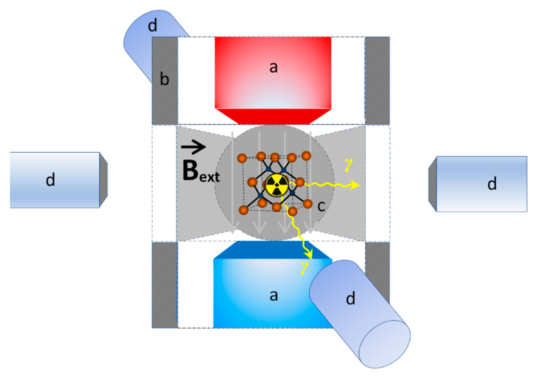
After annealing, the samples were mounted into magnets with strengths of 0.48 T or 2.1 T and were then measured at room temperature and 77 K in liquid nitrogen using the TDPAC spectroscopy. Detailed descriptions of the 0.48 T and the 2.1 T setups have been presented in [24,25,26]. The 2.1 T magnet could not be used for measurements in liquid nitrogen (77 K) because of its large size. It is a cylinder with diameter d = 12 cm and height h = 10 cm, making it impossible to place the whole system (2.1 T magnet and sample) into a small liquid nitrogen dewar. If a larger dewar were used to contain this system, the distance from the sample to each detector would be too great (>6 cm) and the gamma signals would be too weak to be recorded. The magnets containing the samples were placed at the center of a planar configuration of four detectors, with the magnetic field oriented perpendicular to the plane as illustrated in Figure 1.
3. Results and Discussion
3.1. Magnetic Interaction at Room Temperature
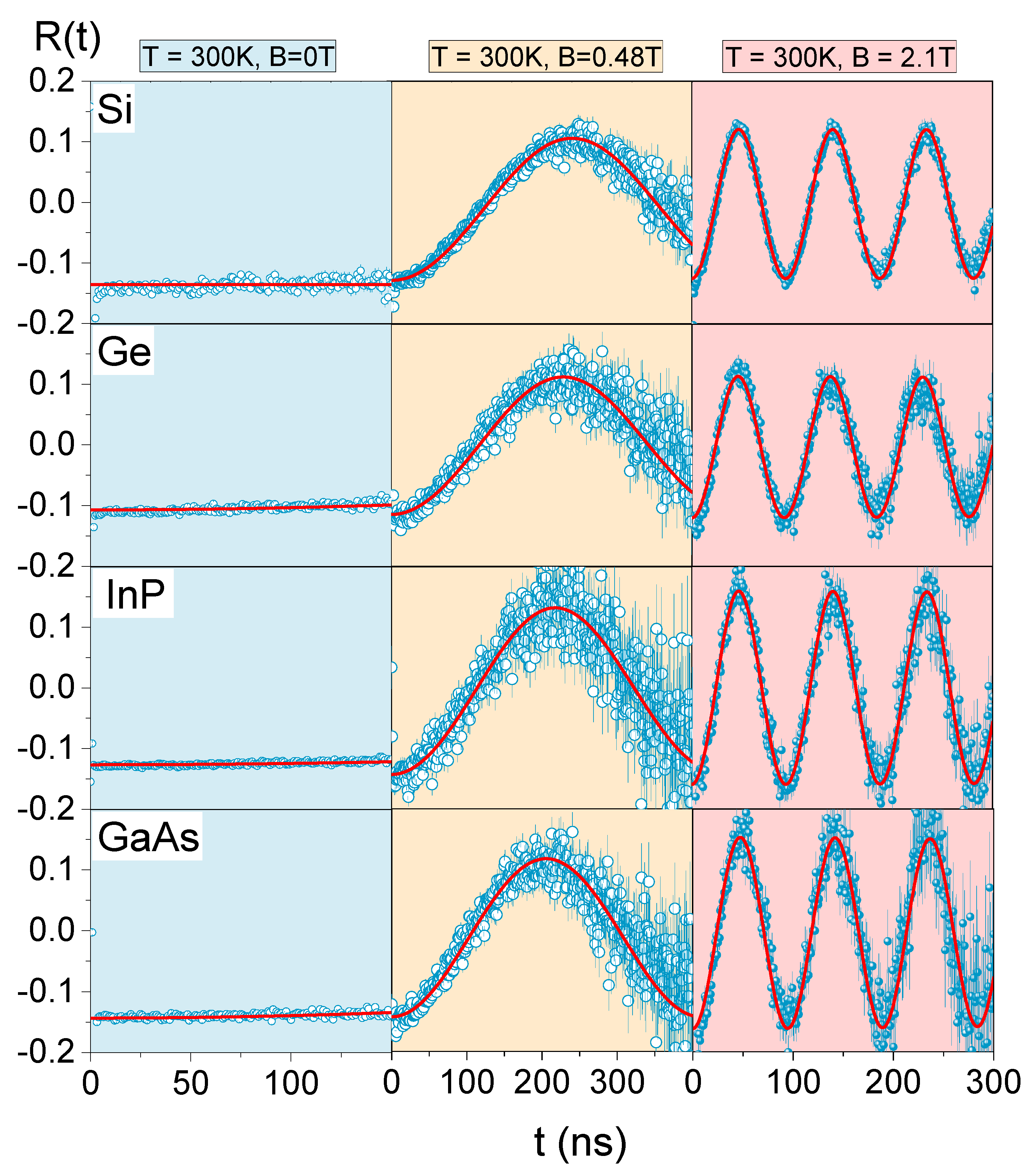
The experimentally measured Larmor frequencies are shown in Table 2 and agree well with the computed values for isolated radioactive atoms (i.e., not implanted in a material). For the intermediate state of spin ( Js), the magnetic moment is µ = −0.7656(25) µN (µN = 5.05 × 10⁻²⁷ J/T: the nuclear magneton) [11]. With magnetic fields of Bz = 0.48 T and 2.1 T, the calculated values of the Larmor frequency using expression (2) are 6.9 Mrad/s and 30.9 Mrad/s, respectively. The agreement between these experimental values and the free space calculated values confirms that no defects are present in the semiconductors in the probe vicinity. The spectra in Figure 2 show a constant precession frequency and constant amplitude, because the magnetic fields have a constant magnitude and direction during the measurement. The distribution of the Larmor frequencies is extremely narrow (). The environments of the probe nuclei thus have cubic symmetry and contain practically no intrinsic point defects in the vicinity of the probe ions. After the annealing treatment, all probe atoms replace the host atoms at lattice sites of cubic symmetry [18,19,20]. The atomic size discrepancy between the In-probe and the lattice atoms (Table 3) might cause a lattice distortion which represents a mechanical dilatation center induced by the probe. Such a dilatation center does not alter the signal at the probe in cubic symmetry. The intrinsic point defect concentration is too low to be itself detected by the TDPAC technique as the probability of finding another defect in the direct vicinity of the probe is very low.
Without a magnetic field, there is no perturbation of the angular correlation (Figure 2). This means that neither electric field gradients are present, nor magnetic fields. This is expected in a cubic crystal, if neither a defect atom nor an electronic defect is associated with the probe ion. Under an external magnetic field, the precession of the nuclei is very well visible. As far as the value of the magnetic moment is known, the precession frequencies correspond to the expected values of open space. Table 2 summarizes the observed frequencies. The slight diamagnetic susceptibility of all four materials does not change the observed precession frequencies in a systematic manner. In particular, under a large external field, the frequencies are all identical within experimental error. For the low applied field, a small difference in the Larmor frequencies can be found between the four semiconductors. The measured Larmor frequencies, around 33 Mrad/s, are similar to the 32(1) Mrad/s in the study by Schell et al. [15]. The 6% difference from the value expected (30.9 Mrad/s) from previous determination of the magnetic moment of the nucleus [11] likely occurs due to the structure of the 2.1 T magnet pot. It consists of two cylindrical permanent magnets housed in a cylinder made of a combination of aluminum, lead, and Armco iron [25]. Positioning the sample at the right field spot is a potential systematic error.
3.2. Electric Quadrupole and Magnetic Dipole Interactions at 77 K
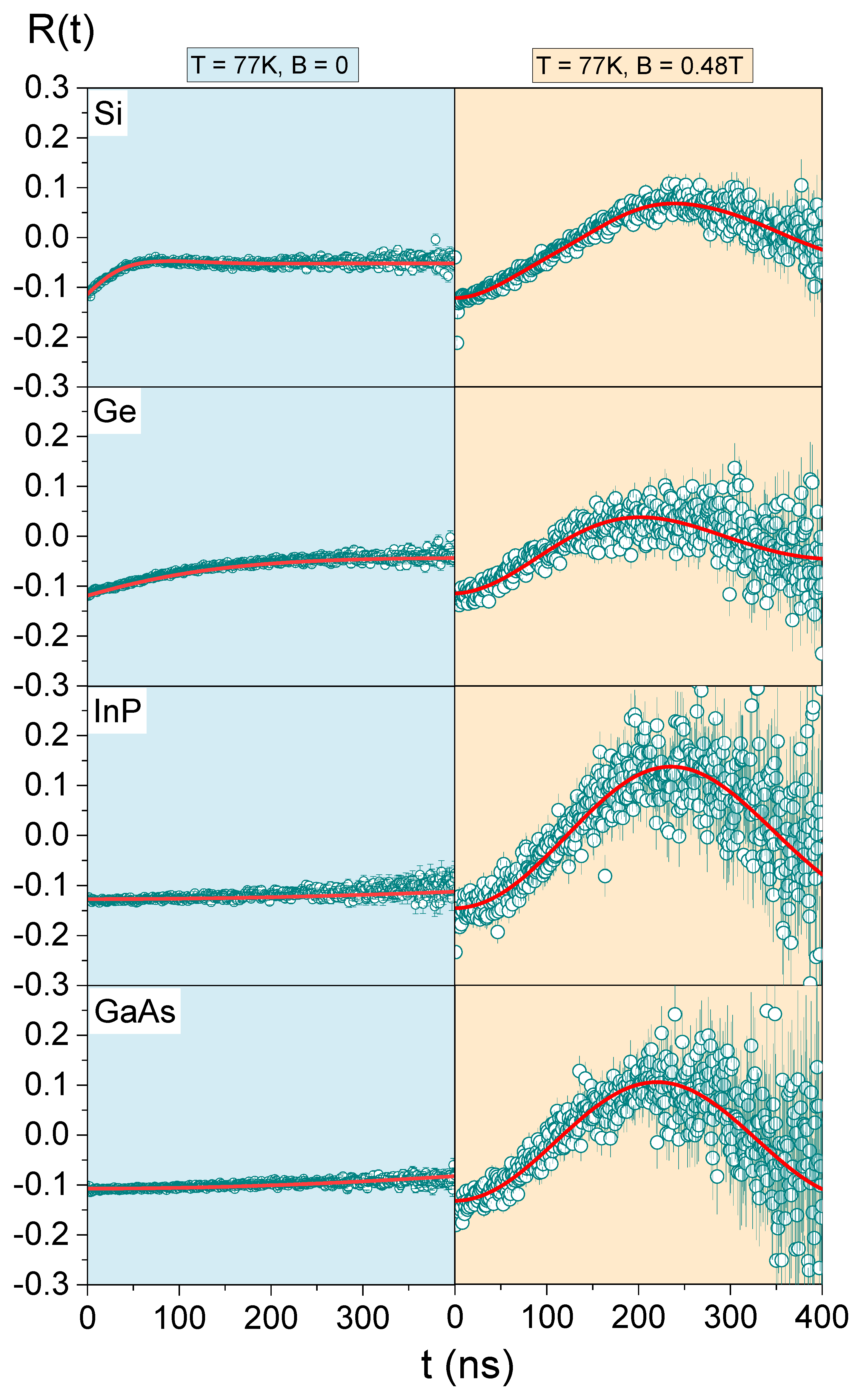
For GaAs and InP, the angular perturbation without a magnetic field remains unperturbed, also at 77 K. So, nothing changes compared to room temperature. For Ge and Si, a perturbation is well visible, prompting questions as to why this occurs. As the measurements were made in the identical crystals, the presence of electric defects/dopants cannot have changed with respect to room temperature. Furthermore, no change in crystal structure arises.
One peculiarity about the isotope 111In must be known to understand the observed spectra. To feed the nuclear decay, it captures an electron from its proper electronic shell in order to transform to 111Cd, which is the nucleus of the actual measurement. Typically, this electronic state (hole) is refilled within the timeframe of atomic shell rearrangement (in the picosecond range). Thus, the atom at the time of measurement (first pixels after 0.5 ns) is already in a static environment. For very low temperatures, however, the electronic cascade may have been incomplete, which is called the after-effect [41]. This means that an outer shell electronic state may survive for a sufficient period of time to perturb the angular correlation at longer times. For this to happen, a non-symmetric electric environment must be generated from this residual hole at the probe. The simplest configuration is a hole state in an adjacent atom or on the bond to an adjacent atom. Indium is present in InP. Cd has practically the same electronic shell as In. Thus, atoms in the direct vicinity of the probe provide electronic states at the same levels as the probe atom itself. The tunneling of the hole away from the probe is thus easy (quantum tunneling in chemical bonds [42]), the spectrum remains unperturbed. GaAs is more complex. Like in InP, In will occupy a Ga-site due to the matching valence. The bond to the adjacent As is covalent, but the covalent bond has a polar character due to the different valences of the alloy atoms. For the nuclear reaction, one such bond electron must be used to refill the inner shell of Cd. The residual electronic state on the bond is a single trap state in the band gap. Its refilling apparently is also sufficiently fast in GaAs as to not perturb the angular correlation.
In silicon and germanium, Cd2+ is potentially a doubly charged defect. Thus, it can be Cd2+, Cd+ or Cd0, for which the latter is equivalent to an unaltered band of the semiconductor. A perturbation in the spectra will be visible, if an alteration of the electronic environment happens past 0.5 ns or up to 400 ns, the latter being the maximum measurement time. Strong changes will arise from 1 ns to 50 ns time constant, for lower frequencies the influence will be small. Thus, in Si as well as Ge, the electronic shell is altered in this time constant range at 77 K. It must be understood that any geometrically symmetric environment will not generate a perturbation of the angular correlation, because the electric field gradient vanishes. Thus, a cubic crystal and a cubic crystal with a symmetric electronic defect state will yield no perturbation. Only if the electronic defect state is located on a chemical bond to the neighboring atoms is the symmetry broken and a perturbation of the angular correlation arises. The results of this section are thus that a hole localized on a bond to an adjacent Si (Ge) atom is populated or depopulated in megahertz up to the 1 GHz range. This defect constitutes the electric field gradient.
Referring to Table 2, a correlation between the occurrence of the after-effect with electron mobility seems to be present, while it seems unrelated to hole mobility. The picture becomes more complex if one considers the mobility data at 77 K. At this temperature, there is no correlation between electron or hole mobilities (Table 4) with the occurrence of the after-effect. Particularly, there is no direct influence of intrinsic carrier concentration of the hosts on the after-affect because the number of intrinsic carrier concentrations of the samples at 77 K (Table 4) are extremely low compared to those at 300 K (Table 2). Thus, the fact that Cd represents a doubly charged defect in Si as well as Ge retards the refilling of the electronic shell into the few nanoseconds range and generates the after-effect. In the compound semiconductors InP and GaAs, Cd is a singly charged defect. The tunneling away of the residual hole or refilling with free carriers from the band states is sufficiently fast. Considering the very low level of intrinsic carrier density at this temperature, an enhanced tunneling probability is the most likely process to remove the electron from the Cd-defect.
For measurements under the magnetic field, the samples were mounted into the 0.48 T magnet as shown in Figure 1 and then placed in liquid nitrogen (77 K). The PAC spectra and fits of the annealed samples are presented in Figure 3. The Larmor frequencies (ωL) and dynamic quadrupole frequencies (ω0) are given in Table 4. They are practically identical with those at room temperature. Thus, no additional effect on the magnetic interaction is observed. The crystal yields the same numbers. For GaAs and InP, no dynamic electric interaction is observed for all measurement temperatures (ω0 ≈ 0) [7] and, therefore, only the magnetic interaction is considered. For Si, a small contribution of a quadrupole frequency is measured at 77 K under the application of the external magnetic field: ω0(Si) ≈ 4 Mrad/s. No quadrupole interaction is found for Ge: ω0(Ge) = 0 Mrad/s (without an external magnetic field: ω0(Si) ≈ 15 Mrad/s and ω0(Ge) ≈ 3 Mrad/s). The corresponding R(t) spectra are shown in Figure 3 (beige layer). The dynamic interaction does not contribute to the spectra significantly under the magnetic field. As we can only access a finite time in this type of measurement, the effect of electronic re-arrangement may be hidden in the statistical background at long measurement times.
4. Conclusions
The TDPAC technique was used in four classical cubic semiconductors. As expected for the symmetry of the crystal, no electric field gradients are observed. This also means that no adjacent defects are localized close to the substitutional probe ion In. The externally applied magnetic fields generate Larmor frequencies practically identical to open space. No influence of the semiconductor itself is seen for the magnetic interaction.
The interesting effects arise at low temperature (77 K) when electronic charge carriers become scarce. InP and GaAs still show electrically unperturbed spectra and the effect of an unaltered magnetic interaction. In contrast, silicon and germanium exhibit the after-effect. In these two semiconductors, the Cd probe is a doubly charged defect. Its electric reconstruction after electron capture takes a longer time than in the other two semiconductors. We explain this difference by two factors: First, the compound semiconductors have to only provide a single electron, because In substitutes a trivalent lattice site (either In itself or Ga) and Cd then only forms a single electronic trap state. In silicon and germanium, the after-effect is visible, which means that refilling of the electronic states is retarded. This also means that not only is one electron missing after the electron capture in Si and Ge, but via Auger-like effects, Cd is initially doubly charged with respect to the lattice. The refilling of these two states takes a longer time than to only refill one empty state, despite the much higher electron and hole mobilities at low temperatures.
A second effect can be related to an enhanced tunneling probability from Cd to the adjacent In-atoms in InP. As the electronic shells are practically identical, any vacant intermediate electronic state can be refilled from adjacent In-atoms as the same electronic states prevail.
Under the magnetic field, the differences become negligible. All four semiconductors show the Larmor frequency, and only in germanium is a small contribution by electronic restructuring found in the fits. It can be interpreted as stemming from the same process as in the field free case.
Author Contributions
T.T.D. did all measurements, fits, and wrote the manuscript. D.C.L. and J.S. contributed to the writing of the manuscript, data analysis and data interpretation. R.B. and C.N. were responsible for 111In probe implantations. All authors have read and agreed to the published version of the manuscript.
Funding
This work was supported by the Federal Ministry of Education and Research, BMBF, through grant 05K16PGA, and the German Academic Exchange Service, DAAD, in collaboration with Conselho Nacional de Desenvolvimento Científico e Tecnológico, CNPq, through grant no. 290102/2011-1.
Institutional Review Board Statement
Not applicable.
Informed Consent Statement
Not applicable.
Data Availability Statement
Not applicable.
Acknowledgments
We thank P.D. Vianden and all members of the TDPAC research group in HISKP, University of Bonn, who were always available to provide help when needed.
Conflicts of Interest
The authors declare no conflict of interest.
References
- Gupta, S.; Navaraj, W.T.; Lorenzelli, L.; Dahiya, R. Ultra-thin Chips for High-performance Flexible Electronics. Npj Flex. Electron. 2018, 2, 1–17. [Google Scholar] [CrossRef]
- Sigillito, A.J.; Jock, R.M.; Tyryshkin, A.M.; Beeman, J.W.; Haller, E.E.; Itoh, K.M.; Lyon, S.A. Electron Spin Coherence of Shallow Donors in Natural and Isotopically Enriched Germanium. Phys. Rev. Lett. 2015, 115, 247601. [Google Scholar] [CrossRef] [PubMed] [Green Version]
- Moss, S.J.; Ledwith, A. The Chemistry of the Semiconductor Industry, 1st ed.; Springer Science and Business Media: Dordrecht, The Netherlands, 1989; ISBN 978-0-216-92005-7. [Google Scholar]
- Vinod, K.K. Extreme-Temperature and Harsh-Environment Electronics, Chapter 3 Temperature Effects on Semiconductors; IOP Publishing Ltd.: Bristol, UK, 2017. [Google Scholar] [CrossRef]
- Barber, H.D. Effective Mass and Intrinsic Concentration in Silicon; Solid-State Electronics, Pergamon Press: Great Britain, UK, 1967; Volume 10, pp. 1039–1051. [Google Scholar]
- Ingo, T.-S.; Manfred, R.; Matthias, S.; Ronny, S.; Thomas, F.; Thomas, O. Carrier Mobility in Semiconductors at Very Low Temperatures. Eng. Proceeding 2021, 6, 86. [Google Scholar]
- Dang, T.T.; Schell, J.; Lupascu, D.C.; Vianden, R. Dynamic Quadrupole Interactions in Semiconductors. J. Appl. Phys. 2018, 123, 165109. [Google Scholar] [CrossRef]
- Uemura, Y. Landau Levels and Electronic Properties of Semiconductor Interface. Jpn. J. Appl. Phys. 1974, 13, 17–24. [Google Scholar] [CrossRef]
- Watkins, G.D. Chapter 1–EPR and ENDOR Studies of Defects in Semiconductors. Semicond. Semimet. 1998, 51A, 1–43. [Google Scholar]
- Cordeiro, M.R.; Carbonari, A.W.; Saxena, R.N. Study of Defects in Silicon by Means of Perturbed Angular Gamma-Gamma Correlation Spectroscopy. In Proceedings of the International Nuclear Atlantic Conference–INAC 2005 Santos, Santos, Brazil, 28 August–2 September 2005; Associação Brasileira De Energia Nuclear–Aben: Rio de Janeiro, Brazil, 2005. ISBN 85-99141-01-5. [Google Scholar]
- Schatz, G.; Weidinger, A. Nuclear Condensed Matter Physics; Wiley: Chichester, UK, 1996; ISBN 0-471-95479-9. [Google Scholar]
- Abragam, A.; Pound, R.V. Influence of Electric and Magnetic Fields on Angular Correlations. Phys. Rev. 1953, 92, 943–962. [Google Scholar] [CrossRef]
- Wolf, H.; Guan, Z.; Natter, H.; Hempelmann, R.; Wichert, T. Investigation of Grain Growth and Stabilisation of Nanocrystalline Ni. J. Metastable Nanocrystalline Mater. 2001, 10, 247–252. [Google Scholar] [CrossRef]
- Rogers, J.D.; Vasquez, A. Data Reduction in Perturbed Angular Correlation Experiments. Nucl. Instrum. Methods 1975, 130, 539–541. [Google Scholar] [CrossRef]
- Schell, J.; Dang, T.T.; Zyabkin, D.V.; Mansano, R.; Gaertner, D.; Carbonari, A.W. Investigation of the Local Environment of SnO2 in an Applied Magnetic Field. Phys. B Condens. Matter 2020, 586, 412120. [Google Scholar] [CrossRef]
- Freitag, K. A Facility for Ion Implantation in Samples Colder Than 0.5 k. Radiat. Eff. 1979, 44, 185–190. [Google Scholar] [CrossRef]
- Schell, J.; Lupascu, D.C.; Carbonari, A.W.; Mansano, R.D.; Ribeiro, I.S., Jr.; Dang, T.T.; Anusca, I.; Trivedi, H.; Johnston, K.; Vianden, R. Ion Implantation in Titanium Dioxide Thin Films Studied by Perturbed Angular Correlations. J. Appl. Phys. 2017, 121, 145302. [Google Scholar] [CrossRef]
- Pasquevich, A.F.; Vianden, R. Temperature Dependence of the Hyperfine Interactions of 111Cd in Silicon. Phys. Rev. B 1987, 35, 1560–1565. [Google Scholar] [CrossRef] [PubMed]
- Pasquevich, A.F.; Vianden, R. Temperature Dependence of the Hyperfine Interactions of 111Cd in Germanium. Phys. Rev. B 1988, 37, 10858–10861. [Google Scholar] [CrossRef] [PubMed]
- Pasquevich, A.F.; Vianden, R. Time Differential Perturbed Angular Correlation Study of 111In–111Cd in III-V Compounds. Phys. Rev. B 1990, 41, 10956–10962. [Google Scholar] [CrossRef]
- Mola, G.T. Indium-Impurity Pairs in Semiconductors and the Study of the Influence of Uniaxial Stress on Defect Complexes in Silicon. Ph.D. Thesis, HISKP University of Bonn, Bonn, Germany, 6 February 2003; pp. 46–47. Available online: https://tdpac.hiskp.uni-bonn.de/doktorarbeiten/Doktorarbeit-Genene-Tessema-Mola-2003-en.pdf (accessed on 25 January 2022).
- Risse, M. Das Verhalten von Brom in InAs und GaAs, Untersucht mit den Sonden 77Br(77Se), 79Br und 82Br. Ph.D. Thesis, HISKP University of Bonn, Bonn, Germany, 21 June 2000; p. 37. Available online: https://tdpac.hiskp.uni-bonn.de/doktorarbeiten/Doktorarbeit-Monika-Risse-2000.pdf (accessed on 25 January 2022).
- Schneider, F.; Unterricker, S. Radiation Damage and its Annealing Behaviour in InP after Recoil Implantation of 118Sb and 111In Observed by TDPAC. Phys. Status Solidi A 1984, 85, 455–461. [Google Scholar] [CrossRef]
- Müller, K. Hyperfinewechselwirkungen von 100Pd in Ru, RuO2 and RuGa3. Master’s Thesis, Rheinischen Friedrich–Wilhelms–Universität Bonn, Bonn, Germany, 30 December 2009; pp. 15–16. Available online: https://tdpac.hiskp.uni-bonn.de/diplomarbeiten/Diplomarbeit-Krystyna-Mueller-2009.pdf (accessed on 25 January 2022).
- Agarwal, I. Influence of Magnetic Fields on a Defect-Complex in Group-III Nitride Semiconductors. Master’s Thesis, Bonn University, Bonn, Germany, 1 October 2012; pp. 23–24. Available online: https://tdpac.hiskp.uni-bonn.de/diplomarbeiten/Masterarbeit-Ishita-Agarwal-2012.pdf (accessed on 25 January 2022).
- Alfter, I.; Bodenstedt, E.; Hamer, B.; Knichel, W.; Meler, R.; Sajok, R.; Schaefer, T.; Schth, J.; Vianden, R. Core Vibration of 99Tc. Z. Für Phys. A Hadron. Nucl. 1993, 347, 1–14. [Google Scholar] [CrossRef]
- Hudgens, S.; Kastner, M.; Fritzsche, H. Diamagnetic Susceptibility of Tetrahedral Semiconductors. Phys. Rev. Lett. 1974, 33, 1552–1555. [Google Scholar] [CrossRef]
- Wasserrab, T. Die Temperaturabhangigkeit der elektronischen Kenngrofien des eigenleitenden Siliciums. Z. Für Nat. A 1977, 32, 746–749. [Google Scholar] [CrossRef]
- Prince, M.B. Drift Mobilities in Semiconductors. II. Silicon. Phys. Rev. 1954, 93, 1204. [Google Scholar] [CrossRef]
- Jacoboni, C.; Canali, C.; Ottaviani, G.; Alberigi Quaranta, A. A review of some charge transport properties of silicon. Solid-State Electron. 1977, 20, 77–89. [Google Scholar] [CrossRef]
- Morin, F.J.; Maita, J.P. Electrical Properties of Silicon Containing Arsenic and Boron. Phys. Rev. 1954, 94, 1525. [Google Scholar] [CrossRef]
- Prince, M.B. Drift Mobilities in Semiconductors. I. Germanium. Phys. Rev. 1953, 92, 681–687. [Google Scholar] [CrossRef]
- Busch, G.; Kern, R. Die magnetischen Eigenschaften der A-III B-V-Verbindungen. Helv. Phys. Acta 1959, 32, 29. [Google Scholar]
- Betko, J.; Merinsky, K. On the temperature dependence of the intrinsic concentration in semi-insulating InP determined from galvanomagnetic measurements. Phys. Status Solidi A 1993, 135, K67. [Google Scholar] [CrossRef]
- Zhu, L.D.; Chan, K.T.; Ballantyne, J.M. Very high mobility InP grown by low pressure metalorganic vapor phase epitaxy using solid trimethylindium source. Appl. Phys. Lett. 1985, 47, 47–48. [Google Scholar] [CrossRef]
- Weisbuch, C.; Hermann, C. Optical detection of conduction electron spin resonance in InP. Solid State Commun. 1975, 16, 659–661. [Google Scholar] [CrossRef]
- Blakemore, J.S. Intrinsic density ni (T) in GaAs: Deduced from band gap and effective mass parameters and derived independently from Cr acceptor capture and emission coefficients. J. Appl. Phys. 1982, 53, 520. [Google Scholar] [CrossRef]
- Lancefield, D. Properties of Gallium Arsenide; Brozel, M.R., Stillman, G.E., Eds.; INSPEC/IEE: London, UK, 1996; pp. 46–53. [Google Scholar]
- Wiley, J.D. Semiconductor and SemimetalsWillardson, R.K., Beer, A.C., Eds.; Chapter 2 Mobility of Holes in III-V CompoundsWillardson, R.K., Beer, A.C., Eds.; Academic Press: New York, NY, USA, 1975; Volume 10, p. 91.
- Slater, J.C. Atomic Radii in Crystals. J. Chem. Phys. 1964, 41, 3199–3204. [Google Scholar] [CrossRef]
- Lupascu, D.; Habenicht, S.; Lieb, K.P.; Neubauer, M.; Uhrmacher, M.; Wenzel, T. Relaxation of Electronic Defects in Pure and Doped La2O3 Observed by Perturbed Angular Correlations. Phys. Rev. B 1996, 54, 871–883. [Google Scholar] [CrossRef]
- Hermann, H.; Hans, C.W. The Physics of Atoms and Quanta: Introduction to Experiments and Theory; Springer: Berlin/Heidelberg, Germany, 2005. [Google Scholar]
- Misiakos, K.; Tsamakis, D. Accurate measurements of the silicon intrinsic carrier density from 78 to 340 K. J. Appl. Phys. 1993, 74, 3293–3297. [Google Scholar] [CrossRef]
- Canali, C.; Jacoboni, C.; Nava, F.; Ottaviani, G.; Quaranta, A.A. Electron drift velocity in silicon. Phys. Rev. B 1975, 12, 2265–2284. [Google Scholar] [CrossRef]
- Ottaviani, G.; Reggiani, L.; Canali, C.; Nava, F.; Quaranta, A.A. Hole drift velocity in silicon. Phys. Rev. B 1975, 12, 3318–3329. [Google Scholar] [CrossRef]
- Jacoboni, C.; Nava, F.; Canali, C.; Ottaviani, G. Electron drift velocity and diffusivity in germanium. Phys. Rev. B 1981, 24, 1014–1026. [Google Scholar] [CrossRef] [Green Version]
- Ottaviani, G.; Canali, C.; Nava, F.; Mayer, J.W. Hole drift velocity in high-purity Ge between 8 and 220 K. J. Appl. Phys. 1973, 44, 2917–2918. [Google Scholar] [CrossRef]
- Rode, D.L. Semiconductors and SemimetalsWillardson, R.K., Beer, A.C., Eds.; Chapter 1 Low-Field Electron TransportWillardson, R.K., Beer, A.C., Eds.; Academic Press: New York, NY, USA, 1975; Volume 10.
- Madelung, O.; Rössler, U.; Schulz, M. Gallium Arsenide (GaAs), Intrinsic Carrier Concentration, Electrical and Thermal Conductivity. Group IV Elements, IV-IV and III-V Compounds. Part b-Electronic, Transport, Optical and Other Properties. In Landolt-Börnstein-Group III Condensed Matter; Springer: Berlin/Heidelberg, 2002; Volume 41A1β, pp. 1–8. ISBN 978-3-540-42876-3. [Google Scholar] [CrossRef]
- Look, D.C. Properties of Gallium Arsenide; INSPEC/IEE: London, UK, 1990. [Google Scholar]
Figure 1.
Schematic diagram of the magnetic field setup (0.48 T): Semiconductors doped with a radioactive isotope were placed in a uniform magnetic field, where (a) represents the permanent magnets, (b) is an iron casing to shield the magnetic field, (c) is the position of the sample, and (d) are the detectors.

Figure 2.
The fitted PAC spectra of the annealed samples in magnetic fields of 0 T (reproduced from Figure 3 in Ref. [7]), 0.48 T and 2.1 T at room temperature.

Figure 3.
The PAC spectra measured at 77 K with 0 T (blue layer) and 0.48 T (beige layer) magnetic fields.
Figure 3.
The PAC spectra measured at 77 K with 0 T (blue layer) and 0.48 T (beige layer) magnetic fields.


Table 1.
Detailed parameters of implantation [7].
Table 1.
Detailed parameters of implantation [7].
| Implantation Energy (keV) | Incident Angle (o) | Fluence/Dose (ions/cm2) | Implantation Depth (nm) | |
|---|---|---|---|---|
| Si | 90 | 10 | 8.1 × 10¹² | 12 |
| Ge | 160 | 10 | 3.8 × 10¹² | 30 |
| GaAs | 160 | 10 | 6.3 × 10¹² | 30 |
| InP | 160 | 10 | 1.5 × 10¹² | 30 |
Table 2.
Experimental Larmor frequencies L, volume magnetic susceptibility χv, intrinsic carrier concentration ni, electron µe and hole µh mobilities at 300 K.
Table 2.
Experimental Larmor frequencies L, volume magnetic susceptibility χv, intrinsic carrier concentration ni, electron µe and hole µh mobilities at 300 K.
| Sample | [Marad/s] | χv(*) | ni (cm−3) | µe | µh | |
|---|---|---|---|---|---|---|
| 0.48 T | 2.1 T | [cm2/Vs] | [cm2/Vs] | |||
| Si | 6.62(2) | 33.55(2) | −0.531 × 10⁻⁶ [27] | 1.02 × 10¹⁰ [28] | 1500 [29] | 450 [30] |
| Ge | 8.04(1) | 34.35(4) | −1.150 × 10⁻⁶ [27] | 2.33 × 10¹³ [31] | 3900 [32] | 1900 [32] |
| InP | 6.63(1) | 33.48(4) | −1.504 × 10⁻⁶ [33] | 3.3 × 10⁷ [34] | 5400 [35] | 150 [36] |
| GaAs | 7.18(2) | 33.23(7) | −1.225 × 10⁻⁶ [27] | 2.1 × 10⁶ [37] | 8865 [38] | 400 [39] |
(*) These values are expressed as volume magnetic susceptibility by the relation where is density near room temperature (g/cm3), M is molar mass (g/mol), is molar magnetic susceptibility (cm3/mol).
Table 3.
Atomic (covalent) radii in Ångstroms [40].
Table 3.
Atomic (covalent) radii in Ångstroms [40].
| Ge | Si | In | P | Ga | As | Cd | |
|---|---|---|---|---|---|---|---|
| Atomic radius [Å] | 1.25 | 1.10 | 1.55 | 1.00 | 1.30 | 1.15 | 1.55 |
Table 4.
The experimental Larmor, quadrupole frequencies without external magnetic field (B = 0) and with B = 0.48 T, intrinsic carrier concentration ni, and electron µe and hole µh mobilities at 77 K.
Table 4.
The experimental Larmor, quadrupole frequencies without external magnetic field (B = 0) and with B = 0.48 T, intrinsic carrier concentration ni, and electron µe and hole µh mobilities at 77 K.
| Samples | T = 77 K, B = 0 | T = 77 K, B = 0.48 T | ni [cm−3] | µe [cm2/Vs] | µh [cm2/Vs] | |
|---|---|---|---|---|---|---|
| [Marad/s] | [Marad/s] | [Marad/s] | ||||
| Si | 14.88(9) | 3.99(3) | 6.49(1) | 1.9 × 10⁻²⁰ [43] | 10,000 [44] | 10,000 [45] |
| Ge | 2.89(2) | 0 | 8.25(1) | - | 20,000 [46] | 400,000 [47] |
| InP | 0.64(1) | 0 | 6.45(2) | - | 300,000 [48] | 14,800 [36] |
| GaAs | 0.84(1) | 0 | 7.12(2) | 2.3 × 10⁻³⁴ [49] | 200,000 [38] | 10,272 [50] |
Publisher’s Note: MDPI stays neutral with regard to jurisdictional claims in published maps and institutional affiliations. |
© 2022 by the authors. Licensee MDPI, Basel, Switzerland. This article is an open access article distributed under the terms and conditions of the Creative Commons Attribution (CC BY) license (https://creativecommons.org/licenses/by/4.0/).
Share and Cite
MDPI and ACS Style
Dang, T.T.; Schell, J.; Beck, R.; Noll, C.; Lupascu, D.C. The Local Exploration of Magnetic Field Effects in Semiconductors. Crystals 2022, 12, 560. https://0-doi-org.brum.beds.ac.uk/10.3390/cryst12040560
AMA Style
Dang TT, Schell J, Beck R, Noll C, Lupascu DC. The Local Exploration of Magnetic Field Effects in Semiconductors. Crystals. 2022; 12(4):560. https://0-doi-org.brum.beds.ac.uk/10.3390/cryst12040560
Chicago/Turabian StyleDang, Thien Thanh, Juliana Schell, Reinhard Beck, Cornelia Noll, and Doru C. Lupascu. 2022. "The Local Exploration of Magnetic Field Effects in Semiconductors" Crystals 12, no. 4: 560. https://0-doi-org.brum.beds.ac.uk/10.3390/cryst12040560
Note that from the first issue of 2016, this journal uses article numbers instead of page numbers. See further details here.