
In Silico Investigation of the Impact of Hole-Transport Layers on the Performance of CH3NH3SnI3 Perovskite Photovoltaic Cells

Abstract
:1. Introduction
- high carrier mobility to increase the fill factor (FF);
- a wide optical band gap and high transparency to minimize optical losses;
- high resistance to water, light and heat;
- low cost of materials and production;
- environmental friendliness.
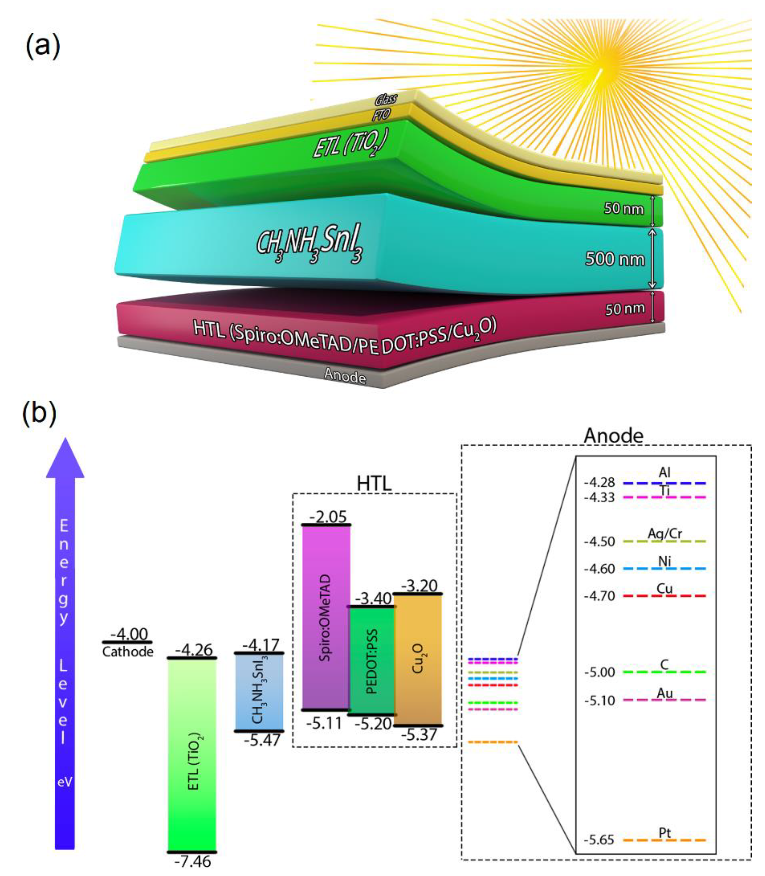
2. Method
- –
- Structure 1. TiO2/CH3NH3SnI3/Spiro-OMeTAD;
- –
- Structure 2. TiO2/CH3NH3SnI3/PEDOT:PSS;
- –
- Structure 3. TiO2/CH3NH3SnI3/Cu2O.
3. Results
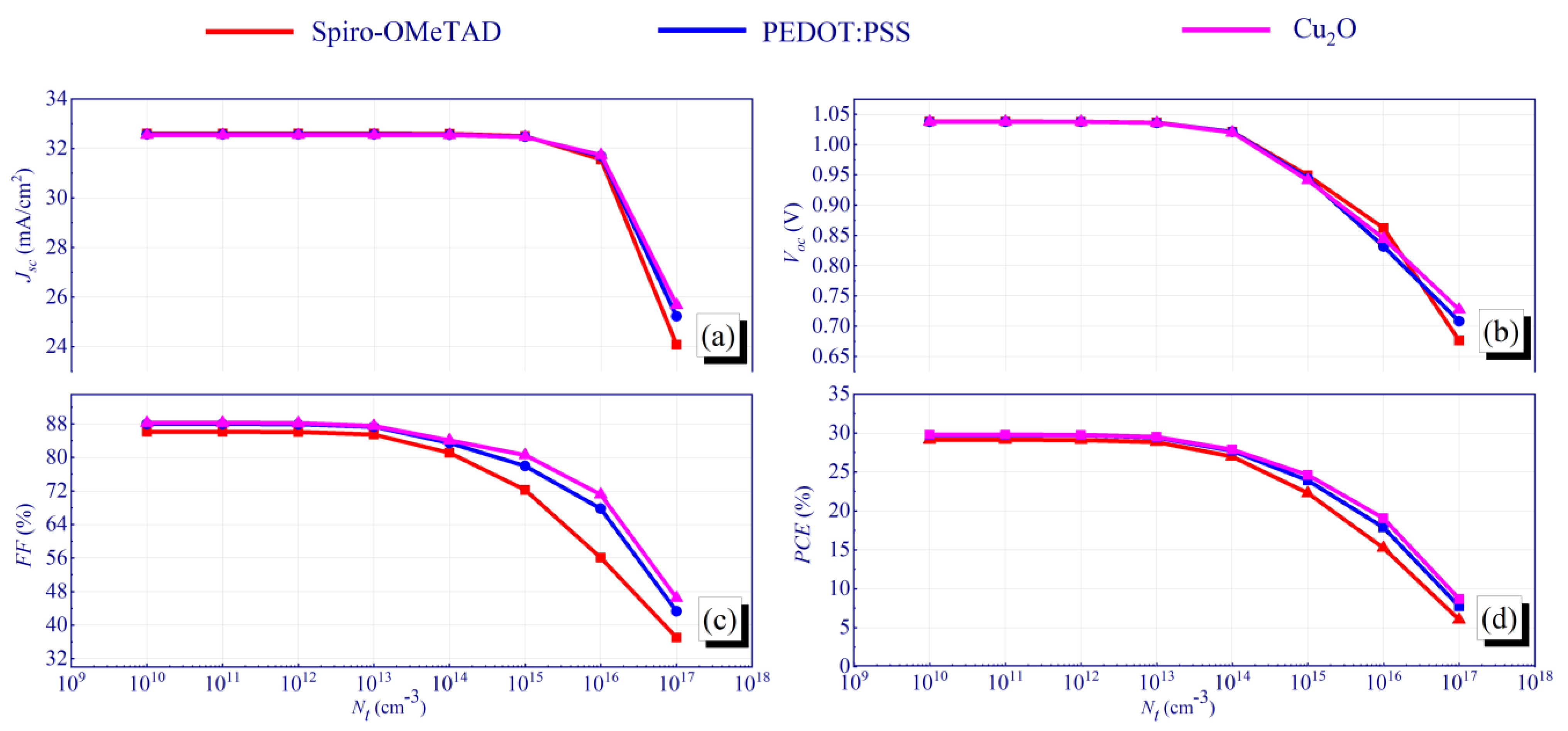
3.1. Influence of Bulk Defect Density on JSC, VOC, FF, PCE in the Absorber Layer
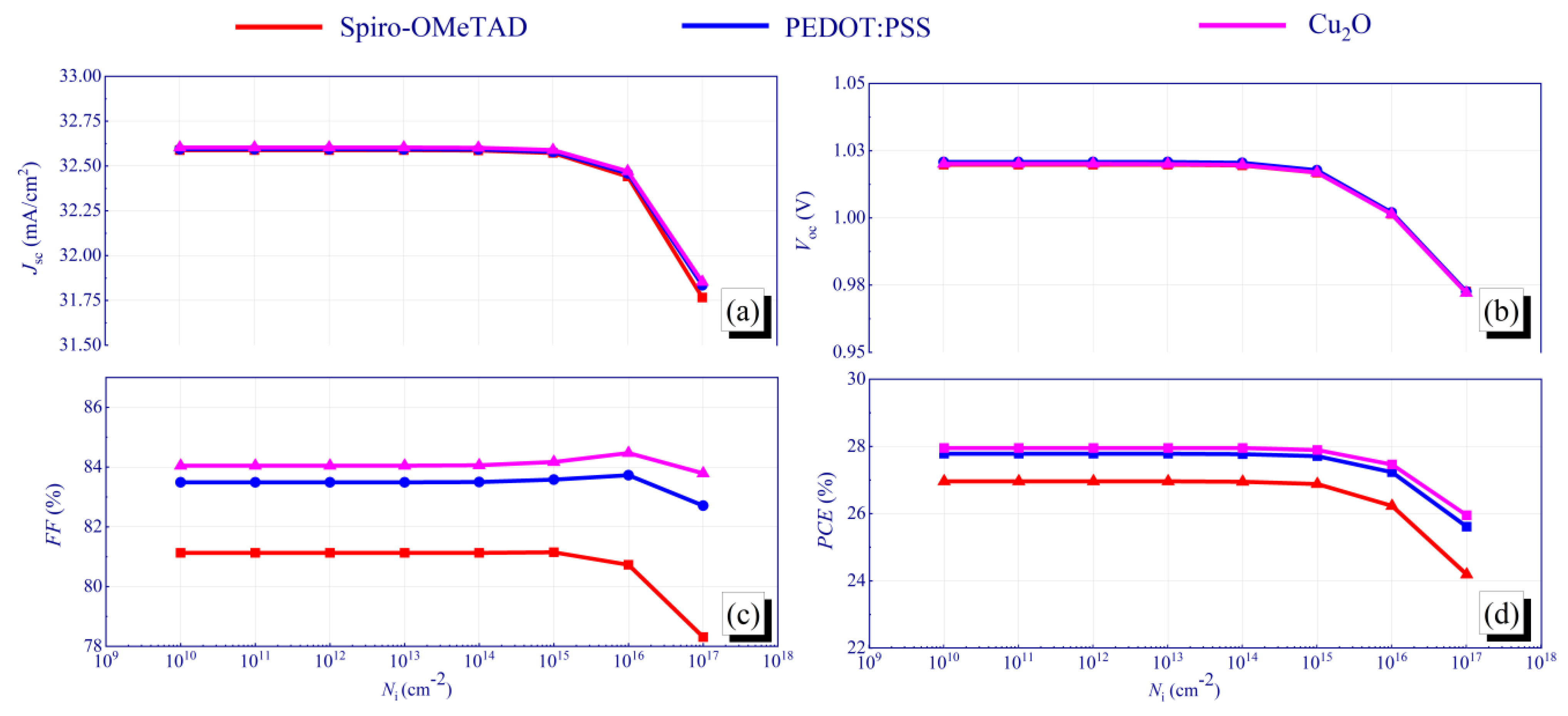
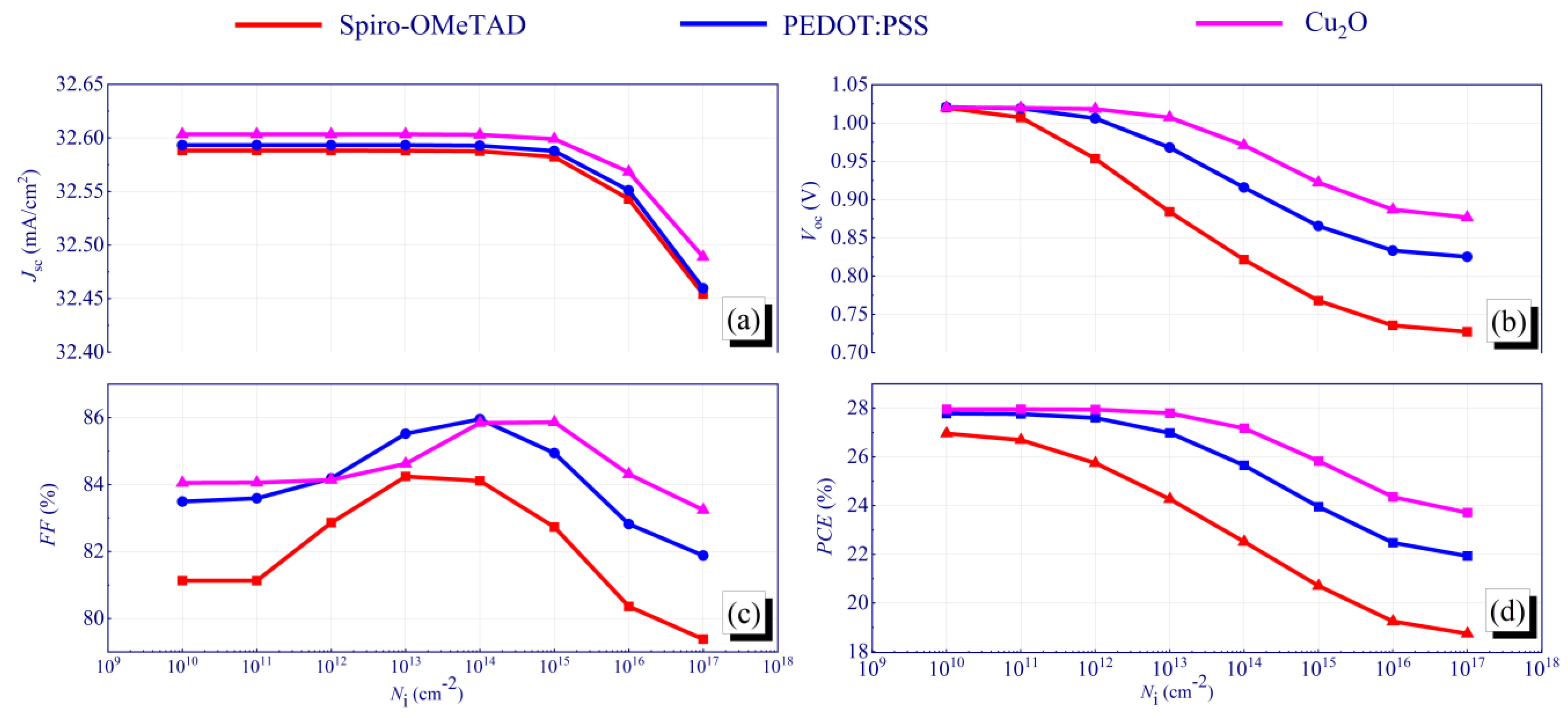
3.2. Influence of the Density on JSC, VOC, FF, PCE of Interfacial Defects
3.3. Influence of the Metal Contact on the Device Performance
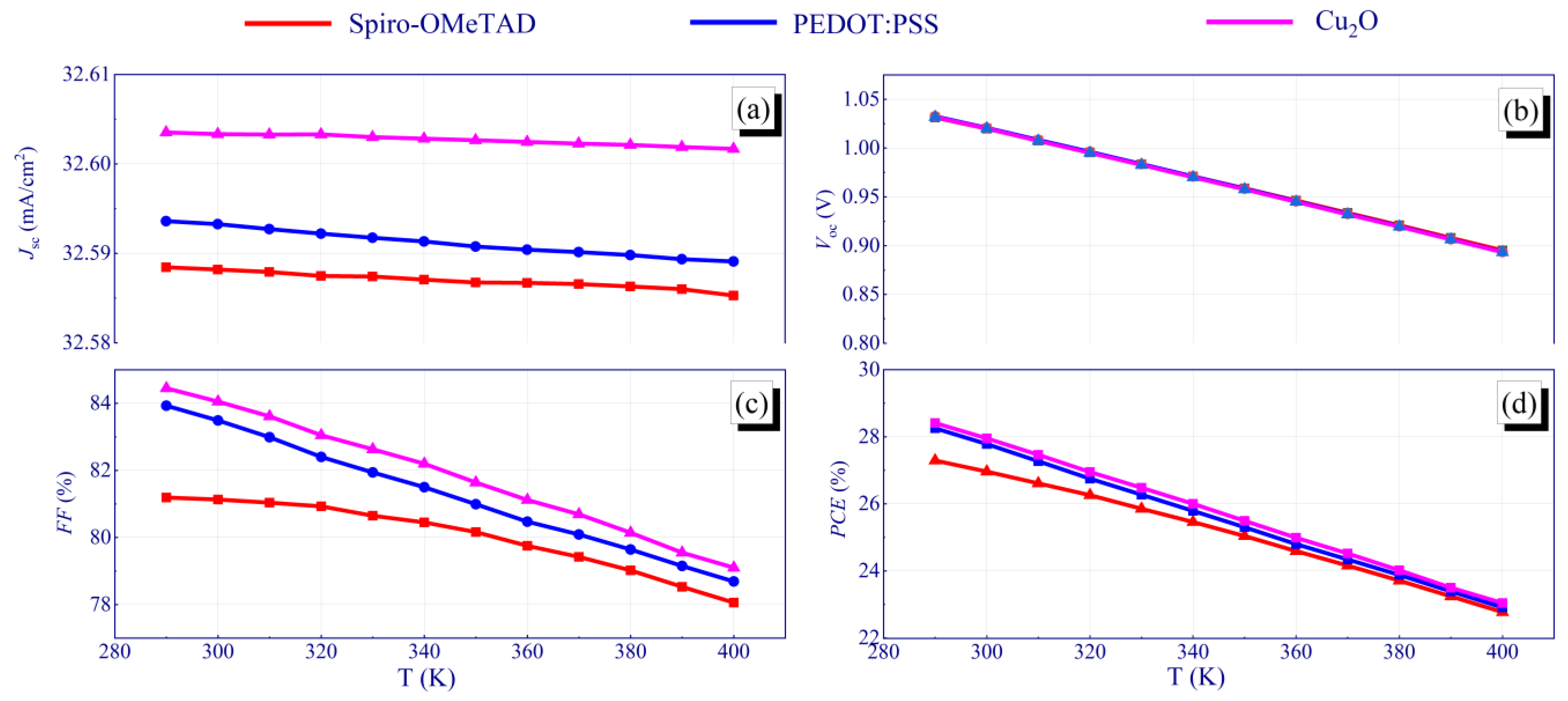
3.4. Influence of Temperature on the Device Performance
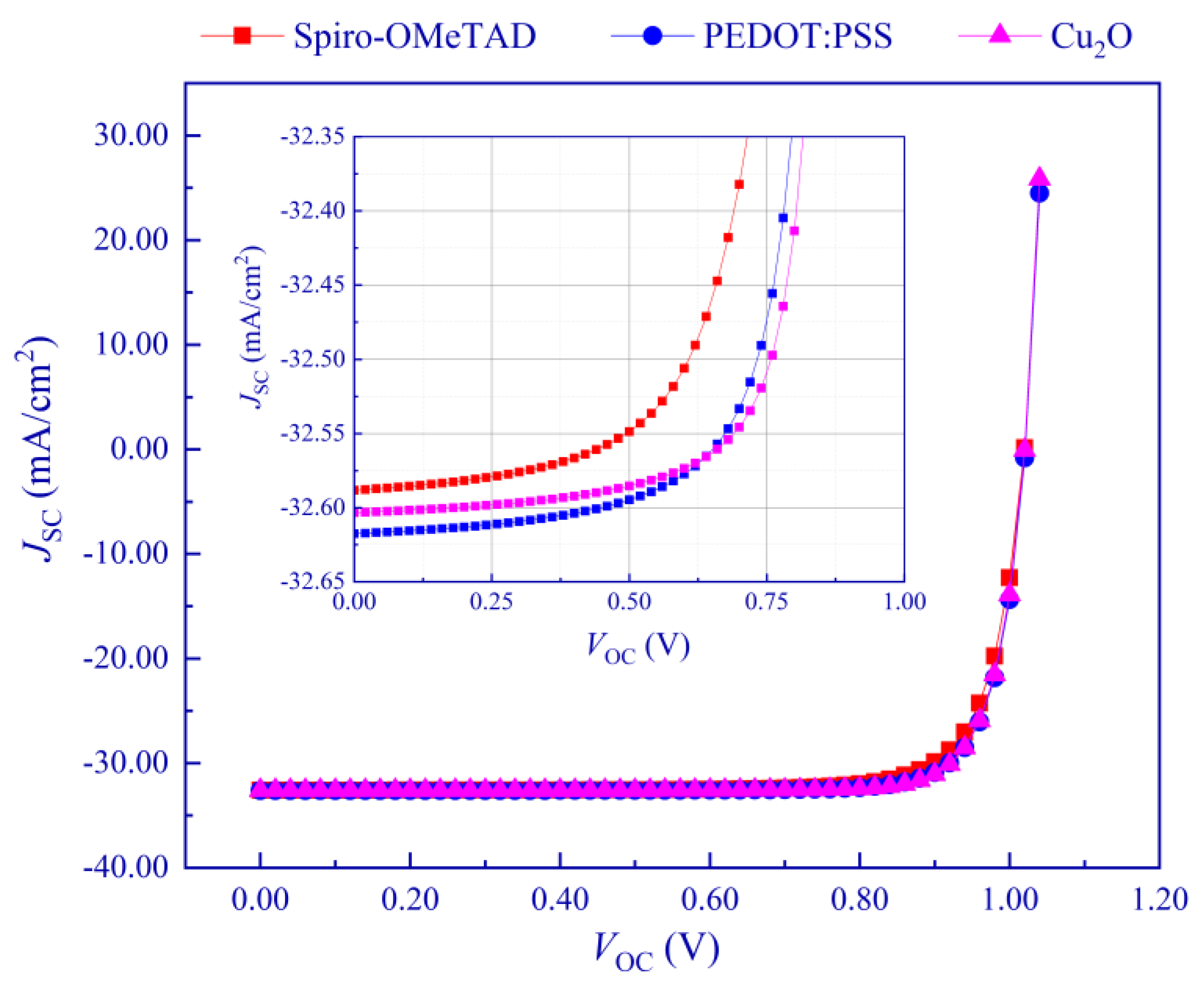
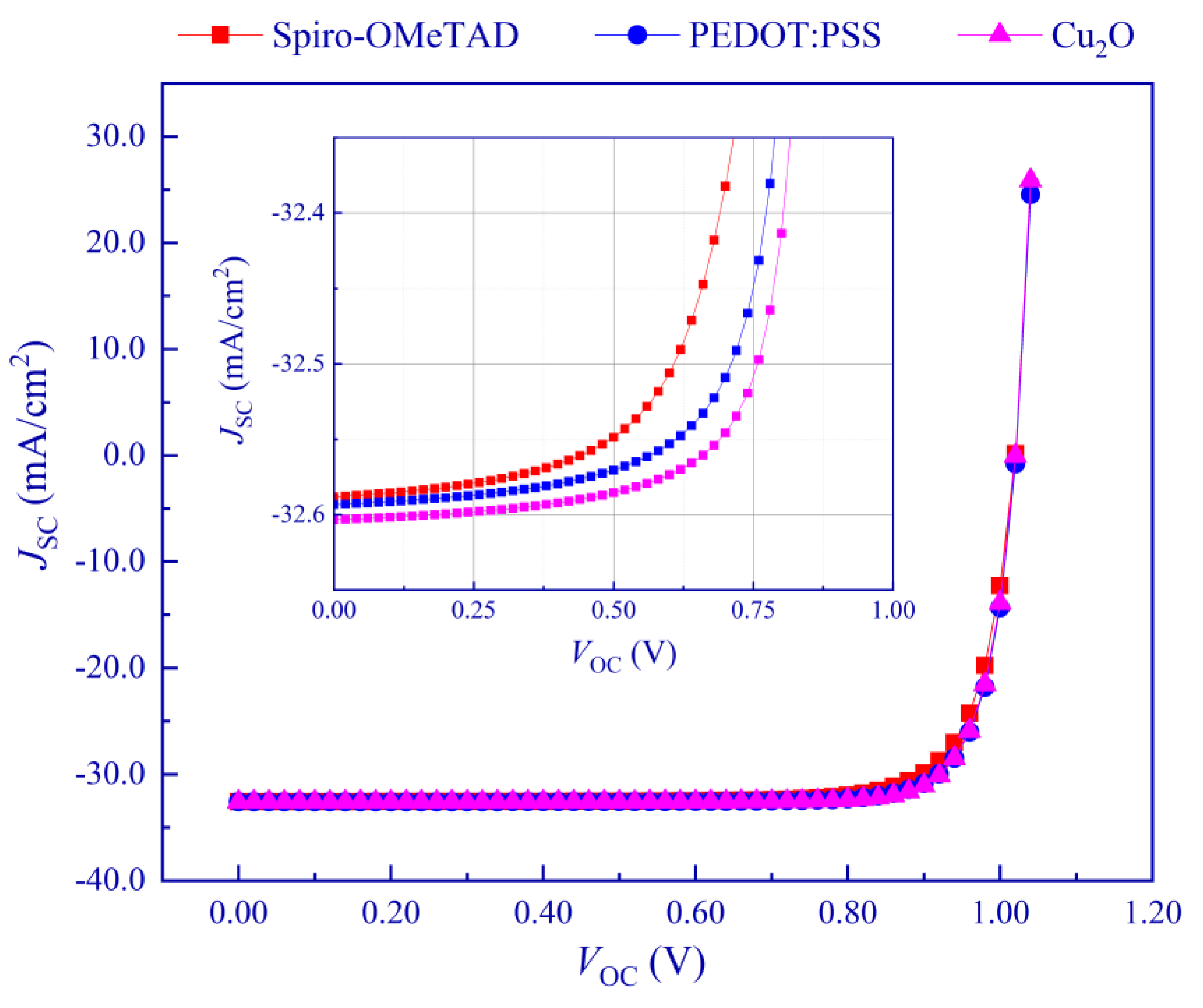
3.5. Comparison of J-V Characteristics for Different HTLs
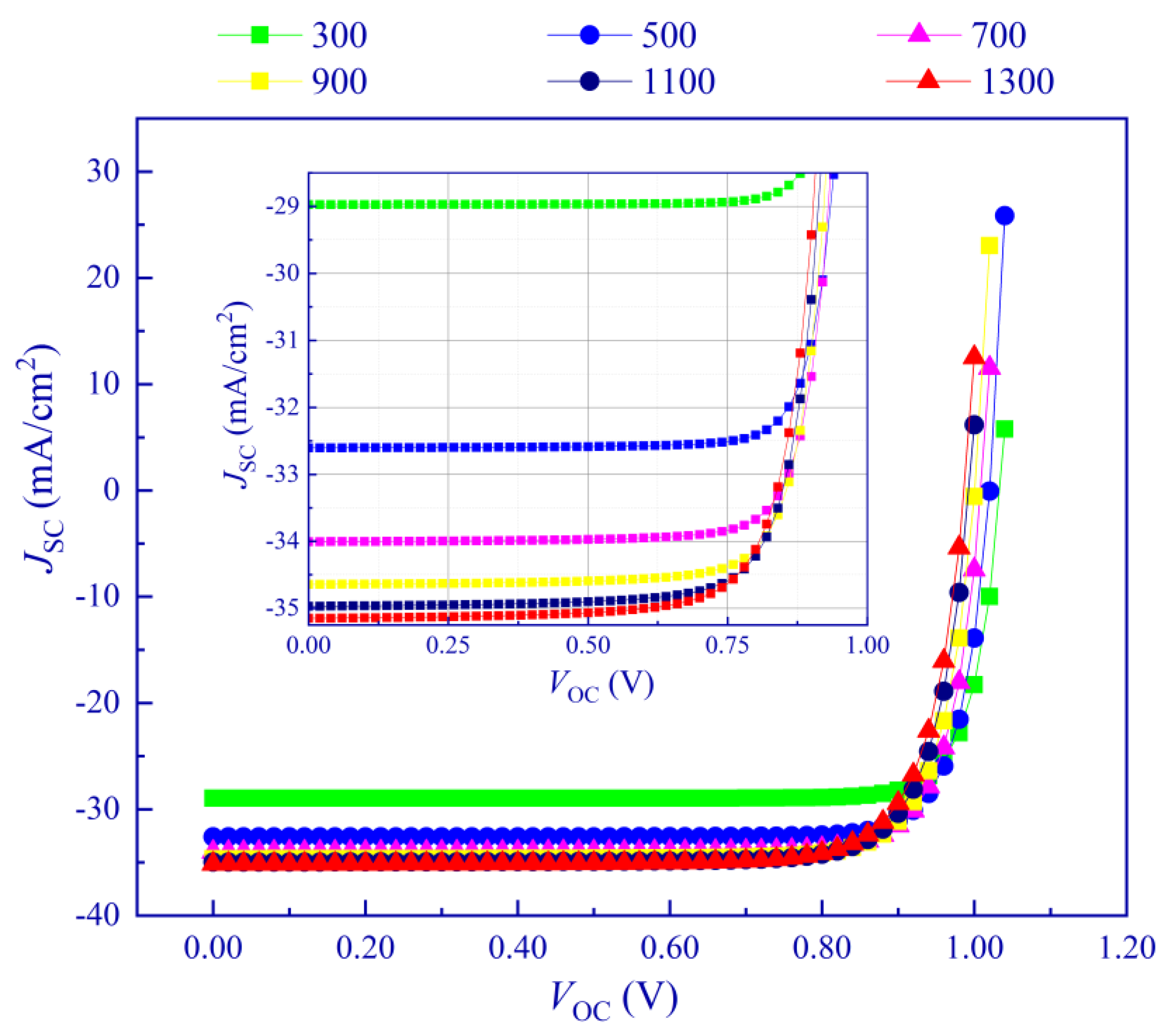
3.6. Influence of the Thickness of the Light-Absorbing Layer on the Device Performance
4. Conclusions
Author Contributions
Funding
Institutional Review Board Statement
Informed Consent Statement
Data Availability Statement
Acknowledgments
Conflicts of Interest
References
- Green, M.A.; Hishikawa, Y.; Dunlop, E.D.; Levi, D.H.; Hohl-Ebinger, J.; Ho-Baillie, A.W.Y. Solar cell efficiency tables (version 52). Prog. Photovolt. Res. Appl. 2018, 26, 427–436. [Google Scholar] [CrossRef]
- Yoshikawa, K.; Kawasaki, H.; Yoshida, W.; Irie, T.; Konishi, K.; Nakano, K.; Uto, T.; Adachi, D.; Kanematsu, M.; Uzu, H.; et al. Silicon heterojunction solar cell with interdigitated back contacts for a photoconversion efficiency over 26%. Nat. Energy 2017, 2, 17032. [Google Scholar] [CrossRef]
- Elsmani, M.I.; Fatima, N.; Jallorina, M.P.A.; Sepeai, S.; Su’ait, M.S.; Ahmad Ludin, N.; Mat Teridi, M.A.; Sopian, K.; Ibrahim, M.A. Recent issues and configuration factors in perovskite-silicon tandem solar cells towards large scaling production. Nanomaterials 2021, 11, 3186. [Google Scholar] [CrossRef] [PubMed]
- Alvarez, H.S.; Silva, A.R.; Espinola, L.C.J.; Vaz, A.R.; Diniz, J.A. NH 4 OH-B silicon texturing of periodic V-groove channels, upright, and inverted pyramids structures. IEEE J. Photovolt. 2021, 11, 570–574. [Google Scholar] [CrossRef]
- Yuan, S.; Cui, Y.; Zhuang, Y.; Chen, P.; Hu, Y.; Yang, B.; Yu, Y.; Ren, Y.; Wang, W.; Chen, W.; et al. Passivated emitter and rear cell silicon solar cells with a front polysilicon passivating contacted selective emitter. Phys. Status Solidi—Rapid Res. Lett. 2021, 15, 2100057. [Google Scholar] [CrossRef]
- Richter, A.; Müller, R.; Benick, J.; Feldmann, F.; Steinhauser, B.; Reichel, C.; Fell, A.; Bivour, M.; Hermle, M.; Glunz, S.W. Design rules for high-efficiency both-sides-contacted silicon solar cells with balanced charge carrier transport and recombination losses. Nat. Energy 2021, 6, 429–438. [Google Scholar] [CrossRef]
- Owusu, P.A.; Asumadu-Sarkodie, S. A review of renewable energy sources, sustainability issues and climate change mitigation. Cogent Eng. 2016, 3, 1167990. [Google Scholar] [CrossRef]
- Ramírez-Márquez, C.; Villicaña-García, E.; Cansino-Loeza, B.; Segovia-Hernández, J.G.; Ponce-Ortega, J.M. Inherent occupational health hazards in the production of solar grade silicon. Process Saf. Environ. Prot. 2020, 142, 285–294. [Google Scholar] [CrossRef]
- Ramírez-Márquez, C.; Contreras-Zarazúa, G.; Martín, M.; Segovia-Hernández, J.G. Safety, economic, and environmental optimization applied to three processes for the production of solar-grade silicon. ACS Sustain. Chem. Eng. 2019, 7, 5355–5366. [Google Scholar] [CrossRef]
- Momblona, C.; Gil-Escrig, L.; Bandiello, E.; Hutter, E.M.; Sessolo, M.; Lederer, K.; Blochwitz-Nimoth, J.; Bolink, H.J. Efficient vacuum deposited p-i-n and n-i-p perovskite solar cells employing doped charge transport layers. Energy Environ. Sci. 2016, 9, 3456–3463. [Google Scholar] [CrossRef]
- Zhao, X.; Sun, Y.; Liu, S.; Chen, G.; Chen, P.; Wang, J.; Cao, W.; Wang, C. Humidity sensitivity behavior of CH3NH3PbI3 perovskite. Nanomaterials 2022, 12, 523. [Google Scholar] [CrossRef] [PubMed]
- Triolo, C.; De Giorgi, M.L.; Lorusso, A.; Cretì, A.; Santangelo, S.; Lomascolo, M.; Anni, M.; Mazzeo, M.; Patané, S. Light emission properties of thermally evaporated CH3NH3PbBr3 perovskite from nano- to macro-scale: Role of free and localized excitons. Nanomaterials 2022, 12, 211. [Google Scholar] [CrossRef] [PubMed]
- Nayak, P.K.; Mahesh, S.; Snaith, H.J.; Cahen, D. Photovoltaic solar cell technologies: Analysing the state of the art. Nat. Rev. Mater. 2019, 4, 269–285. [Google Scholar] [CrossRef]
- Zhou, D.; Zhou, T.; Tian, Y.; Zhu, X.; Tu, Y. Perovskite-based solar cells: Materials, methods, and future perspectives. J. Nanomater. 2018, 2018, 8148072. [Google Scholar] [CrossRef]
- Hwang, T.; Lee, B.; Kim, J.; Lee, S.; Gil, B.; Yun, A.J.; Park, B. From nanostructural evolution to dynamic interplay of constituents: Perspectives for perovskite solar cells. Adv. Mater. 2018, 30, 1704208. [Google Scholar] [CrossRef] [PubMed]
- Yoo, J.J.; Seo, G.; Chua, M.R.; Park, T.G.; Lu, Y.; Rotermund, F.; Kim, Y.-K.; Moon, C.S.; Jeon, N.J.; Correa-Baena, J.-P.; et al. Efficient perovskite solar cells via improved carrier management. Nature 2021, 590, 587–593. [Google Scholar] [CrossRef]
- Li, N.; Niu, X.; Li, L.; Wang, H.; Huang, Z.; Zhang, Y.; Chen, Y.; Zhang, X.; Zhu, C.; Zai, H.; et al. Liquid medium annealing for fabricating durable perovskite solar cells with improved reproducibility. Science 2021, 373, 561–567. [Google Scholar] [CrossRef]
- Lee, K.-M.; Chan, S.-H.; Chiu, W.-H.; Ahn, S.; Ting, C.-C.; Chang, Y.-H.; Suryanarayanan, V.; Wu, M.-C.; Liu, C.-Y. Reducing defects in organic-lead halide perovskite film by delayed thermal annealing combined with KI/I2 for efficient perovskite solar cells. Nanomaterials 2021, 11, 1607. [Google Scholar] [CrossRef]
- Park, H.H. Efficient and stable perovskite solar cells based on inorganic hole transport materials. Nanomaterials 2021, 12, 112. [Google Scholar] [CrossRef]
- Wu, J.; Li, Y.; Li, Y.; Xie, W.; Shi, J.; Li, D.; Cheng, S.; Meng, Q. Using hysteresis to predict the charge recombination properties of perovskite solar cells. J. Mater. Chem. A 2021, 9, 6382–6392. [Google Scholar] [CrossRef]
- Yang, D.; Zhang, G.; Lai, R.; Cheng, Y.; Lian, Y.; Rao, M.; Huo, D.; Lan, D.; Zhao, B.; Di, D. Germanium-lead perovskite light-emitting diodes. Nat. Commun. 2021, 12, 4295. [Google Scholar] [CrossRef] [PubMed]
- Dos Santos Rosa, E.H.; Kowalski, E.L.; Ribeiro Barrozo Toledo, L.F. Simulation of organic solar cells’s power conversion efficiency. Sol. Energy 2021, 221, 483–487. [Google Scholar] [CrossRef]
- Wei, H.; Qiu, P.; Li, Y.; He, Y.; Peng, M.; Zheng, X.; Liu, X. Challenges and strategies of all-inorganic lead-free halide perovskite solar cells. Ceram. Int. 2022, 48, 5876–5891. [Google Scholar] [CrossRef]
- Li, J.; Cao, H.-L.; Jiao, W.-B.; Wang, Q.; Wei, M.; Cantone, I.; Lü, J.; Abate, A. Biological impact of lead from halide perovskites reveals the risk of introducing a safe threshold. Nat. Commun. 2020, 11, 310. [Google Scholar] [CrossRef] [PubMed] [Green Version]
- Montoya De Los Santos, I.; Cortina-Marrero, H.J.; Ruíz-Sánchez, M.A.; Hechavarría-Difur, L.; Sánchez-Rodríguez, F.J.; Courel, M.; Hu, H. Optimization of CH3NH3PbI3 perovskite solar cells: A theoretical and experimental study. Sol. Energy 2020, 199, 198–205. [Google Scholar] [CrossRef]
- Cao, W.; Hu, Z.; Lin, Z.; Guo, X.; Su, J.; Chang, J.; Hao, Y. Defects and doping engineering towards high performance lead-free or lead-less perovskite solar cells. J. Energy Chem. 2022, 68, 420–438. [Google Scholar] [CrossRef]
- Chandra, P.; Mandal, S.K. Morphology controlled (CH3NH3)3Bi2Cl9 thin film for lead free perovskite solar cell. Phys. B Condens. Matter 2022, 625, 413536. [Google Scholar] [CrossRef]
- Bai, F.; Hu, Y.; Hu, Y.; Qiu, T.; Miao, X.; Zhang, S. Lead-free, air-stable ultrathin Cs3Bi2I9 perovskite nanosheets for solar cells. Sol. Energy Mater. Sol. Cells 2018, 184, 15–21. [Google Scholar] [CrossRef]
- Turkevych, I.; Kazaoui, S.; Ito, E.; Urano, T.; Yamada, K.; Tomiyasu, H.; Yamagishi, H.; Kondo, M.; Aramaki, S. Photovoltaic rudorffites: Lead-free silver bismuth halides alternative to hybrid lead halide perovskites. ChemSusChem 2017, 10, 3754–3759. [Google Scholar] [CrossRef]
- Krishnamoorthy, T.; Ding, H.; Yan, C.; Leong, W.L.; Baikie, T.; Zhang, Z.; Sherburne, M.; Li, S.; Asta, M.; Mathews, N.; et al. Lead-free germanium iodide perovskite materials for photovoltaic applications. J. Mater. Chem. A 2015, 3, 23829–23832. [Google Scholar] [CrossRef]
- Ünlü, F.; Deo, M.; Mathur, S.; Kirchartz, T.; Kulkarni, A. Bismuth-based halide perovskite and perovskite-inspired light absorbing materials for photovoltaics. J. Phys. D. Appl. Phys. 2022, 55, 113002. [Google Scholar] [CrossRef]
- Toshniwal, A.; Kheraj, V. Development of organic-inorganic tin halide perovskites: A review. Sol. Energy 2017, 149, 54–59. [Google Scholar] [CrossRef]
- Giustino, F.; Snaith, H.J. Toward lead-free perovskite solar cells. ACS Energy Lett. 2016, 1, 1233–1240. [Google Scholar] [CrossRef] [Green Version]
- Abu Baker, A.M.; Boltaev, G.S.; Iqbal, M.; Pylnev, M.; Hamdan, N.M.; Alnaser, A.S. Giant third-order nonlinear response of mixed perovskite nanocrystals. Materials 2022, 15, 389. [Google Scholar] [CrossRef]
- Pitaro, M.; Tekelenburg, E.K.; Shao, S.; Loi, M.A. Tin halide perovskites: From fundamental properties to solar cells. Adv. Mater. 2022, 34, 2105844. [Google Scholar] [CrossRef]
- Singh, S.; Kabra, D. Comparative study of recombination dynamics in optimized composition of Sn- versus Pb-based perovskite solar cells. ACS Appl. Mater. Interfaces 2021, 13, 42297–42306. [Google Scholar] [CrossRef]
- Roknuzzaman, M.; Ostrikov, K.; Wang, H.; Du, A.; Tesfamichael, T. Towards lead-free perovskite photovoltaics and optoelectronics by ab-initio simulations. Sci. Rep. 2017, 7, 14025. [Google Scholar] [CrossRef]
- Le Corre, V.M.; Stolterfoht, M.; Perdigón Toro, L.; Feuerstein, M.; Wolff, C.; Gil-Escrig, L.; Bolink, H.J.; Neher, D.; Koster, L.J.A. Charge transport layers limiting the efficiency of perovskite solar cells: How to optimize conductivity, doping, and thickness. ACS Appl. Energy Mater. 2019, 2, 6280–6287. [Google Scholar] [CrossRef] [Green Version]
- Braun, S.; Salaneck, W.R.; Fahlman, M. Energy-level alignment at organic/metal and organic/organic interfaces. Adv. Mater. 2009, 21, 1450–1472. [Google Scholar] [CrossRef]
- Deepthi Jayan, K. Design and comparative performance analysis of high-efficiency lead-based and lead-free perovskite solar cells. Phys. Status Solidi 2022, 219, 2100606. [Google Scholar] [CrossRef]
- Deepthi Jayan, K.; Sebastian, V. Modelling and comparative performance analysis of tin based mixed halide perovskite solar cells with IGZO and CuO as charge transport layers. Int. J. Energy Res. 2021, 45, 16618–16632. [Google Scholar] [CrossRef]
- Chen, Q.; Ni, Y.; Dou, X.; Yoshinori, Y. The effect of energy level of transport layer on the performance of ambient air prepared perovskite solar cell: A SCAPS-1D simulation study. Crystals 2022, 12, 68. [Google Scholar] [CrossRef]
- Rombach, F.M.; Haque, S.A.; Macdonald, T.J. Lessons learned from spiro-OMeTAD and PTAA in perovskite solar cells. Energy Environ. Sci. 2021, 14, 5161–5190. [Google Scholar] [CrossRef]
- Mahapatra, B.; Krishna, R.V.; Laxmi; Patel, P.K. Design and optimization of CuSCN/CH3NH3PbI3/TiO2 perovskite solar cell for efficient performance. Opt. Commun. 2022, 504, 127496. [Google Scholar] [CrossRef]
- Farooq, W.; Alshahrani, T.; Kazmi, S.A.A.; Iqbal, J.; Khan, H.A.; Khan, M.; Raja, A.A.; ur Rehman, A. Materials optimization for thin-film copper indium gallium selenide (CIGS) solar cell based on distributed braggs reflector. Optik 2021, 227, 165987. [Google Scholar] [CrossRef]
- Yang, H.-Y.; Rho, W.-Y.; Lee, S.; Kim, S.; Hahn, Y.-B. TiO2 nanoparticles/nanotubes for efficient light harvesting in perovskite solar cells. Nanomaterials 2019, 9, 326. [Google Scholar] [CrossRef] [Green Version]
- Kung, P.; Li, M.; Lin, P.; Chiang, Y.; Chan, C.; Guo, T.; Chen, P. A review of inorganic hole transport materials for perovskite solar cells. Adv. Mater. Interfaces 2018, 5, 1800882. [Google Scholar] [CrossRef]
- Gil, B.; Yun, A.J.; Lee, Y.; Kim, J.; Lee, B.; Park, B. Recent progress in inorganic hole transport materials for efficient and stable perovskite solar cells. Electron. Mater. Lett. 2019, 15, 505–524. [Google Scholar] [CrossRef]
- Arumugam, G.M.; Karunakaran, S.K.; Liu, C.; Zhang, C.; Guo, F.; Wu, S.; Mai, Y. Inorganic hole transport layers in inverted perovskite solar cells: A review. Nano Sel. 2021, 2, 1081–1116. [Google Scholar] [CrossRef]
- Xu, B.; Zhu, H.; Bao, H.; Cao, X.; Dong, Y.; Zhang, Y.; Yin, G.; Li, X.; Wang, S. Bifunctional spiro-fluorene/heterocycle cored hole-transporting materials: Role of the heteroatom on the photovoltaic performance of perovskite solar cells. Chem. Eng. J. 2022, 431, 133371. [Google Scholar] [CrossRef]
- Roy, P.; Raoui, Y.; Khare, A. Design and simulation of efficient tin based perovskite solar cells through optimization of selective layers: Theoretical insights. Opt. Mater. 2022, 125, 112057. [Google Scholar] [CrossRef]
- Singh, N.; Agarwal, A.; Agarwal, M. Performance evaluation of lead–free double-perovskite solar cell. Opt. Mater. 2021, 114, 110964. [Google Scholar] [CrossRef]
- Kanoun, A.-A.; Kanoun, M.B.; Merad, A.E.; Goumri-Said, S. Toward development of high-performance perovskite solar cells based on CH3NH3GeI3 using computational approach. Sol. Energy 2019, 182, 237–244. [Google Scholar] [CrossRef]
- Song, W.; Rakocevic, L.; Thiruvallur Eachambadi, R.; Qiu, W.; Bastos, J.P.; Gehlhaar, R.; Kuang, Y.; Hadipour, A.; Aernouts, T.; Poortmans, J. Improving the morphology stability of spiro-OMeTAD films for enhanced thermal stability of perovskite solar cells. ACS Appl. Mater. Interfaces 2021, 13, 44294–44301. [Google Scholar] [CrossRef] [PubMed]
- Ibanez, J.G.; Rincón, M.E.; Gutierrez-Granados, S.; Chahma, M.; Jaramillo-Quintero, O.A.; Frontana-Uribe, B.A. Conducting polymers in the fields of energy, environmental remediation, and chemical–chiral sensors. Chem. Rev. 2018, 118, 4731–4816. [Google Scholar] [CrossRef] [PubMed]
- Anrango-Camacho, C.; Pavón-Ipiales, K.; Frontana-Uribe, B.A.; Palma-Cando, A. Recent advances in hole-transporting layers for organic solar cells. Nanomaterials 2022, 12, 443. [Google Scholar] [CrossRef]
- Wang, J.; Yu, H.; Hou, C.; Zhang, J. Solution-Processable PEDOT:PSS:α-In 2 Se 3 with enhanced conductivity as a hole transport layer for high-performance polymer solar cells. ACS Appl. Mater. Interfaces 2020, 12, 26543–26554. [Google Scholar] [CrossRef]
- Lee, S.W.; Lee, Y.S.; Heo, J.; Siah, S.C.; Chua, D.; Brandt, R.E.; Kim, S.B.; Mailoa, J.P.; Buonassisi, T.; Gordon, R.G. Improved Cu2O-based solar cells using atomic layer deposition to control the Cu oxidation state at the p-n junction. Adv. Energy Mater. 2014, 4, 1301916. [Google Scholar] [CrossRef]
- Murali, D.S.; Kumar, S.; Choudhary, R.J.; Wadikar, A.D.; Jain, M.K.; Subrahmanyam, A. Synthesis of Cu2O from CuO thin films: Optical and electrical properties. AIP Adv. 2015, 5, 047143. [Google Scholar] [CrossRef]
- Scanlon, D.O.; Morgan, B.J.; Watson, G.W.; Walsh, A. Acceptor levels in p-Type Cu2O: Rationalizing theory and experiment. Phys. Rev. Lett. 2009, 103, 096405. [Google Scholar] [CrossRef]
- Zuo, C.; Ding, L. Solution-processed Cu2O and CuO as hole transport materials for efficient perovskite solar cells. Small 2015, 11, 5528–5532. [Google Scholar] [CrossRef] [PubMed]
- He, Y.; Xu, L.; Yang, C.; Guo, X.; Li, S. Design and numerical investigation of a lead-free inorganic layered double perovskite Cs4CuSb2Cl12 nanocrystal solar cell by SCAPS-1D. Nanomaterials 2021, 11, 2321. [Google Scholar] [CrossRef] [PubMed]
- Samiul Islam, M.; Sobayel, K.; Al-Kahtani, A.; Islam, M.A.; Muhammad, G.; Amin, N.; Shahiduzzaman, M.; Akhtaruzzaman, M. Defect study and modelling of SnX3-based perovskite solar cells with SCAPS-1D. Nanomaterials 2021, 11, 1218. [Google Scholar] [CrossRef] [PubMed]
- Yao, H.; Liu, L. Design and optimize the performance of self-powered photodetector based on PbS/TiS3 heterostructure by SCAPS-1D. Nanomaterials 2022, 12, 325. [Google Scholar] [CrossRef]
- Moiz, S.A. Optimization of hole and electron transport layer for highly efficient lead-free Cs2TiBr6-based perovskite solar cell. Photonics 2021, 9, 23. [Google Scholar] [CrossRef]
- Piñón Reyes, A.C.; Ambrosio Lázaro, R.C.; Monfil Leyva, K.; Luna López, J.A.; Flores Méndez, J.; Heredia Jiménez, A.H.; Muñoz Zurita, A.L.; Severiano Carrillo, F.; Ojeda Durán, E. Study of a lead-free perovskite solar cell using CZTS as HTL to achieve a 20% PCE by SCAPS-1D simulation. Micromachines 2021, 12, 1508. [Google Scholar] [CrossRef]
- Zyoud, S.H.; Zyoud, A.H.; Ahmed, N.M.; Prasad, A.R.; Khan, S.N.; Abdelkader, A.F.I.; Shahwan, M. Numerical modeling of high conversion efficiency FTO/ZnO/CdS/CZTS/MO thin film-based solar cells: Using SCAPS-1D software. Crystals 2021, 11, 1468. [Google Scholar] [CrossRef]
- Mottakin, M.; Sobayel, K.; Sarkar, D.; Alkhammash, H.; Alharthi, S.; Techato, K.; Shahiduzzaman, M.; Amin, N.; Sopian, K.; Akhtaruzzaman, M. Design and modelling of eco-friendly CH3NH3SnI3-based perovskite solar cells with suitable transport layers. Energies 2021, 14, 7200. [Google Scholar] [CrossRef]
- Raoui, Y.; Ez-Zahraouy, H.; Tahiri, N.; El Bounagui, O.; Ahmad, S.; Kazim, S. Performance analysis of MAPbI3 based perovskite solar cells employing diverse charge selective contacts: Simulation study. Sol. Energy 2019, 193, 948–955. [Google Scholar] [CrossRef]
- Lin, L.; Jiang, L.; Li, P.; Xiong, H.; Kang, Z.; Fan, B.; Qiu, Y. Simulated development and optimized performance of CsPbI3 based all-inorganic perovskite solar cells. Sol. Energy 2020, 198, 454–460. [Google Scholar] [CrossRef]
- Patel, P.K. Device simulation of highly efficient eco-friendly CH3NH3SnI3 perovskite solar cell. Sci. Rep. 2021, 11, 3082. [Google Scholar] [CrossRef] [PubMed]
- Rono, N.; Merad, A.E.; Kibet, J.K.; Martincigh, B.S.; Nyamori, V.O. A theoretical investigation of the effect of the hole and electron transport materials on the performance of a lead-free perovskite solar cell based on CH3NH3SnI3. J. Comput. Electron. 2021, 20, 993–1005. [Google Scholar] [CrossRef]
- Chen, M.; Ju, M.-G.; Garces, H.F.; Carl, A.D.; Ono, L.K.; Hawash, Z.; Zhang, Y.; Shen, T.; Qi, Y.; Grimm, R.L.; et al. Highly stable and efficient all-inorganic lead-free perovskite solar cells with native-oxide passivation. Nat. Commun. 2019, 10, 16. [Google Scholar] [CrossRef] [PubMed] [Green Version]
- Abd Mutalib, M.; Ahmad Ludin, N.; Nik Ruzalman, N.A.A.; Barrioz, V.; Sepeai, S.; Mat Teridi, M.A.; Su’ait, M.S.; Ibrahim, M.A.; Sopian, K. Progress towards highly stable and lead-free perovskite solar cells. Mater. Renew. Sustain. Energy 2018, 7, 7. [Google Scholar] [CrossRef] [Green Version]
- Tailor, N.K.; Kar, S.; Mishra, P.; These, A.; Kupfer, C.; Hu, H.; Awais, M.; Saidaminov, M.; Dar, M.I.; Brabec, C.; et al. Advances in lead-free perovskite single crystals: Fundamentals and applications. ACS Mater. Lett. 2021, 3, 1025–1080. [Google Scholar] [CrossRef]
- ABENA, A.M.N.; NGOUPO, A.T.; ABEGA, F.X.A.; NDJAKA, J.M.B. Numerical investigation of solar cells based on hybrid organic cation perovskite with inorganic HTL via SCAPS-1D. Chinese J. Phys. 2022, 76, 94–109. [Google Scholar] [CrossRef]
- Al-Hattab, M.; Moudou, L.; Khenfouch, M.; Bajjou, O.; Chrafih, Y.; Rahmani, K. Numerical simulation of a new heterostructure CIGS/GaSe solar cell system using SCAPS-1D software. Sol. Energy 2021, 227, 13–22. [Google Scholar] [CrossRef]
- Houimi, A.; Gezgin, S.Y.; Mercimek, B.; Kılıç, H.Ş. Numerical analysis of CZTS/n-Si solar cells using SCAPS-1D. A comparative study between experimental and calculated outputs. Opt. Mater. 2021, 121, 111544. [Google Scholar] [CrossRef]
- Moiz, S.A.; Alahmadi, A.N.M. Design of dopant and lead-free novel perovskite solar cell for 16.85% efficiency. Polymers 2021, 13, 2110. [Google Scholar] [CrossRef]
- Burgelman, M.; Decock, K.; Khelifi, S.; Abass, A. Advanced electrical simulation of thin film solar cells. Thin Solid Films 2013, 535, 296–301. [Google Scholar] [CrossRef]
- Verschraegen, J.; Burgelman, M. Numerical modeling of intra-band tunneling for heterojunction solar cells in scaps. Thin Solid Films 2007, 515, 6276–6279. [Google Scholar] [CrossRef]
- Hao, L.; Zhou, M.; Song, Y.; Ma, X.; Wu, J.; Zhu, Q.; Fu, Z.; Liu, Y.; Hou, G.; Li, T. Tin-based perovskite solar cells: Further improve the performance of the electron transport layer-free structure by device simulation. Sol. Energy 2021, 230, 345–354. [Google Scholar] [CrossRef]
- Deepthi Jayan, K.; Sebastian, V. Comprehensive device modelling and performance analysis of MASnI3 based perovskite solar cells with diverse ETM, HTM and back metal contacts. Sol. Energy 2021, 217, 40–48. [Google Scholar] [CrossRef]
- Ito, N.; Kamarudin, M.A.; Hirotani, D.; Zhang, Y.; Shen, Q.; Ogomi, Y.; Iikubo, S.; Minemoto, T.; Yoshino, K.; Hayase, S. Mixed Sn–Ge perovskite for enhanced perovskite solar cell performance in air. J. Phys. Chem. Lett. 2018, 9, 1682–1688. [Google Scholar] [CrossRef]
- Minemoto, T.; Kawano, Y.; Nishimura, T.; Shen, Q.; Yoshino, K.; Iikubo, S.; Hayase, S.; Chantana, J. Theoretical analysis of band alignment at back junction in Sn–Ge perovskite solar cells with inverted p-i-n structure. Sol. Energy Mater. Sol. Cells 2020, 206, 110268. [Google Scholar] [CrossRef]
- Noel, N.K.; Abate, A.; Stranks, S.D.; Parrott, E.S.; Burlakov, V.M.; Goriely, A.; Snaith, H.J. Enhanced photoluminescence and solar cell performance via lewis base passivation of organic–inorganic lead halide perovskites. ACS Nano 2014, 8, 9815–9821. [Google Scholar] [CrossRef]
- Kearney, K.; Seo, G.; Matsushima, T.; Adachi, C.; Ertekin, E.; Rockett, A. Computational analysis of the interplay between deep level traps and perovskite solar cell efficiency. J. Am. Chem. Soc. 2018, 140, 15655–15660. [Google Scholar] [CrossRef]
- Joshi, P.H.; Zhang, L.; Hossain, I.M.; Abbas, H.A.; Kottokkaran, R.; Nehra, S.P.; Dhaka, M.; Noack, M.; Dalal, V.L. The physics of photon induced degradation of perovskite solar cells. AIP Adv. 2016, 6, 115114. [Google Scholar] [CrossRef] [Green Version]
- Adinolfi, V.; Yuan, M.; Comin, R.; Thibau, E.S.; Shi, D.; Saidaminov, M.I.; Kanjanaboos, P.; Kopilovic, D.; Hoogland, S.; Lu, Z.-H.; et al. The in-gap electronic state spectrum of methylammonium lead iodide single-crystal perovskites. Adv. Mater. 2016, 28, 3406–3410. [Google Scholar] [CrossRef]
- De Quilettes, D.W.; Vorpahl, S.M.; Stranks, S.D.; Nagaoka, H.; Eperon, G.E.; Ziffer, M.E.; Snaith, H.J.; Ginger, D.S. Impact of microstructure on local carrier lifetime in perovskite solar cells. Science 2015, 348, 683–686. [Google Scholar] [CrossRef] [Green Version]
- Chowdhury, M.S.; Shahahmadi, S.A.; Chelvanathan, P.; Tiong, S.K.; Amin, N.; Techato, K.; Nuthammachot, N.; Chowdhury, T.; Suklueng, M. Effect of deep-level defect density of the absorber layer and n/i interface in perovskite solar cells by SCAPS-1D. Results Phys. 2020, 16, 102839. [Google Scholar] [CrossRef]
- Walukiewicz, W.; Rey-Stolle, I.; Han, G.; Jaquez, M.; Broberg, D.; Xie, W.; Sherburne, M.; Mathews, N.; Asta, M. Bistable amphoteric native defect model of perovskite photovoltaics. J. Phys. Chem. Lett. 2018, 9, 3878–3885. [Google Scholar] [CrossRef] [PubMed] [Green Version]
- Jiang, Q.; Zhao, Y.; Zhang, X.; Yang, X.; Chen, Y.; Chu, Z.; Ye, Q.; Li, X.; Yin, Z.; You, J. Surface passivation of perovskite film for efficient solar cells. Nat. Photonics 2019, 13, 460–466. [Google Scholar] [CrossRef]
- Yoo, J.J.; Wieghold, S.; Sponseller, M.C.; Chua, M.R.; Bertram, S.N.; Hartono, N.T.P.; Tresback, J.S.; Hansen, E.C.; Correa-Baena, J.-P.; Bulović, V.; et al. An interface stabilized perovskite solar cell with high stabilized efficiency and low voltage loss. Energy Environ. Sci. 2019, 12, 2192–2199. [Google Scholar] [CrossRef] [Green Version]
- Zheng, X.; Chen, B.; Dai, J.; Fang, Y.; Bai, Y.; Lin, Y.; Wei, H.; Zeng, X.C.; Huang, J. Defect passivation in hybrid perovskite solar cells using quaternary ammonium halide anions and cations. Nat. Energy 2017, 2, 17102. [Google Scholar] [CrossRef]
- Wolff, C.M.; Caprioglio, P.; Stolterfoht, M.; Neher, D. Nonradiative recombination in perovskite solar cells: The role of interfaces. Adv. Mater. 2019, 31, 1902762. [Google Scholar] [CrossRef] [Green Version]
- Samantaray, M.R.; Rana, N.K.; Kumar, A.; Ghosh, D.S.; Chander, N. Stability study of large-area perovskite solar cells fabricated with copper as low-cost metal contact. Int. J. Energy Res. 2022, 46, 1250–1262. [Google Scholar] [CrossRef]
- Çaldıran, Z. Modification of Schottky barrier height using an inorganic compound interface layer for various contact metals in the metal/p-Si device structure. J. Alloys Compd. 2021, 865, 158856. [Google Scholar] [CrossRef]
- Lin, C.-H.; Li, T.-Y.; Cheng, B.; Liu, C.; Yang, C.-W.; Ke, J.-J.; Wei, T.-C.; Li, L.-J.; Fratalocchi, A.; He, J.-H. Metal contact and carrier transport in single crystalline CH3NH3PbBr3 perovskite. Nano Energy 2018, 53, 817–827. [Google Scholar] [CrossRef] [Green Version]
- Zai, H.; Ma, Y.; Chen, Q.; Zhou, H. Ion migration in halide perovskite solar cells: Mechanism, characterization, impact and suppression. J. Energy Chem. 2021, 63, 528–549. [Google Scholar] [CrossRef]
- Cheng, Y.; Liu, X.; Guan, Z.; Li, M.; Zeng, Z.; Li, H.; Tsang, S.; Aberle, A.G.; Lin, F. Revealing the degradation and self-healing mechanisms in perovskite solar cells by sub-bandgap external quantum efficiency spectroscopy. Adv. Mater. 2021, 33, 2006170. [Google Scholar] [CrossRef] [PubMed]
- Roy, P.; Tiwari, S.; Khare, A. An investigation on the influence of temperature variation on the performance of tin (Sn) based perovskite solar cells using various transport layers and absorber layers. Results Opt. 2021, 4, 100083. [Google Scholar] [CrossRef]
- Jiang, X.; Li, H.; Zhou, Q.; Wei, Q.; Wei, M.; Jiang, L.; Wang, Z.; Peng, Z.; Wang, F.; Zang, Z.; et al. One-step synthesis of SnI 2·(DMSO) x adducts for high-performance tin perovskite solar cells. J. Am. Chem. Soc. 2021, 143, 10970–10976. [Google Scholar] [CrossRef] [PubMed]


| Parameters | FTO | TiO2 | CH3NH3SnI3 | Spiro-OMeTAD | PEDOT:PSS | Cu2O |
|---|---|---|---|---|---|---|
| Thickness (nm) | 500 | 50 * | 300–1300 * | 50 * | 50 * | 50 * |
| Band gap (eV) | 3.50 | 3.20 | 1.30 | 3.06 | 1.80 | 2.17 |
| Electron affinity (eV) | 4.00 | 4.26 | 4.17 | 2.05 | 3.40 | 3.20 |
| Relative dielectric permittivity | 9.00 | 9.00 | 8.20 | 3.00 | 18.00 | 7.10 |
| Conduction band effective density of states (cm−3) | 2.20 × 10¹⁸ | 2.20 × 10¹⁸ | 1 × 10¹⁸ | 2.20 × 10¹⁸ | 2.20 × 10¹⁸ | 2.00 × 10¹⁷ |
| Valence band effective density of states (cm−3) | 1.80 × 10¹⁹ | 1.80 × 10¹⁹ | 1 × 10¹⁸ | 1.80 × 10¹⁹ | 1.80 × 10¹⁹ | 1.10 × 10¹⁹ |
| Electron thermal velocity (cm/s) | 107 | 107 | 107 | 107 | 107 | 107 |
| Hole thermal velocity (cm/s) | 107 | 107 | 107 | 107 | 107 | 107 |
| Electron mobility (cm2/Vs) | 20.00 | 20.00 | 1.60 | 2.00 × 10⁻⁴ | 4.50 × 10⁻² | 200.00 |
| Hole mobility (cm2/Vs) | 10.00 | 10.00 | 1.60 | 2.00 × 10⁻⁴ | 4.50 × 10⁻² | 80.00 |
| Shallow donor density ND (cm−3) | 2.00 × 10¹⁹ | 1018 | 0 | 0 | 0 | 0 |
| Shallow acceptor density NA (cm−3) | 0 | 0 | 1.00 × 10¹⁴ | 1.00 × 10¹⁸ | 1.00 × 10²⁰ | 1.00 × 10¹⁸ |
| References | [53,82] | [83] | [82,83] | [53] | [84,85] | [53,83] |
Publisher’s Note: MDPI stays neutral with regard to jurisdictional claims in published maps and institutional affiliations. |
© 2022 by the authors. Licensee MDPI, Basel, Switzerland. This article is an open access article distributed under the terms and conditions of the Creative Commons Attribution (CC BY) license (https://creativecommons.org/licenses/by/4.0/).
Share and Cite
Omarova, Z.; Yerezhep, D.; Aldiyarov, A.; Tokmoldin, N. In Silico Investigation of the Impact of Hole-Transport Layers on the Performance of CH3NH3SnI3 Perovskite Photovoltaic Cells. Crystals 2022, 12, 699. https://0-doi-org.brum.beds.ac.uk/10.3390/cryst12050699
Omarova Z, Yerezhep D, Aldiyarov A, Tokmoldin N. In Silico Investigation of the Impact of Hole-Transport Layers on the Performance of CH3NH3SnI3 Perovskite Photovoltaic Cells. Crystals. 2022; 12(5):699. https://0-doi-org.brum.beds.ac.uk/10.3390/cryst12050699
Chicago/Turabian StyleOmarova, Zhansaya, Darkhan Yerezhep, Abdurakhman Aldiyarov, and Nurlan Tokmoldin. 2022. "In Silico Investigation of the Impact of Hole-Transport Layers on the Performance of CH3NH3SnI3 Perovskite Photovoltaic Cells" Crystals 12, no. 5: 699. https://0-doi-org.brum.beds.ac.uk/10.3390/cryst12050699