
High-Efficiency p-n Homojunction Perovskite and CIGS Tandem Solar Cell


1
Faculty of Electrical Engineering, Shahid Rajaee Teacher Training University, Tehran 16788-15811, Iran
2
Nano-Photonics and Optoelectronics Research Laboratory (NORLab), Shahid Rajaee Teacher Training University, Tehran 16788-15811, Iran
*
Author to whom correspondence should be addressed.
Crystals 2022, 12(5), 703; https://0-doi-org.brum.beds.ac.uk/10.3390/cryst12050703
Submission received: 17 March 2022
/
Revised: 10 May 2022
/
Accepted: 13 May 2022
/
Published: 15 May 2022
(This article belongs to the Topic Electrolyte Design and Interface Engineering toward Safer Energy Storage)
Abstract
:Efficiency has been known to be one of the most important factors in a solar cell. This article presents the results of a simulation performed on a perovskite/CIGS dual-junction solar cell. In this report, first, a top solar cell consisting of a perovskite absorber layer is simulated using the pn-junction; the separation and transfer of carriers in this structure are done by the internal electric field. The pn-junction has a discharge area smaller than the pin-junction, which increases carrier recombination and reduces optical losses. The perovskite band gap of 1.9 eV is considered, and the efficiency is 21.65% using the Au electrode. Then, the bottom solar cell is fabricated with a CIGS absorbent layer with a 1.4 eV band gap and an efficiency of 11.46%. After simulating and evaluating the performance of the top and bottom solar cells independently, both cells were simulated and examined for the dual-junction state. Since the perovskite and CIGS band gaps are both adjustable, these two materials can act as a proper partner for an absorbent layer in a dual-junction solar cell. In this structure, instead of the usual connection of p-i-n and n-i-p perovskite, n-type and p-type homojunction perovskite connection is used, in which the transfer and separation of carriers are done by an internal electric field. Due to the fact that in this structure, the discharge area is smaller, the recombination of carriers is increased, and the light losses are reduced, which will increase the absorption and efficiency of the cell. The results show that in the tandem design, we encounter an increase in Voc (2.25 V), thus increasing the efficiency of the solar cell (30.71%).
1. Introduction
Perovskite as an absorbent layer in solar cells was first reported by Miyasaka et al. in 2009 [1]. It has been widely used in the manufacture of solar cells since the perovskite became known [2,3,4,5,6,7,8,9,10,11,12,13]. The high mobility of the carriers, the easy manufacturing process, and the great light absorption in the visible area make perovskite a light active layer in the solar cell. CIGS (Copper Indium Gallium Selenide) also has a very high absorption coefficient, which is greater than across the visible spectrum [14]. The general formula for the CIGS layer is CuIn(1−x)GaxSe2, where X specifies the Ga value in the composition. By adding a small amount of gallium to the CIS (Copper Indium Selenide) layer, its band gap can be increased from the normal value of 1 eV to 1.7 eV [15].
One of the advantages of a dual-junction solar cell compared to a single-junction solar cell is the spectral response. In dual-junction cells, the spectral response is equal to the sum of its two sub-cells. Therefore, a dual-junction solar cell is capable of absorbing a wide range of sunlight. According to the theory of multicellular cells, open circuit voltage is equal to the sum of the open-circuit voltages of single-junction cells and short-circuit current is equal to the minimum short-circuit current of single-junction cells [16]. In multi-junction solar cells, the low wavelengths of sunlight are absorbed by the first layer, and the higher wavelengths are absorbed by the next layers, respectively [17,18].
The structure of most perovskite-based solar cells is p-i-n or n-i-p. However, a comparison has been recently made between homojunction and heterojunction perovskite architectures, in which the pn homojunction architectures, solar cell efficiency is 23%, which has increased significantly compared to heterojunction architectures [19].
In 2019, the use of Au nanoparticles with a radius of 60 nm increased the absorption in the structure of the perovskite solar cell [20]. In 2020, the CGS/CIGS dual-junction solar cell was simulated with and without gallium, and its yield was 32.3% [21].
In 2021, work was carried out on perovskite dual-junction structures with various compounds, including CIGS, which then led to an efficiency of 25%. The performance of all compounds is compared [22]. Recently, an inorganic perovskite/organic tandem solar cell has been developed, the of which has been increased using the /ZnO electron transfer layer, with an efficiency of 20.18% [23].
Furthermore, dual-junction perovskite/CIGS and perovskite/Si solar cells with a 4-terminal architecture were designed and experimented, with a reported efficiency of 25.0% and 25.7%, respectively [24]. Recently, a perovskite/perovskite dual-junction solar cell was simulated and experimented with Pb-free perovskite () and low Pb perovskite (FACs), with a 2-terminal architecture having an efficiency of 17.35% [25]. In this report, among the various perovskite, Methylammonium lead halides is considered for simulation. This simulation was performed at 300 K temperature.
The rest of the paper is written as follows: Section 2 deals with the simulation method and its equations. The general schematic of the solar cell and the table of parameters required for simulation are also given. In Section 3, the perovskite single-junction solar cell, the CIGS single-junction solar cell, and the integration of top and bottom cells and comparison of the results with single-junction modes are simulated. Finally, a conclusion is drawn in the last section.
2. Materials and Methods
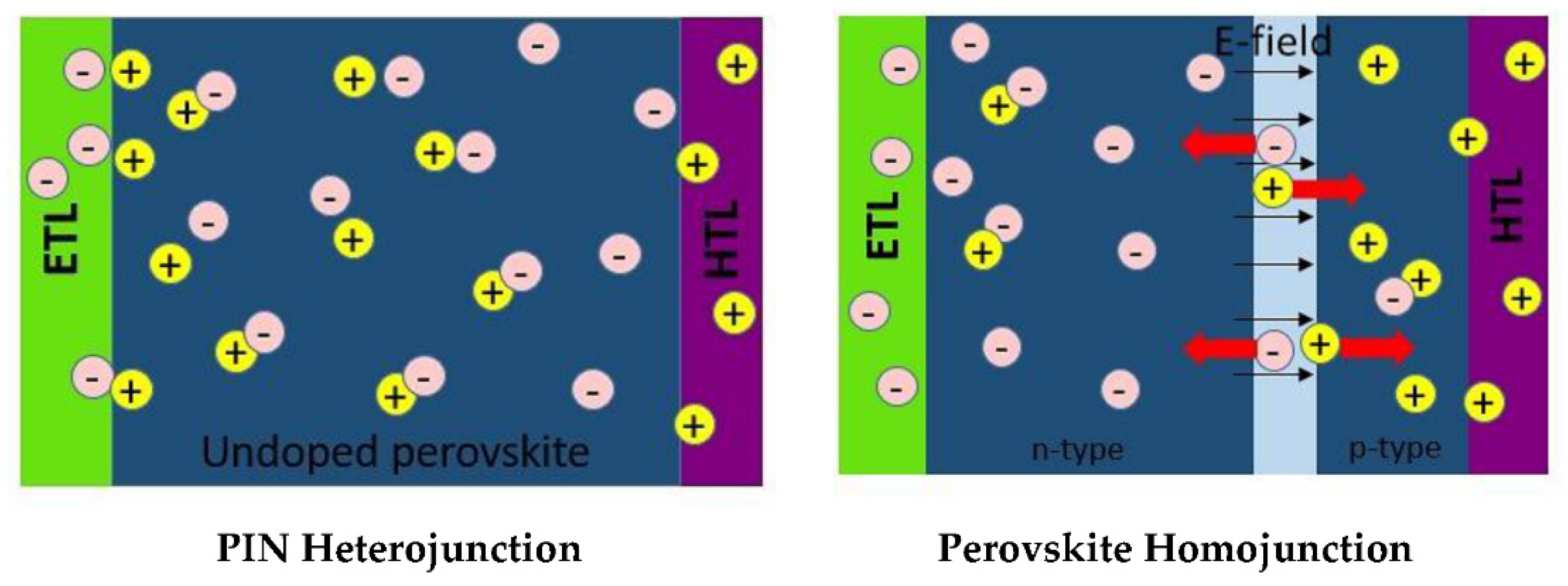
Perovskite solar cell is a top cell. The perovskite solar cell is simulated as a p-n diode junction. In this method, the separation and transfer of carriers is the responsibility of the internal electric field. It also reduces light losses and increases the recombination of carriers [19,26,27,28,29]. Accordingly, two layers of n- and p-type perovskite have been used. Two-hole transfer layer (HTL) and electron transfer layer (ETL) have been placed above and below them. Figure 1 shows carriers in generation and transport in the homojunction and heterojunction perovskite solar cell.
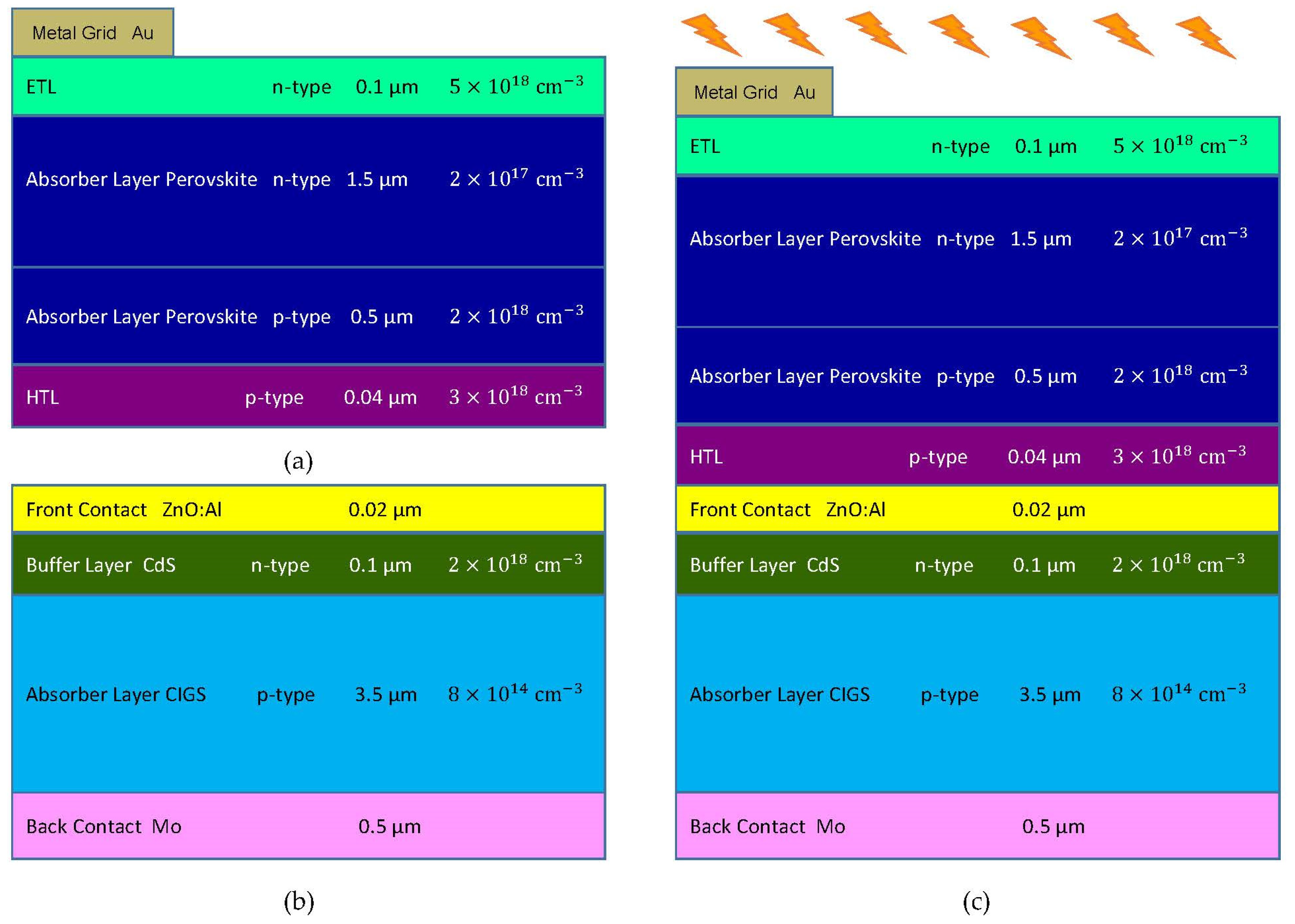
The lower absorbent cell layer is CIGS. In 4-terminal architecture, there is no need for current matching and tunnel junction. In this report, the top and bottom cells are connected in 4-terminals. According to this configuration, two cells are parallel, so 4 electrodes are needed. The general schematic of the structure of the perovskite single-junction solar cell (Figure 2a), the CIGS single-junction solar cell (Figure 2b), and the dual-junction perovskite/CIGS solar cell (Figure 2c) are shown in Figure 2.
Three main numerical solution methods are the GUMMEL method, the NEWTON method, and the BLOCK method. The GUMMEL method is used for equations of a weakly coupled system with linear convergence. The NEWTON method is used for the equations of a strong coupling system with a second-order convergence, in which case the software takes a long time to solve the equations to create a reliable convergence. Finally, the BLOCK method performs rapid simulations [28]. In this simulation, partial differential equations (PDEs) have been utilized to model the cell using Newton’s numerical solution.
The function of the solar cell can be evaluated by simultaneously solving the three main equations of Poisson, the continuity and the transfer of carriers [29]. In general, Poisson’s equation can be written as follows [30]:
where E is the electric field, is the density of the charge space, and is the semiconductor transmission coefficient. The equations of electron and hole continuity in stable conditions are [31]:
In Equations (2) and (3), n and p are the density of free electrons and holes, q is the charge of electrons, and are the electron and hole current density, and are the rate of electron and hole production, and are the recombination rate of electrons and holes specifies, respectively.
The carrier transfer current equation is as follows [32]:
where and are the mobility of electrons and holes, and and are the diffusion coefficients of electrons and holes, respectively. The total transfer current is obtained from the sum of Equations (4) and (5):
In this process, the Shockley-Reed-Hall recombination method has been used to consider the production recombination effect of carriers [33]. Moreover, in this simulation, for the distribution of electron density and cavities, the Dirac-Fermi distribution function at a temperature of K according to Equation (7) has been used [34]:
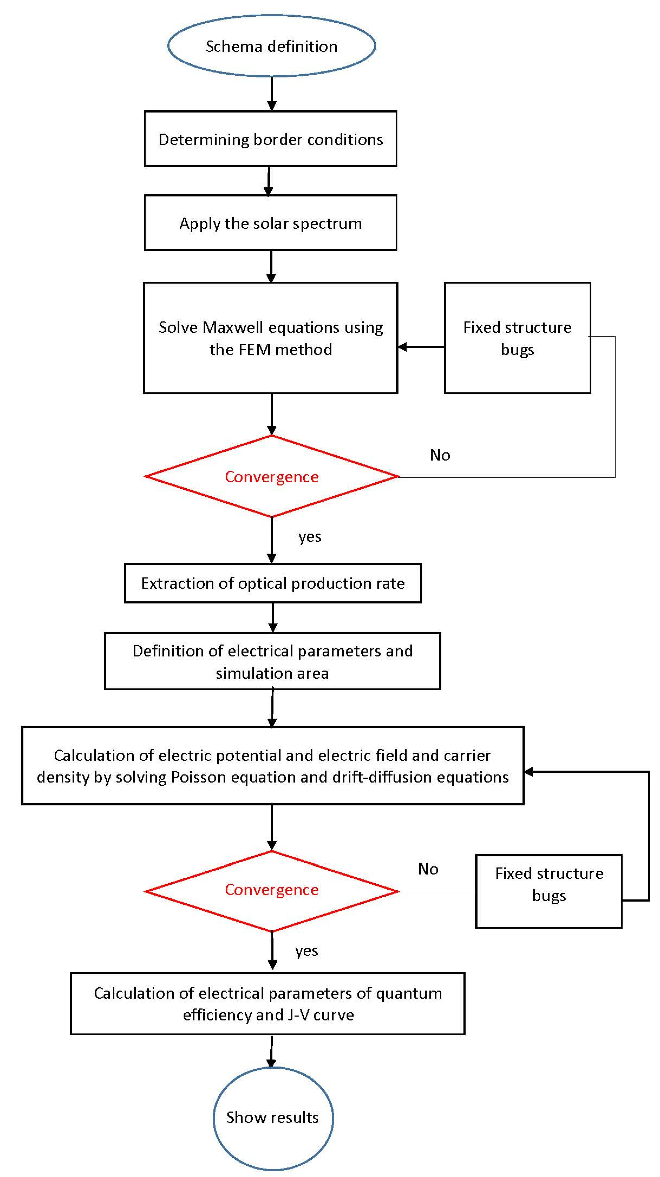
Here, K is the constant of Boltzmann, T is the absolute temperature in Kelvin, and is the form of surface energy. In this simulation, the finite element method (FEM) using the Newton iterative algorithm method is used. The basis of this method is either the complete elimination of differential equations or their simplification to ordinary differential equations, which are solved by numerical methods such as Euler. The flowchart of the general simulation process is given in Appendix A. The parameters required to simulate the Perovskite/CIGS dual-junction solar cell are also listed in Table 1, and some of these parameters were reported in [35,36].
3. Results and Discussion
This section is divided into three parts: Section 3.1 simulates the perovskite single-junction solar cell. Section 3.2 presents the CIGS single-junction solar cell simulation. Section 3.3 simulates the integration of top and bottom cells and compares the results with single-junction modes [37].
3.1. Perovskite Top Cell
In this section, we first examine the results obtained from the simulation of a single-junction perovskite solar cell, which is the top cell of the dual-junction structure. The specifications of this cell are shown in Figure 2, and the relevant parameters are presented in Table 1.
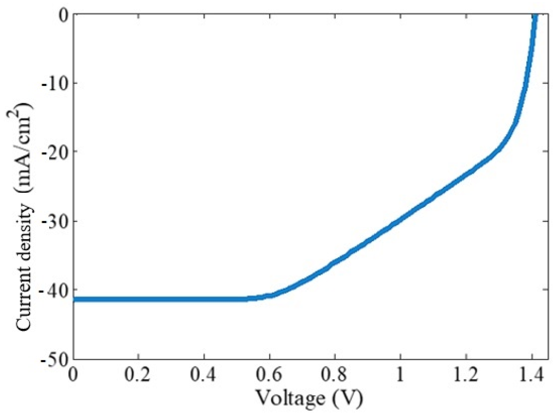
Figure 3 shows solar cell band structure including HTL layer with a thickness of 0.04 μm and an impurity density of 3 cm−3 p-type, perovskite layer with a thickness of 0.5 μm and a density of cm−3 p-type, a thickness of a layer of perovskite 1.5 μm and impurity density cm−3 n-types, and finally, an ETL layer with a thickness of 0.1 μm and impurity density of cm−3 n-type. The black curve shows the conduction band, and the red curve shows the valence band. Figure 4 illustrates the J-V characteristic of a single-junction perovskite solar cell. The main parameters of the cell can be calculated by the assistance of this diagram.
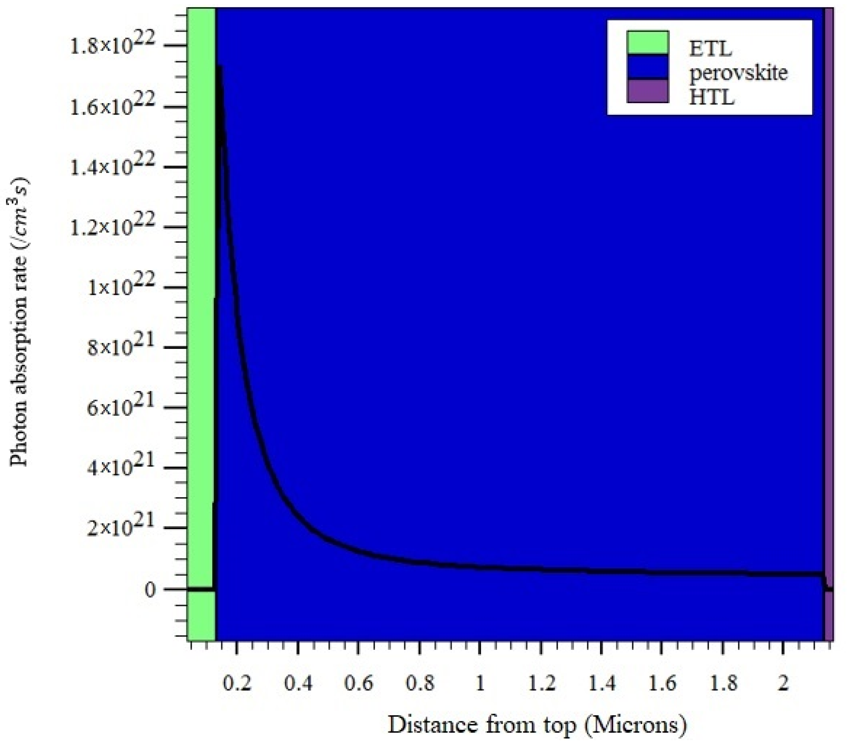
The number of photons absorbed per area unit of the solar cell per time unit is plotted according to the wavelength for the perovskite single-junction solar cell in Figure 5. As can be concluded from the figure, the highest cell absorption efficiency occurred in the perovskite layer. The output parameters obtained from the top cell (perovskite) are given in Table 2. Due to the fact that in the top cell (perovskite), instead of the p-i-n heterojunction, the p-n homojunction is used, and the tunnel junction is considered ideal; as a result, it passes the whole flow and has no losses.
In the homojunction perovskite structure, due to the presence of an internal electric field, the recombination rate of the carriers is lower. Therefore, a reduction in electron concentration causes an increase in free holes of the p-type region of perovskite, which moves the region away from the interface and improves cell performance.
3.2. CIGS Bottom Cell
In this section, the simulation of the lower solar cell (CIGS) is discussed separately. The CIGS solar cell is simulated as a p-n diode junction. So, ZnO:Al as front contact, CIGS type n is used as the absorbent layer and CdS type p is used as the buffer layer with the Mo back contact layer underneath. The top electrode is considered ideal.
Cu() has a variable energy gap from 1.04 eV to 1.68 eV. The increase in the energy gap of an absorbent and thus the rise in the gallium content is determined by:
The relationship between the energy gap and the value of x, which represents the content of gallium, is expressed as [37,38]:
In this study, the value of x is considered 0.7, and according to Equation (9), the value of the band gap of 1.4 eV is obtained.
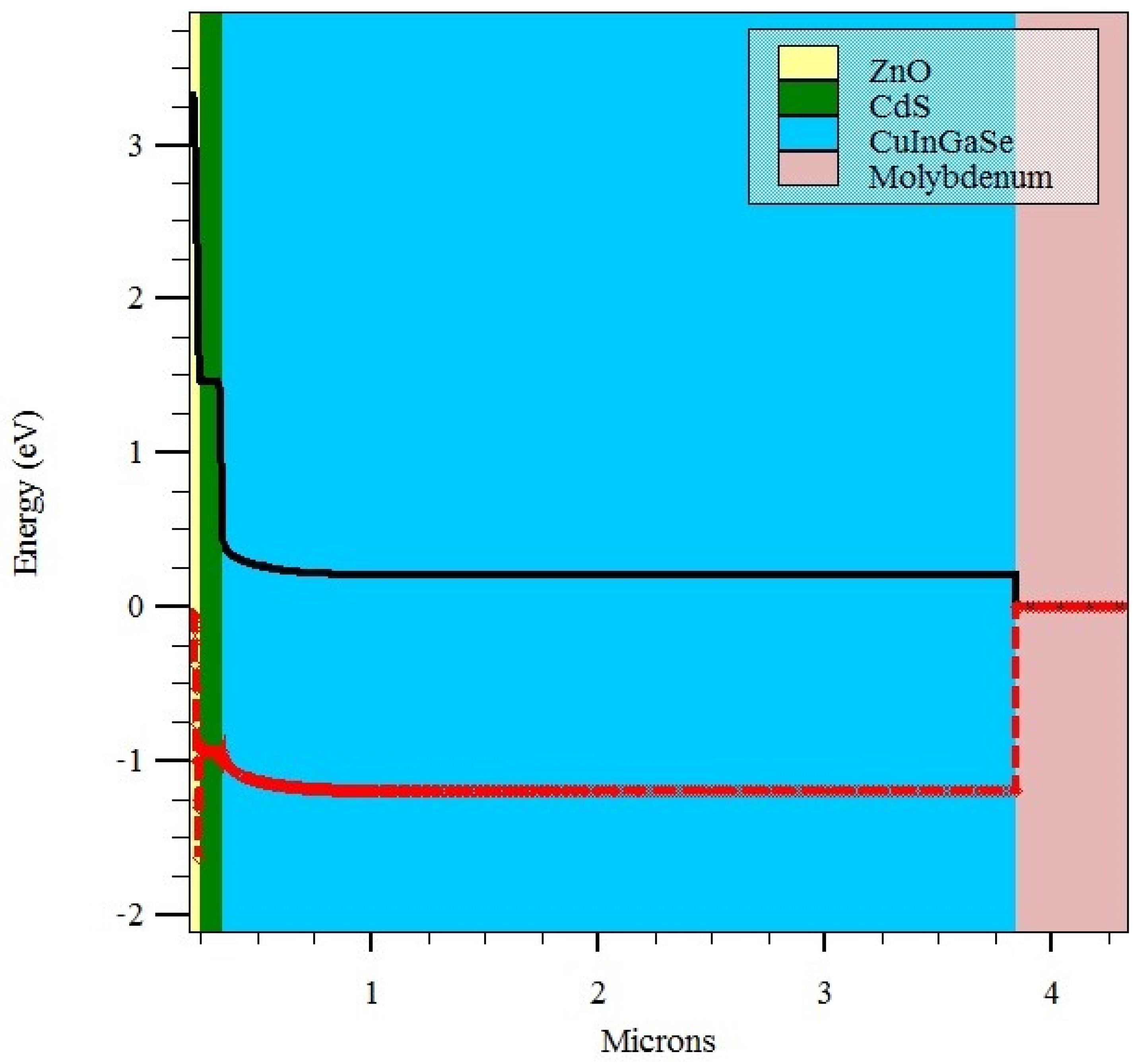
According to the structure of the solar cell shown in Figure 2, the band structure of the bottom cell and the difference in the energy state of different materials in the conduction and valence bands is depicted in Figure 6. The conduction band and valence band curves are shown in black and red, respectively. The smoother the changes between different layers, the better the transfer is due to better alignment of the bands. Due to the fact that the band gap in the bottom cell is larger, the electron accelerates and passes, which causes a break in the Schottky barrier.
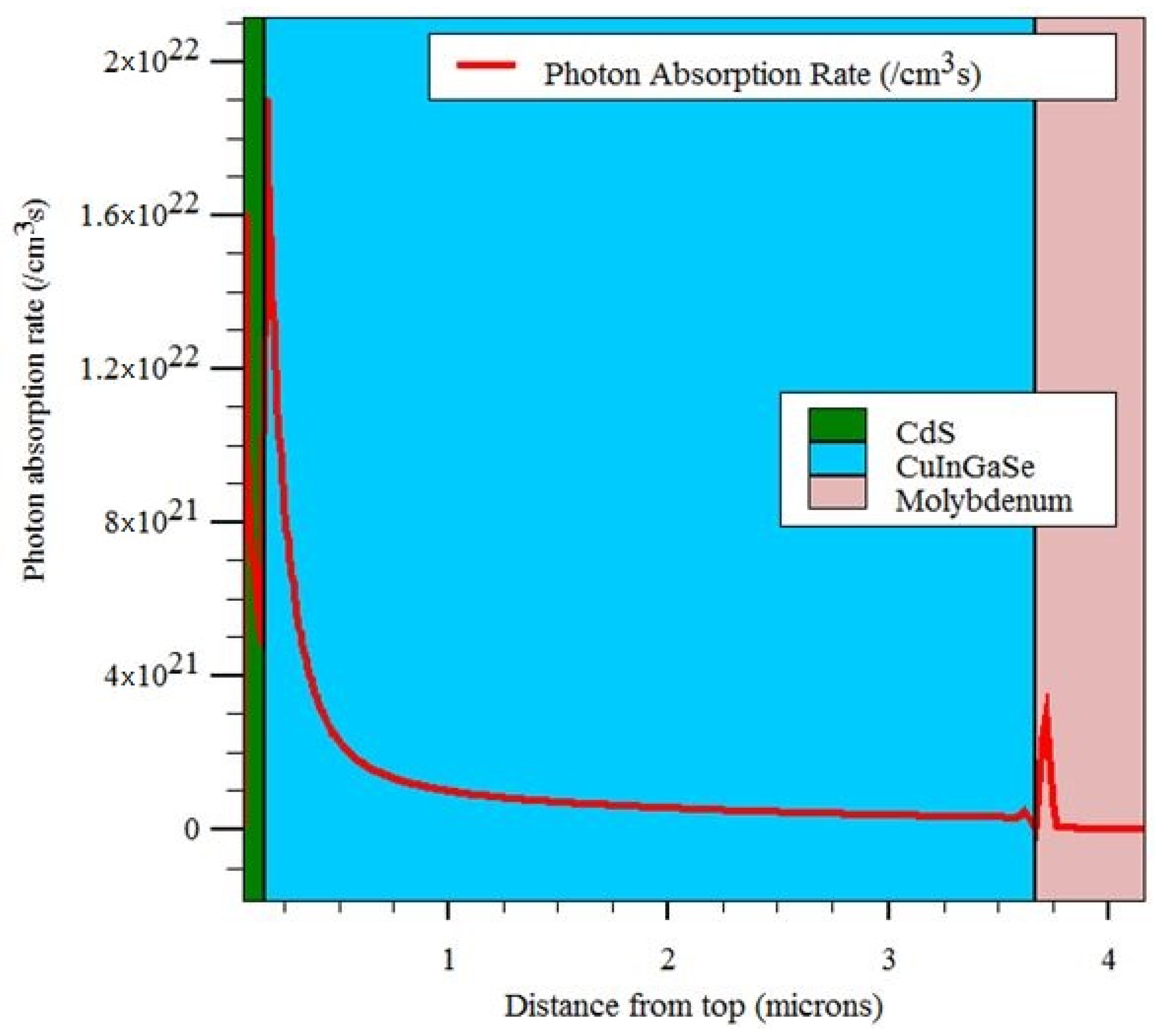
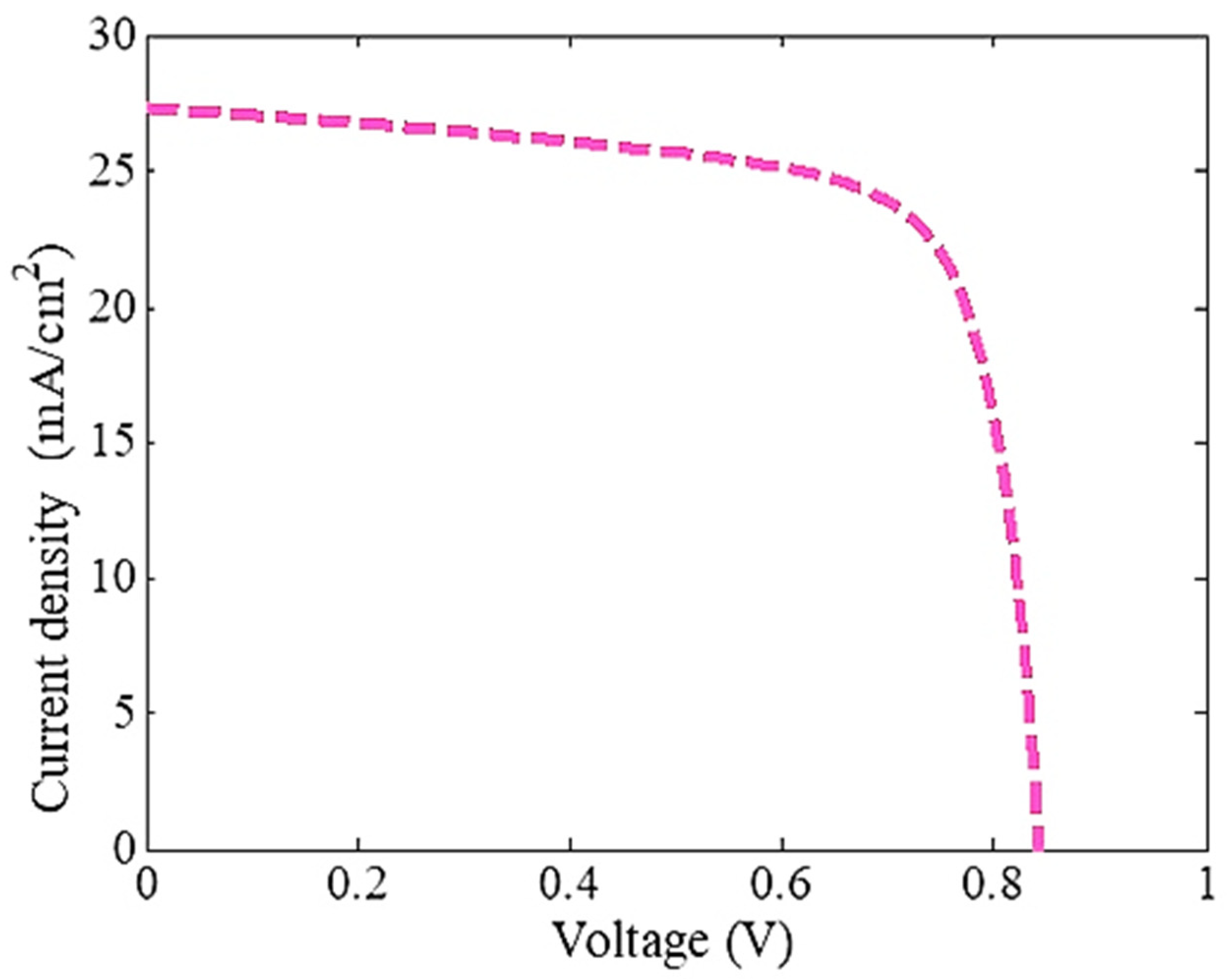
Figure 7 shows the number of photons absorbed per area unit of the solar cell per time unit in terms of wavelength for a single-junction CIGS solar cell. As indicated in Figure 8, the J-V characteristic is used to compare and determine the basic parameters of the solar cell. The values obtained from the simulation of the bottom cell are given in Table 3.
3.3. Perovskite/CIGS Tandem Solar Cell
In this section, we will simulate and fully evaluate the perovskite/CIGS dual-junction solar cell according to the top and bottom cells examined in the previous sections. The pn junction has a smaller discharge area than the pin junction, thus increasing the recombination of carriers and reducing optical losses. In this type of connection, due to the homogeneity of layers p and n, they create a strong internal electric field by which the separation and transfer of carriers are done.
Considering that the effect of different metal grids on perovskite/CIGS dual-junction solar cell has been investigated before [38] and because the most important characteristic of the above electrode is its working function, then in this structure, due to the proximity of Au working function to perovskite, Au as a metal connection is used.
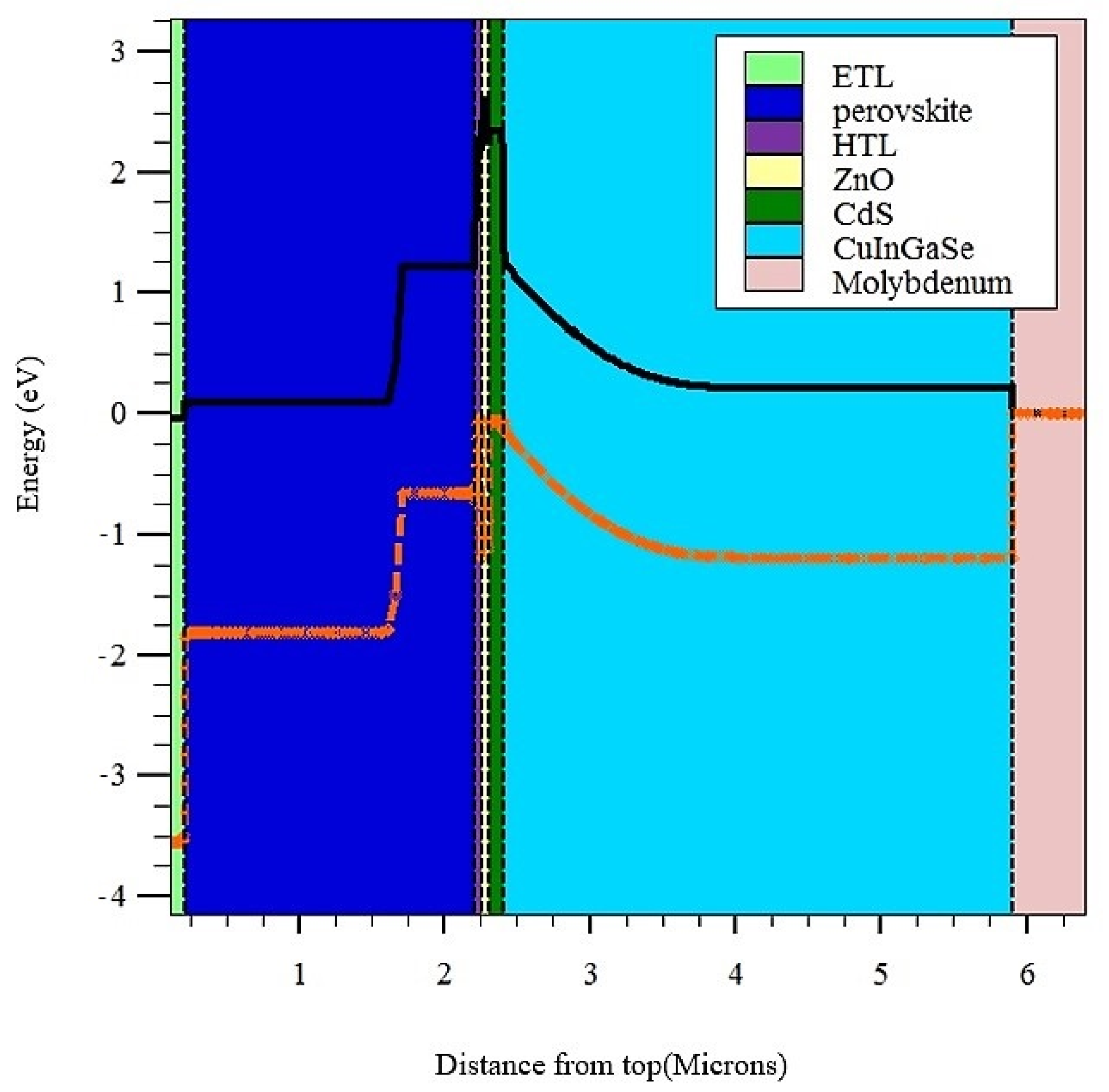
Figure 9 shows the band structure of a dual-junction solar cell. In this figure, the conduction band is marked in black, and the valence band is marked in red. The energy band diagram (EBD) is to examine the overall performance of carriers in the solar cell. According to the results obtained in the previous sections, the value of the top cell is higher (1.14 V), which is also confirmed by the EBD diagram. It is observed that in the intersection, the edge of the conduction strip and the capacity of a bend are found upwards. This facilitates the movement of the carriers and separates the carriers better in the intersection; thus, it leads to an increase in efficiency.
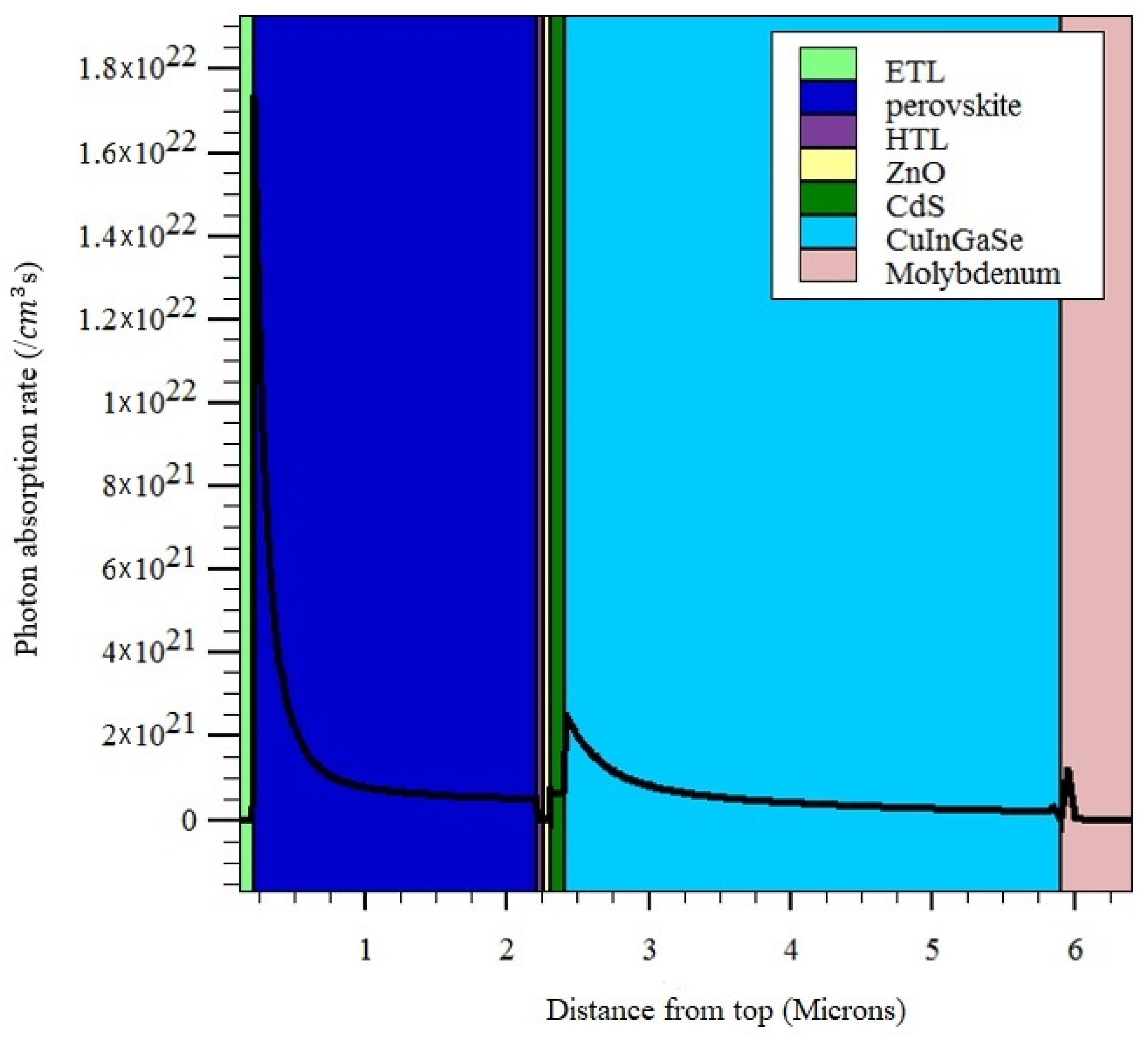
In the next step, we will have a look at the photon absorption rate in a dual-junction solar cell. According to Figure 10, in the perovskite layer, the range of which is determined by the figure guide, we have the highest absorption rate compared to other layers, and in the intersection, the increase in absorption is also observed.
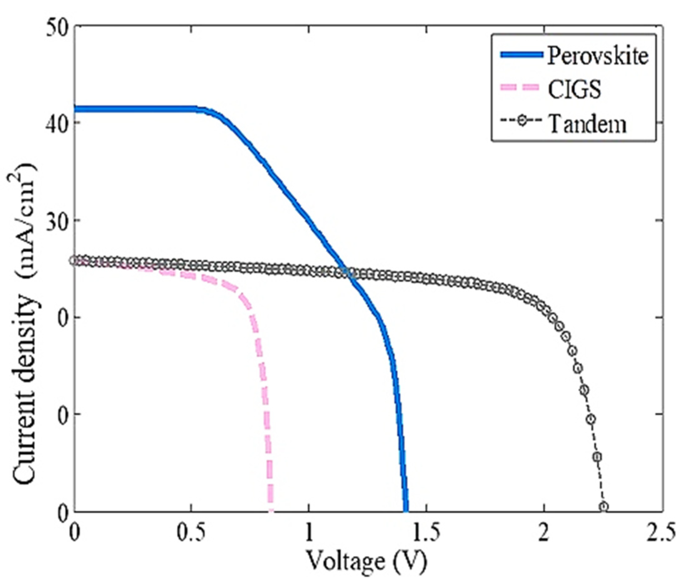
The J-V curve for the tandem solar cell is shown in Figure 11. As demonstrated in the figure, the top cell has a relatively high due to the higher bandgap of the perovskite absorber layer in comparison to the bottom cell. Finally, by comparing the three simulated modes, it will be represented that in the tandem mode, the highest amount of voltage is obtained compared to the two single-junction modes.
The photovoltaic parameters obtained from the perovskite/CIGS dual-junction solar cell simulation are given in Table 4 and are also compared with the single-junction cells of perovskite and CIGS. Similar work is also shown in the comparison table. The amount of short-circuit currents obtained in the top cell with respect to the homojunction p-n perovskite solar cells is reasonable [39,40,41,42,43,44].
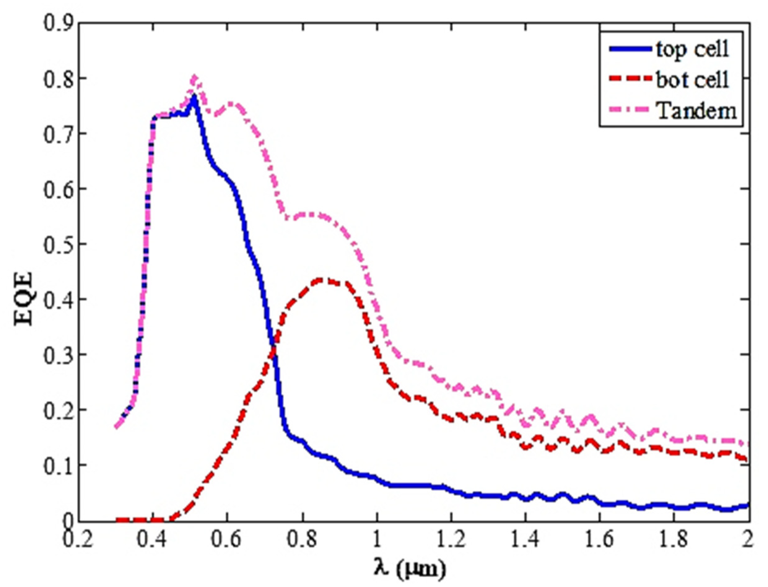
According to Table 4, we encountered an increase in in dual-junction mode, which has also increased efficiency. Figure 11 illustrates the external quantum efficiency (EQE) in terms of the wavelength of the incoming light for different top and bottom cell values. The results obtained in Figure 12 show that the highest EQE of 80% and 79% are between wavelengths of 0.4 μm and 0.9 μm for the perovskite and CIGS solar cells, respectively. Due to the refractive index of perovskite and CIGS, oscillations occur in the wavelength range of more than 1000 nm [45].
Given that the idea of this paper is to connect the perovskite p-n homojunction in a dual-junction structure, it is noteworthy to consider the possibility of constructing such a structure, which was made in 2019 [26]. To further confirm this connection, KPFM measurements were performed on the cross section of the homojunction structure in the dark. The efficiency of homojunction perovskite cells has been confirmed at 20.5% by the National Institute of Metrology in China. In order to evaluate the stability of homojunction, transmission electron microscopy (TEM) studies were performed that stored homojunction perovskites in ambient air in the dark for 160 hours. The stability of homojunction has increased by about 3% compared to heterojunction, and they are relatively stable against moisture and oxygen [26].
4. Conclusions
The report first simulated the perovskite single-junction solar cell, which is a p-n diode connection, n- or p-type doping is performed by stoichiometric control of perovskite precursors, with a cell efficiency of 21.65%. The CIGS single-junction solar cell is then simulated with a 1.4 eV band gap, with an efficiency of 11.46%. The photovoltaic parameters, photon absorption diagram, energy band structure, and J-V are each analyzed separately. Most perovskite structures are in the form of p-i-n connections, but in this structure, n-type and p-type homojunction perovskite connections are used. The task of transferring and separating the carriers is the responsibility of the internal electric field. Carrier light losses are reduced, which leads to increased absorption and efficiency of the solar cell. Finally, the perovskite cell was simulated and examined as a top cell with a 1.9 eV band gap and a CIGS cell as a bottom cell with a 4-terminal architecture as a dual-junction. In the dual-junction state, the of the cell 25.80, the was 2.25 V, the fill factor was 73.02%, and the efficiency was 30.71%. Comparing the perovskite p-n junction with the p-i-n junction and the experimental work is in the next step of our research.
Author Contributions
M.H. designed and performed simulations and analyzed data; S.O. supervised, edited, and prepared the final draft of the manuscript. All authors have read and agreed to the published version of the manuscript.
Funding
This research received no external funding.
Institutional Review Board Statement
Not applicable.
Informed Consent Statement
Not applicable.
Data Availability Statement
Not applicable.
Acknowledgments
This work has been done in Nano-photonics and Optoelectronics Research Laboratory (NORLab), Shahid Rajaee University.
Conflicts of Interest
The authors declare that they have no known competing financial interests or personal relationships that could have appeared to influence the work reported in this paper.
Appendix A
The general process of performing optical and electrical simulations is shown in Figure A1.
Figure A1.
The flowchart of general process of performing optical and electrical simulations.

References
- Kojima, A.; Teshima, K.; Shirai, Y.; Miyasaka, T. Organometal Halide Perovskites as Visible-Light Sensitizers for Photovoltaic Cells. J. Am. Chem. Soc. 2009, 131, 6050–6051. [Google Scholar] [CrossRef] [PubMed]
- Trinh, X.-L.; Kim, H.-C. Fully solution-processed perovskite solar cells fabricated by lamination process with silver nanoparticle film as top electrode. Energy Rep. 2020, 6, 1297–1303. [Google Scholar] [CrossRef]
- Yousaf, S.A.; Imran, M.; Ikram, M.; Ali, S. The critical role of metal oxide electron transport layer for perovskite solar cell. Appl. Nanosci. 2018, 8, 1515–1522. [Google Scholar] [CrossRef]
- Green, M.A.; Ho-Baillie, A.; Snaith, H.J. The emergence of perovskite solar cells. Nat. Photonics 2014, 8, 506–514. [Google Scholar] [CrossRef]
- Yang, Z.; Shang, A.; Qin, L.; Zhan, Y.; Zhang, C.; Gao, P.; Ye, J.; Li, X. Broadband and wide-angle light harvesting by ultra-thin silicon solar cells with partially embedded dielectric spheres. Opt. Lett. 2016, 41, 1329–1332. [Google Scholar] [CrossRef]
- Xu, Z.; Qiao, H.; Huangfu, H.; Li, X.; Guo, J.; Wang, H. Optical absorption of several nanostructures arrays for silicon solar cells. Opt. Commun. 2015, 356, 526–529. [Google Scholar] [CrossRef]
- Bou, A.; Ghahremanirad, E.; Olyaee, S.; Bisquert, J. Inductive Loop in the Impedance Response of Perovskite Solar Cells Explained by Surface Polarization Model. J. Phys. Chem. Lett. 2018, 8, 1402–1406. [Google Scholar]
- Zhang, Y.; Zhai, G.; Gao, L.; Ren, J.; Yu, J.; Yang, Y.; Ha, Y.; Liu, X.; Xu, B.; Wu, Y. Improving performance of perovskite solar cells based on ZnO nanorods via rod-length control and sulfidation treatment. Mater. Sci. Semicond. Process. 2020, 117, 105205. [Google Scholar] [CrossRef]
- Ghahremanirad, E.; Olyaee, S.; Nejand, B.A.; Nazari, P.; Ahmadi, V.; Abedi, K. Improving the performance of perovskite solar cells using kesterite mesostructure and plasmonic network. Sol. Energy 2018, 169, 498–504. [Google Scholar] [CrossRef]
- Lin, L.; Jiang, L.; Li, P.; Fan, B.; Qiu, Y.; Yan, F. Simulation of optimum band structure of HTM-free perovskite solar cells based on ZnO electron transporting layer. Mater. Sci. Semicond. Process. 2018, 90, 1–6. [Google Scholar] [CrossRef]
- Ghahremanirad, E.; Olyaee, S.; Nejand, B.A.; Ahmadi, V.; Abedi, K. Hexagonal Array of Mesoscopic HTM-Based Perovskite Solar Cell with Embedded Plasmonic Nanoparticles. Phys. Status Solidi 2017, 255, 1700291. [Google Scholar] [CrossRef]
- Li, G.; Wang, Y.; Huang, L.; Zeng, R.; Sun, W. Inhibited Aggregation of Lithium Salt in Spiro-OMeTAD for Perovskite Solar Cells. Crystals 2022, 12, 290. [Google Scholar] [CrossRef]
- Ruth, A.; Holland, M.; Rockett, A.; Sanehira, E.; Irwin, M.D.; Steirer, K.X. Charge Compensation by Iodine Covalent Bonding in Lead Iodide Perovskite Materials. Crystals 2022, 12, 88. [Google Scholar] [CrossRef]
- Wang, W. Fabrication of CuInGaSe2 Thin Film Solar Cells using Low-Cost Air-Stable Inks. Ph.D. Thesis, Oregon State University, Corvallis, OR, USA, 2012. [Google Scholar]
- Chandrasekaran, V. Effect of Heat Treatments and Reduced Absorber Layer Thickness on Cu (In, Ga) Se2 Thin Film Solar Cells. Master’s Thesis, University of South Florida, Tampa, FL, USA, 2005. [Google Scholar]
- Al Naser, Q.A.H.; Hilou, H.; Abdulkader, A.F. The Last Development in III-V Multi-Junction Solar Cells. In Proceedings of the 2009 ISECS International Colloquium on Computing, Communication, Control, and Management, Sanya, China, 8–9 August 2009; pp. 373–378. [Google Scholar]
- Jianmin, H.; Yiyong, W.; Jingdong, X.; Dezhuang, Y.; Zhongwei, Z. Degradation behaviors of electrical properties of GaInP/GaAs/Ge solar cells under <200keV proton irradiation. Sol. Energy Mater. Sol. Cells 2008, 92, 1652–1656. [Google Scholar] [CrossRef]
- Takamoto, T.; Kaneiwa, M.; Imaizumi, M.; Yamaguchi, M. InGaP/GaAs-based multijunction solar cells. Prog. Photovolt. Res. Appl. 2005, 13, 495–511. [Google Scholar] [CrossRef]
- Sengar, B.S.; Garg, V.; Kumar, A.; Dwivedi, P. Numerical Simulation: Design of High-Efficiency Planar p-n Homojunction Perovskite Solar Cells. IEEE Trans. Electron Devices 2021, 68, 2360–2364. [Google Scholar] [CrossRef]
- Ghahremanirad, E.; Olyaee, S.; Hedayati, A.M. The Influence of Embedded Plasmonic Nanostructures on the Optical Absorption of Perovskite Solar Cells. Photonics 2019, 6, 37. [Google Scholar] [CrossRef] [Green Version]
- Fang, Z.; Zeng, Q.; Zuo, C.; Zhang, L.; Xiao, H.; Cheng, M.; Hao, F.; Bao, Q.; Yuan, Y.; Wu, W.-Q.; et al. Perovskite-based tandem solar cells. Sci. Bull. 2020, 66, 621–636. [Google Scholar] [CrossRef]
- Liu, L.; Xiao, Z.; Zuo, C.; Ding, L. Inorganic perovskite/organic tandem solar cells with efficiency over 20%. J. Semicond. 2021, 42, 020501. [Google Scholar] [CrossRef]
- Hedayati, M.; Olyaee, S.; Ghorashi, S.M.B. The Effect of Adsorbent Layer Thickness and Gallium Concentration on the Efficiency of a Dual-Junction Copper Indium Gallium Diselenide Solar Cell. J. Electron. Mater. 2019, 49, 1454–1461. [Google Scholar] [CrossRef]
- Gharibzadeh, S.; Hossain, I.M.; Fassl, P.; Nejand, B.A.; Abzieher, T.; Schultes, M.; Ahlswede, E.; Jackson, P.; Powalla, M.; Paetzold, U.W.; et al. 2D/3D heterostructure for semitransparent perovskite solar cells with engineered bandgap enables efficiencies exceeding 25% in four-terminal tandems with silicon and CIGS. Adv. Funct. Mater. 2020, 30, 1909919. [Google Scholar] [CrossRef] [Green Version]
- Madan, J.; Shivani; Pandey, R.; Sharma, R. Device simulation of 17.3% efficient lead-free all-perovskite tandem solar cell. Sol. Energy 2020, 197, 212–221. [Google Scholar] [CrossRef]
- Cui, P.; Wei, D.; Ji, J.; Huang, H.; Jia, E.; Dou, S.; Wangm, T.; Wang, W.; Li, M. Planar p–n homojunction perovskite solar cells with efficiency exceeding 21.3%. Nat. Energy 2019, 4, 150–159. [Google Scholar] [CrossRef]
- Wang, Q.; Shao, Y.; Xie, H.; Lyu, L.; Liu, X.; Gao, Y.; Huang, J. Qualifying composition dependent p and n self-doping in CH3NH3PbI3. Appl. Phys. Lett. 2014, 105, 163508. [Google Scholar] [CrossRef] [Green Version]
- Islam, A.; Matin, M.; Aliyu, M.M.; Sulaiman, Y.; Amin, N. A Numerical Analysis on CdS: O Window Layer for Higher Efficiency Cdte Solar Cells. In Proceedings of the 2009 1st International Conference on the Developements in Renewable Energy Technology (ICDRET), Dhaka, Bangladesh, 17–19 December 2009; IEEE: Piscataway, NJ, USA; pp. 1–4. [Google Scholar]
- Sze, S.M. Semiconductor Devices: Physics and Technology; John Wiley & Sons: Hoboken, NJ, USA, 2008. [Google Scholar]
- Sutherland, J.E.; Hauser, J.R. A computer analysis of heterojunction and graded composition solar cells. IEEE Trans. Electron Devices 1977, 24, 363–372. [Google Scholar] [CrossRef]
- Sze, S.M.; Ng, K.K. Physics of Semiconductor Devices; John Wiley & Sons: Hoboken, NJ, USA, 2006. [Google Scholar]
- Entner, R. Modeling and Simulation of Negative Bias Temperature Instability; Technische Universitat Wien: Judendorf-Straßengel, Austria, 2007. [Google Scholar]
- Shockley, W.; Queisser, H.J. Detailed balance limit of efficiency of p-n junction solar cells. J. Appl. Phys. 1961, 32, 510–519. [Google Scholar] [CrossRef]
- Lundstrom, M.; Schuelke, R. Numerical analysis of heterostructure semiconductor devices. IEEE Trans. Electron Devices 1983, 30, 1151–1159. [Google Scholar] [CrossRef]
- Elbar, M.; Tobbeche, S.; Merazga, A. Effect of top-cell CGS thickness on the performance of CGS/CIGS tandem solar cell. Sol. Energy 2015, 122, 104–112. [Google Scholar] [CrossRef]
- Karimi, E.; Ghorashi, S.M.B. Simulation of perovskite solar cell with P3HT hole-transporting materials. J. Nanophotonics 2017, 11, 032510. [Google Scholar] [CrossRef]
- Fotis, K. Modeling and Simulation of a Dual-Junction CIGS Solar Cell using Silvaco ATLAS; Naval Postgraduate School: Monterey, CA, USA, 2012. [Google Scholar]
- Hedayati, M.; Olyaee, S. Proposal of CIGS dual-junction solar cell and investigation of different metal grids effect. Opt. Quantum Electron. 2020, 52, 347. [Google Scholar] [CrossRef]
- Fu, F.; Pisoni, S.; Weiss, T.P.; Feurer, T.; Wäckerlin, A.; Fuchs, P.; Nishiwaki, S.; Zortea, L.; Tiwari, A.N.; Buecheler, S. Compositionally Graded Absorber for Efficient and Stable Near-Infrared-Transparent Perovskite Solar Cells. Adv. Sci. 2018, 5, 1700675. [Google Scholar] [CrossRef] [PubMed] [Green Version]
- Su, J.; Yang, H.; Xu, Y.; Tang, Y.; Yi, Z.; Zheng, F.; Zhao, F.; Liu, L.; Wu, P.; Li, H. Based on Ultrathin PEDOT:PSS/c-Ge Solar Cells Design and Their Photoelectric Performance. Coatings 2021, 11, 748. [Google Scholar] [CrossRef]
- Balaji, P.; Dauksher, W.J.; Bowden, S.G.; Augusto, A. Flexible Silicon Heterojunction Solar Cells on 40 µm Thin Substrates. In Proceedings of the 2019 IEEE 46th Photovoltaic Specialists Conference (PVSC), Chicago, IL, USA, 16–21 June 2019; IEEE: Piscataway, NJ, USA; pp. 1089–1092. [Google Scholar]
- Bashiri, H.; Karami, M.M.A.; Nejad, S.M. Crystalline silicon solar cell engineering to improve fill factor, open circuit voltage, short circuit current and overall cell efficiency. Modares J. Electr. Eng. 2015, 14, 6–14. [Google Scholar]
- Kim, S.; Dao, V.A.; Shin, C.; Balaji, N.; Yi, J. Influence of n-doped μc-Si: H back surface field layer with micro growth in crystalline-amorphous silicon heterojunction solar cells. J. Nanosci. Nnanotechnol. 2014, 14, 9258–9262. [Google Scholar] [CrossRef] [PubMed]
- Meroni, S.M.P.; Hooper, K.E.A.; Dunlop, T.; Baker, J.A.; Worsley, D.; Charbonneau, C.; Watson, T.M. Scribing Method for Carbon Perovskite Solar Modules. Energies 2020, 13, 1589. [Google Scholar] [CrossRef] [Green Version]
- Zhao, D.; Huang, J.; Qin, R.; Yang, G.; Yu, J. Efficient Visible-Near-Infrared Hybrid Perovskite:PbS Quantum Dot Photodetectors Fabricated Using an Antisolvent Additive Solution Process. Adv. Opt. Mater. 2018, 6, 1800979. [Google Scholar] [CrossRef]
Figure 1.
Carrier generation and transport in heterojunction and homojunction perovskite solar cells. Black and red arrows indicate the direction of the internal electric field and the direction of transmission of the carriers, respectively. Electrons are shown with pink circles and holes with yellow circles.

Figure 2.
Schematic diagram of (a) single-junction top solar cell, (b) single-junction bottom solar cell, and (c) perovskite/CIGS dual-junction solar cell with 4-terminal architecture simulated in this report.
Figure 2.
Schematic diagram of (a) single-junction top solar cell, (b) single-junction bottom solar cell, and (c) perovskite/CIGS dual-junction solar cell with 4-terminal architecture simulated in this report.

Figure 3.
Energy band diagram of perovskite solar cell (Top Cell).

Figure 4.
The J-V characteristics in the perovskite top cell.

Figure 5.
The photon absorption rate curve in top solar cell (perovskite).

Figure 6.
The energy band diagram of CIGS solar cell (bottom cell).

Figure 7.
The photon absorption rate curve for bottom cell (CIGS).

Figure 8.
The J-V curve characteristics for the CIGS bottom cell.

Figure 9.
The energy band diagram of tandem solar cell.

Figure 10.
The absorption rate curve for perovskite/CIGS tandem solar cell.

Figure 11.
Comparison of J-V characteristics for the top, bottom, and tandem solar cell.

Figure 12.
The effect of EQE on top (perovskite) and bottom (CIGS) solar cells.


Table 1.
Semiconductor parameters used for simulation.
| Parameters | Symbol | Unit | Perovskite | HTL | ETL | CdS | CIGS |
|---|---|---|---|---|---|---|---|
| Band gap [35] | eV | 1.9 | 2.31 | 3.5 | 2.4 | 1.4 | |
| Electron affinity [36] | 3.9 | 4.08 | 3.9 | 4 | 4.6 | ||
| Relative permittivity [35] | F.cm−1 | 6.5 | 9 | 6.5 | 10 | 13.6 | |
| Electron mobility [35] | cm2/V.s | 1.6 | 25 | 1.6 | 100 | 100 | |
| Hole mobility [35] | cm2/V.s | 0.2 | 100 | 0.2 | 25 | 25 | |
| Conduction band effective density of states [35] | 2.2 × 10¹⁸ | 2.2 × 10¹⁸ | 2.2 × 10¹⁸ | 2.2 × 10¹⁸ | 2.2 × 10¹⁸ | ||
| Valence band effective density of states [35] | 1.8 × 10¹⁹ | 1.8 × 10¹⁹ | 1.8 × 10¹⁹ | 1.8 × 10¹⁹ | 1.8 × 10¹⁹ |
Table 2.
Simulated results for top solar cell.
| Perovskite top cell | 41.45 | 1.41 | 51.06 | 21.65 |
Table 3.
Simulated results for bottom solar cell.
| CIGS bottom cell | 25.80 | 0.84 | 72.93 | 11.46 |
Publisher’s Note: MDPI stays neutral with regard to jurisdictional claims in published maps and institutional affiliations. |
© 2022 by the authors. Licensee MDPI, Basel, Switzerland. This article is an open access article distributed under the terms and conditions of the Creative Commons Attribution (CC BY) license (https://creativecommons.org/licenses/by/4.0/).
Share and Cite
MDPI and ACS Style
Hedayati, M.; Olyaee, S. High-Efficiency p-n Homojunction Perovskite and CIGS Tandem Solar Cell. Crystals 2022, 12, 703. https://0-doi-org.brum.beds.ac.uk/10.3390/cryst12050703
AMA Style
Hedayati M, Olyaee S. High-Efficiency p-n Homojunction Perovskite and CIGS Tandem Solar Cell. Crystals. 2022; 12(5):703. https://0-doi-org.brum.beds.ac.uk/10.3390/cryst12050703
Chicago/Turabian StyleHedayati, Maryam, and Saeed Olyaee. 2022. "High-Efficiency p-n Homojunction Perovskite and CIGS Tandem Solar Cell" Crystals 12, no. 5: 703. https://0-doi-org.brum.beds.ac.uk/10.3390/cryst12050703
Note that from the first issue of 2016, this journal uses article numbers instead of page numbers. See further details here.