Article

Study of PDMS Microchannels for Liquid Crystalline Optofluidic Devices in Waveguiding Photonic Systems

1
Faculty of Physics, Warsaw University of Technology, 00-662 Warsaw, Poland
2
Faculty of Chemistry, Warsaw University of Technology, 00-664 Warsaw, Poland
3
Centre for Advanced Materials and Technologies (CEZAMAT), Warsaw University of Technology, 02-822 Warsaw, Poland
*
Author to whom correspondence should be addressed.
Submission received: 21 April 2022 / Revised: 11 May 2022 / Accepted: 17 May 2022 / Published: 19 May 2022
(This article belongs to the Special Issue Optical and Molecular Aspects of Liquid Crystals)

Abstract

:
Microchannels in LC:PDMS structures must be of good quality and suitable geometry to achieve the desired orientation of the liquid crystalline molecules inside. When applying a casting technique, with the molds obtained even by the most accurate method, i.e., photolithography, it is still crucial to inspect the cross-section of the structure and the surface roughness of the PDMS material. This paper presents a study of PDMS microchannels using a Scanning Electron Microscope (SEM) to make such a characterization as accurate as possible. By comparing images of the samples taken using standard polarized light microscopy and SEM, it is likely to understand the mechanism of the liquid crystal molecular orientation occurring in the samples. The results obtained in this work may be used for numerical simulations and further development of LC:PDMS structures.

1. Introduction

Adaptation of the technologies known from other fields of science in optical applications has become extremely important in recent years. Specifically, the combination of microfluidics used in biotechnology or chemical analysis with the ability to control optical properties has created a new branch of research called optofluidics [1]. Various configurations, including Lab-on-a-Chips (LOCs), microfluidic chips, micro-total-analysis-systems (µ-TASs), or Photonic Lab-on-a-Chips (PhLoCs), allow for more rapid and less expensive research in many areas [2,3,4,5]. One of the basic materials used in microfluidics is polydimethylsiloxane (PDMS) [6]. Due to its parameters such as refractive index of about 1.41 @ 589 nm [7], isotropy, homogeneity, and high optical transparency in the spectral range covering UV, VIS, and NIR [8], PDMS is used in the development of many optofluidic structures, e.g., dye lasers [9] or reconfigurable optical waveguides [10]. Importantly, a mold with sufficient quality and specific geometry is needed to fabricate optofluidic structures in PDMS using a casting technique. There are many methodologies to manufacture molds [11], including 3D printing [12,13,14], micromilling [11,12,15,16], and capillary film processing [17]. In the same context, photolithography is the most widely used for complex and precise structures [18,19].
One of the subjects studied in the area of optofluidics is related to PDMS structures filled with liquid crystals (LCs). The resulting LC:PDMS systems combine the capabilities of microfluidics with extraordinary properties such as anisotropy and birefringence (which are typical for liquid crystalline materials). In particular, cholesteric liquid crystals (CLCs) may be used in PDMS systems to form lasers [20] or biosensing chips [21]. On the other hand, PDMS structures filled with nematics (NLCs) have been, for instance, explored in optofluidic modulators [22], optofluidic grating switches [23], and tunable optofluidic birefringent lenses [24]. Research on LC:PDMS-based optical waveguides also emerged [25,26,27,28,29]. The latter may be potentially applied as reconfigurable optical interconnectors, switches, and wavelength demultiplexers [27,30,31]. It should be emphasized that the performance and operation of LC:PDMS structures are highly dependent on the orientation of the liquid crystal molecules inside. Although orientation layers are typically required in LC-based photonic devices, it has been proven that the rod-like NLC molecules align themselves vertically to the PDMS surface in stationary conditions [32,33]. These stiff boundary conditions within LC:PDMS systems are routinely used in numerical simulations performed using different computational methods [25,26,27,28,34]. However, the overall alignment of NLC molecules in PDMS-embedded microchannels is dependent on their aspect ratio [35]. Moreover, a so-far unexpressed but essential condition for successful fabrication of LC:PDMS structures is the quality of the mold. Because of the ultimate dimensions and high precision requirements for the microchannels acting as the waveguides, the detailed studies of the NLC molecular orientation in PDMS structures fabricated using various molds (i.e., obtained by applying different technologies) have been performed [12,36]. On this basis, it has been concluded that reproducible results with the channels of desired geometry and the NLC molecules aligned perpendicularly to the PDMS surfaces are possible only when the photolithography process is used for molds’ fabrication [36]. In addition, there are many possible methods for bonding the PDMS structures to a substrate [37], which also affects the surface quality [38]. Based on intentional physical and chemical modifications of the PDMS surface [39], it is feasible to make it superhydrophobic, but at the cost of its roughness [40]. In this context, research on the plasma treatment, reducing the PDMS surface roughness [38,41], may be crucial for studying LC:PDMS structures.
This paper shows further investigations on the NLC molecular orientation in PDMS microstructures. Specifically, previously studied microchannels fabricated using a SU-8 photoresist mold [36] are compared with the redesigned structures (of reduced transversal dimensions), also manufactured based on the photolithography process. The main aspects of this work were investigating the orientation of the NLC molecules at PDMS surfaces and analyzing the elastomer surface roughness from the images taken with a Scanning Electron Microscope (SEM). This insight into the fabricated microchannels allows for a more accurate determination of the influence of the PDMS surface quality on the orientation of the NLC molecules and for finding possible sources of defects.

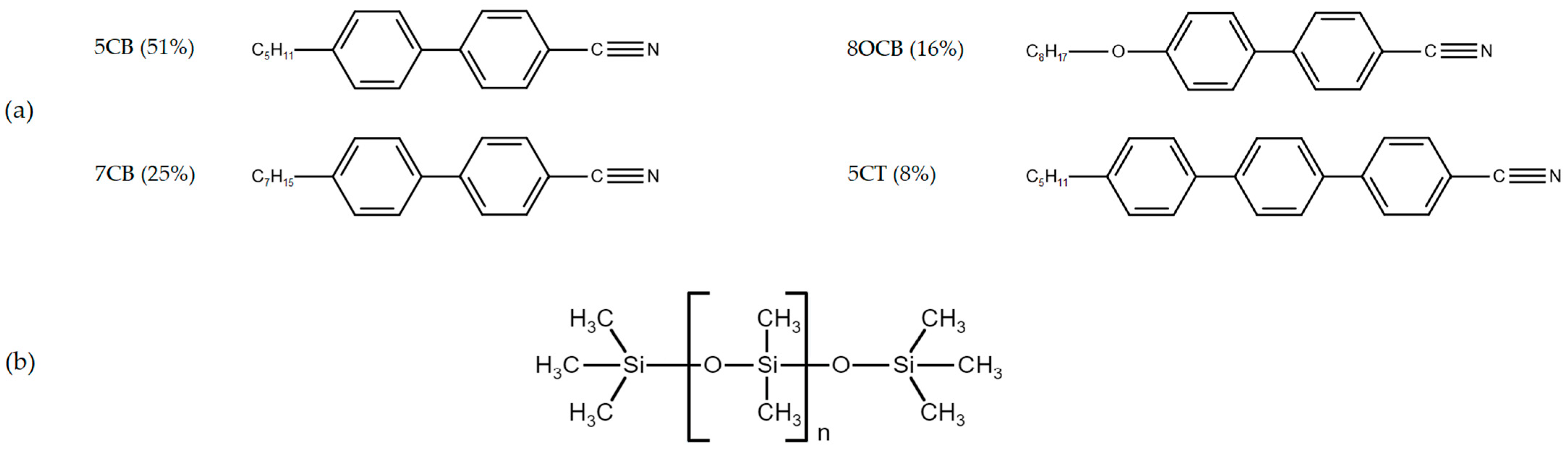
2. Materials and Methods

2.1. Molds Manufacturing

In the current studies, two different molds were used to check the performance of the PDMS structures and compare them with previous samples described in [36]. This approach was decided to optimize the PDMS structures fabricated in the photolithography process and to check the NLC molecular orientation in the microchannels characterized by different aspect ratios. The structures were designed in AutoCAD software (Autodesk, Dublin, Ireland) and then transferred to the chrome masks in the electron-beam lithography process. In this way, two molds were created using different SU-8 photoresists. The nine-step procedure, including silicon substrate preparation, photoresist spin-coating, soft-baking, UV-light illumination, and post-processing, is precisely described in [36]. A SU-8 25 was used in the first case, while the second mold was fabricated using SU-8 2010, with both negative photoresists provided by the Kayaku Advanced Materials Inc. (Westborough, MA, USA) The differences in the photoresists’ characteristics made it necessary to modify some steps in the fabrication process. Specifically, in terms of the parameters that were applied for the second mold, (i) the spin speed in the spin cycle was increased from 1700 to 3000 rpm; (ii) post-exposure baking (PEB) was performed for 210 s at 95 °C (instead of two-step contact hotplate process with PEB time of 60 s at 65 °C and 360 s at 95 °C); (iii) the time of immersing the structure in a dedicated SU-8 developer was reduced from about 180 to 150 s to dissolve unexposed portions of the photoresists. Eventually, after checking by several methods, the height of the structure from the first mold was estimated to be about 30 µm. It was decided to be reduced by applying a SU-8 2010. Following the given steps of the fabrication procedure [36] with suitable modifications described above, a mold with a height of about 12 µm was successfully manufactured. For both molds, no damages or deformations were observed during their fabrication and when manufacturing the PDMS structures, which allowed them to be used repetitively, giving reproducible results.

2.2. LC:PDMS Structures Manufacturing

PDMS material was prepared by mixing the prepolymer (SYLGARD™ 184 Silicone Elastomer Base) with the crosslinker (SYLGARD™ 184 Silicone Curing Agent), both from Dow Corning (Dow Polska, Warsaw, Poland), in a weight ratio of 10:1 [7]. A vacuum pump was used to eliminate air bubbles from PDMS in a liquid form. Then, the prepared mixture was poured onto the mold in a glass container (i.e., a Petri dish), and baked in an oven at a temperature of 75 °C for 90 min. After detaching the cross-linked PDMS from the mold, an elastomer layer with intended microchannels was obtained. A biopsy puncher was used to make inlets and outlets to enable the filling of the channels with liquid crystalline material. The next step in the fabrication process was to bond the PDMS structure to a flat surface (made of a PDMS layer or a glass plate), properly prepared and cleaned. Both elements to be combined were inserted into the chamber with oxygen plasma (Atto Plasma Cleaner, Diener Electronic, Ebhausen, Germany) for 20 s at a reduced pressure of 0.3 mbar. Eventually, the building components of the structure were merged, resulting thus in the target PDMS:PDMS or PDMS:glass samples, respectively, depending on the substrate used.
The nematic liquid crystal (NLC) used for the experimental tests was the E7 LC mixture [42], available from Merck (Darmstadt, Germany). This typical liquid crystalline material was injected into the fabricated PDMS structures using a syringe at room temperature (about 20 °C). The whole volumes of the microchannels were infiltrated using the capillary forces. The transition temperature to the isotropic phase is about 58.3 °C, which is one of the characteristics of the selected LC. Therefore, E7, even in the isotropic state, is not expected to have any impact on the properties of PDMS. The chemical structures of PDMS and the nematic liquid crystal E7 are shown in Figure 1.

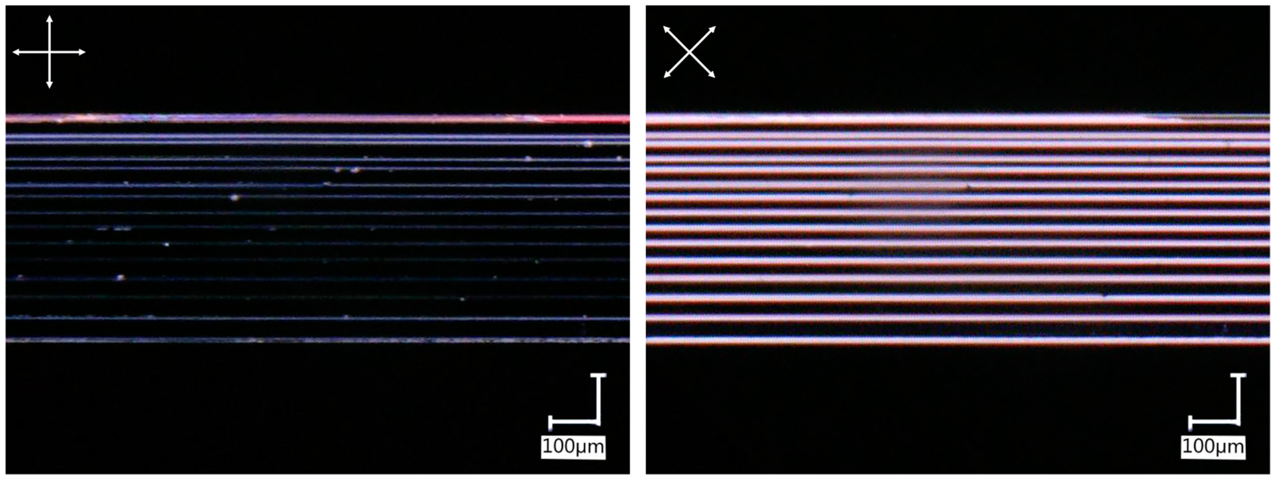
2.3. Optical Measurements and Observations

A digital microscope (KEYENCE VHX-5000, Keyence International, Mechelen, Belgium) equipped with a VH-Z50 long-working-distance zoom lens (50−500×) allowed for the sample’s observations based on the high-resolution images (1600 × 1200 pixels). Specifically, the examined structures placed on the glass stage could be observed in the transmitted and/or reflected light (independently if required). This research used the ability to adapt the mentioned microscope for standard polarizing microscope (POM) measurements. In fact, the main part of the experimental investigations was performed with white light transmitted through the sample located between the crossed polarizers. Additionally, an Olympus LEXT OLS4100 (Olympus Corporation, Tokyo, Japan) microscope was used to acquire preliminary data related to the measurements of the height of the microchannels in PDMS samples. Moreover, a Scanning Electron Microscope (SEM), namely Hitachi SU 8230 (Hitachi Europe Limited, Buckinghamshire, UK), was used to obtain the images of the cross-sections and surfaces of PDMS structures with high magnification. With such advanced equipment, it was possible to examine the samples with the magnification of 25,000× without any problems. However, several steps were taken before observing the samples in the SEM to make this possible. Specifically, the section of the structure to be viewed had to be of appropriate size (with a maximum area of 2 × 2 cm2 and a height up to 2 cm) and sputtered with a layer of Au-Pd (80:20 ratio, thickness < 100 nm).

3. Results

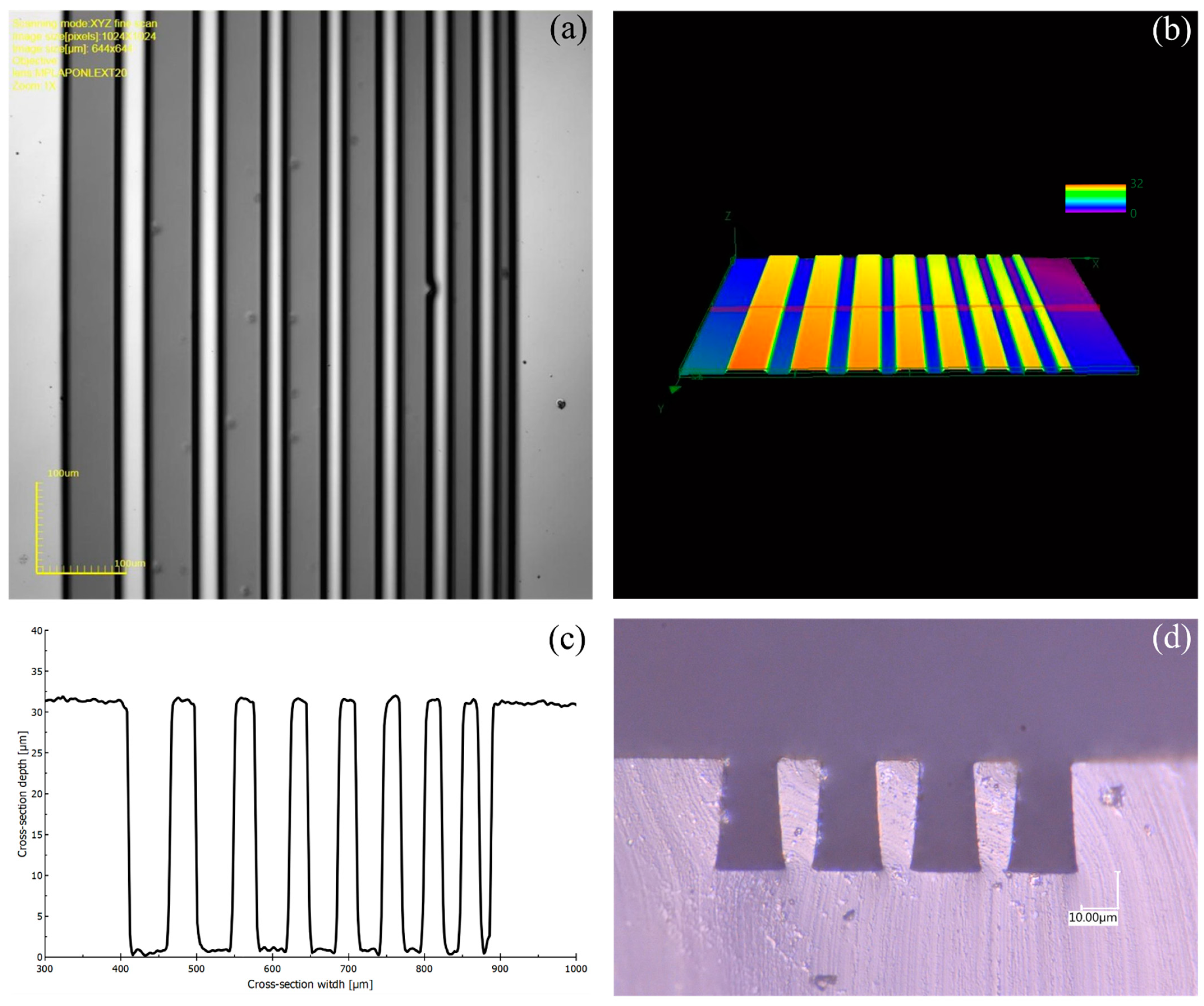
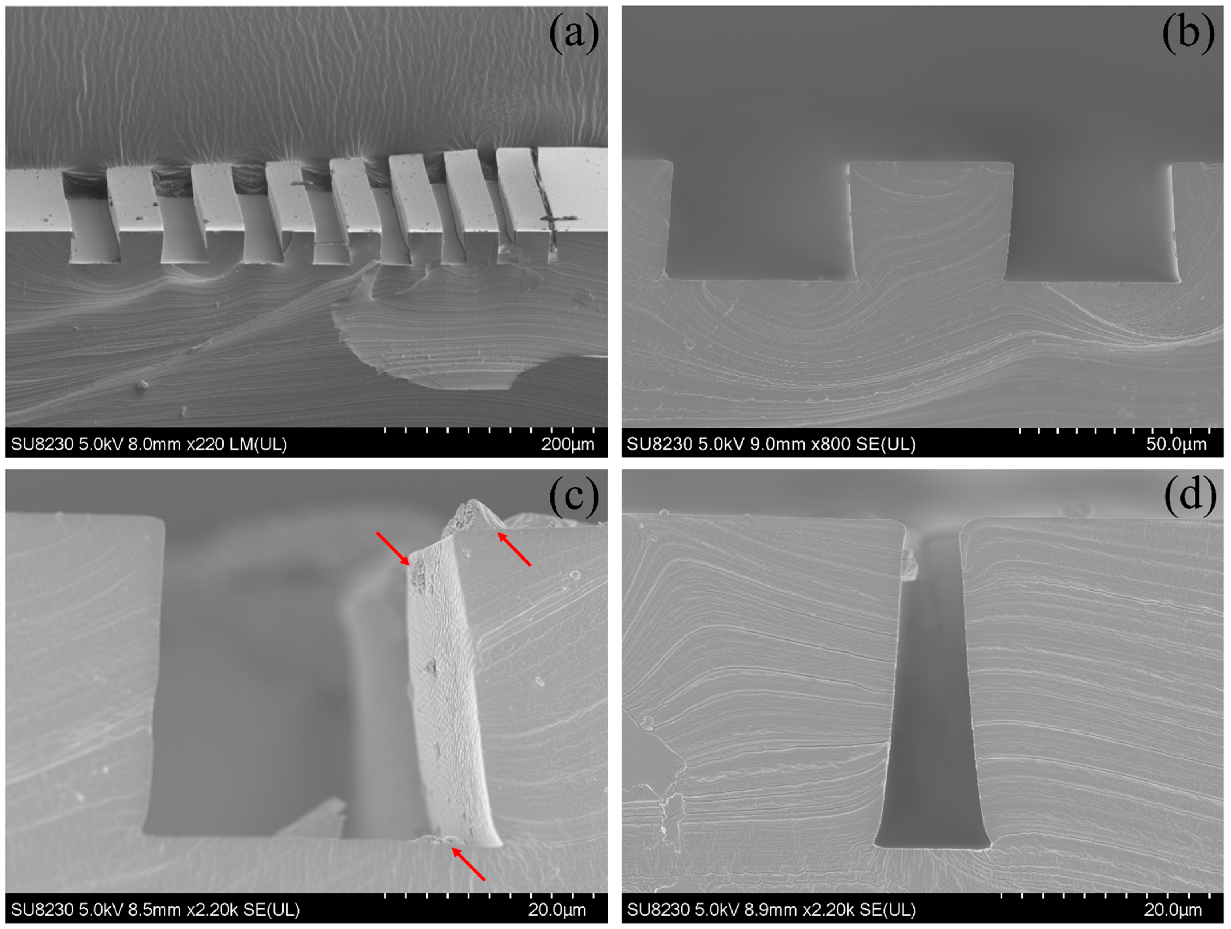
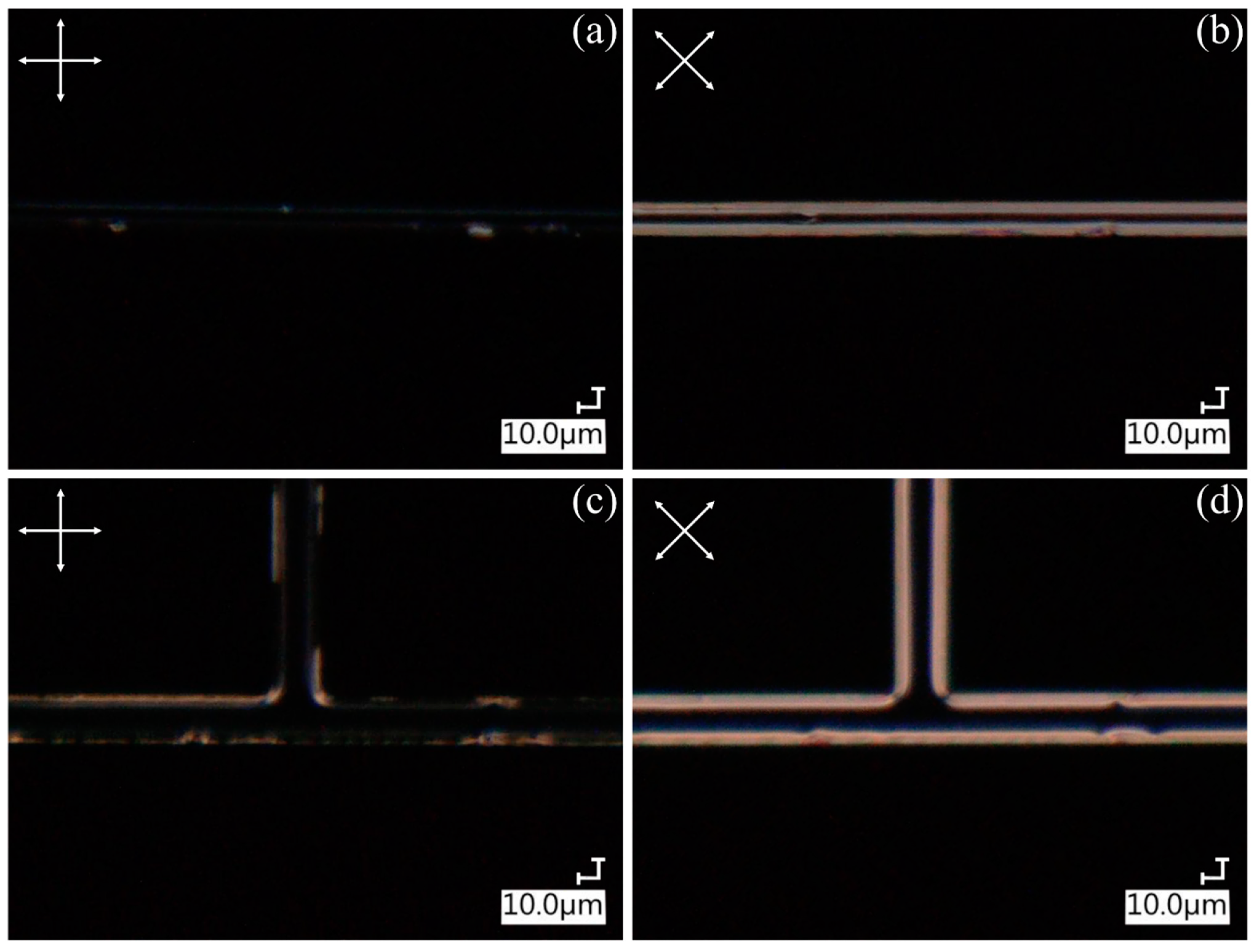
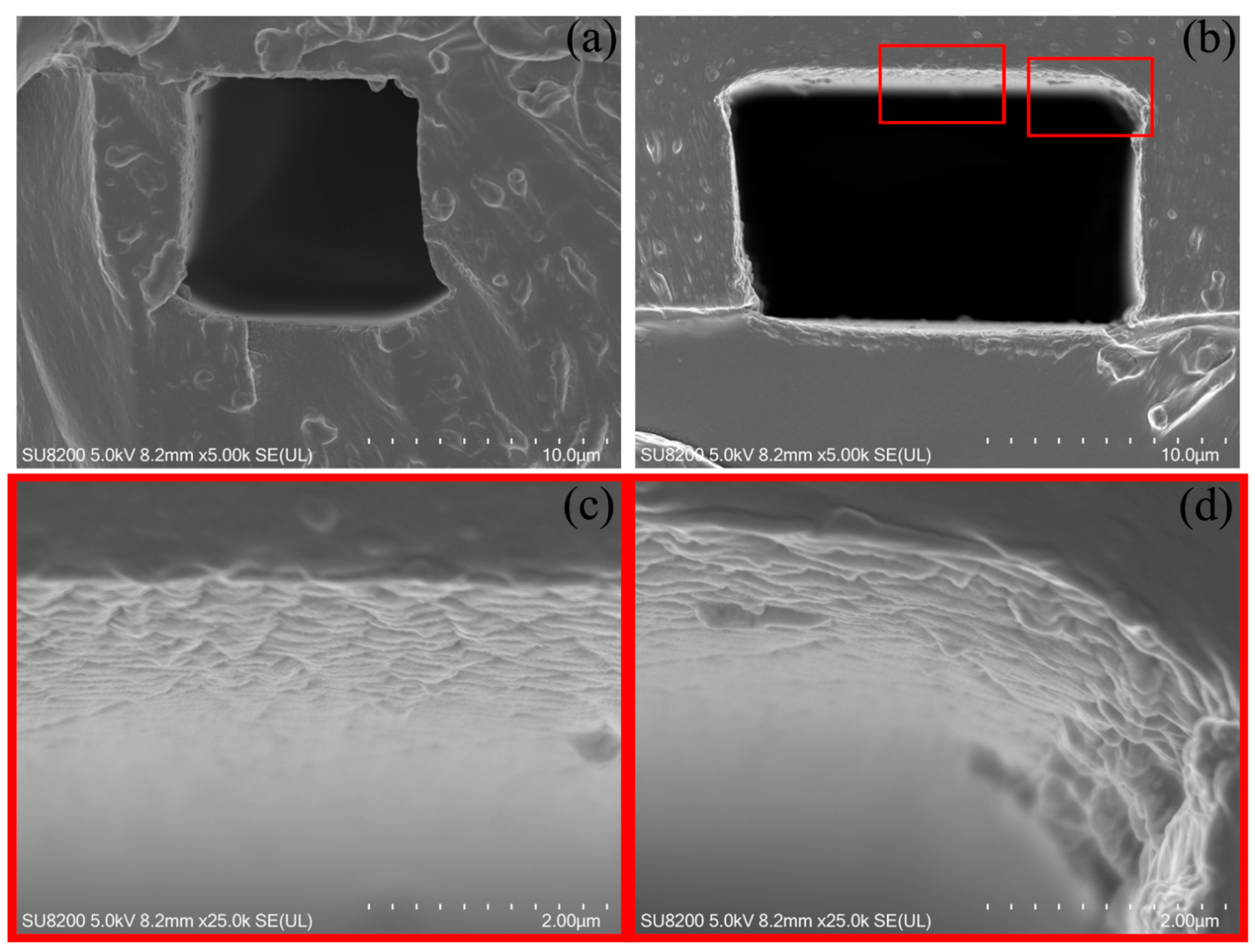
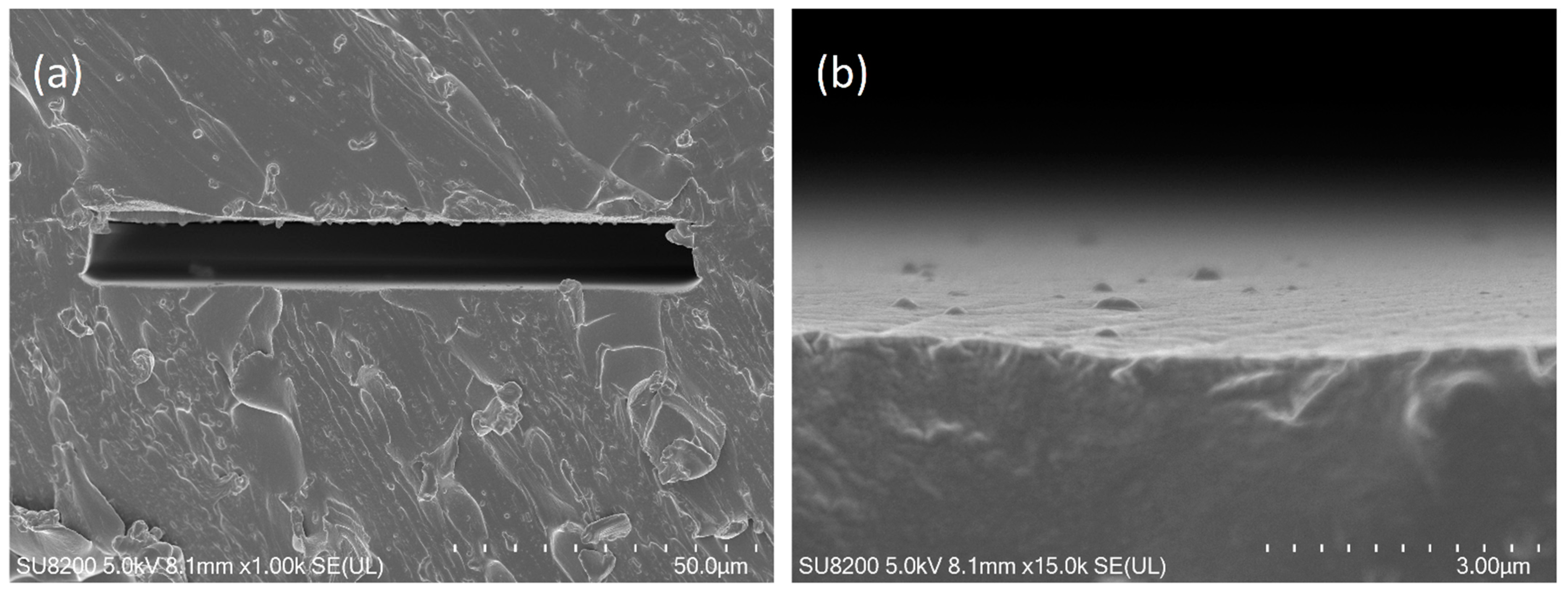
3.1. LC:PDMS Structures with a Height of 30 µm

Based on the results related to the orientation of NLC molecules in PDMS samples reported in our previous work [36], only a limited number of the structures fabricated using a SU-8 mold with a height of about 30 µm are presented in this paper. Specifically, a sample consisting of a series of microchannels with the widths of 10, 20, 25, 30, 35, 40, 45, and 50 µm (Figure 2a,b) was selected to be further compared with the samples obtained from the optimized mold of reduced size (i.e., with a height of 12 µm, see Section 3.2). The channels in the PDMS:glass structure were filled with E7 NLC (with an estimated volumetric flow rate from 3 to 30 nL/min depending on the channel width) and were left to obtain the fixed orientation of the liquid crystalline molecules in the sample. After about 5 min, the NLC molecules were aligned perpendicular to each microchannel wall. From the previously mentioned studies and simulations [25,26,27,28,34], it is clear that the channel’s aspect ratio (height/width, h/w) strongly influences the orientation of the LC molecules. This fact was also confirmed by our previous observations [36], as well as by the results of current studies. In principle, for the channels with a width smaller than a height (i.e., with the aspect ratio h/w > 1), the resulting orientation of the molecules within the whole volume of the channel is strongly dependent on the forces that orient the molecules perpendicular to the sidewalls. It may be proven that for the channels with an aspect ratio greater than 1, molecules across the width of the channel are oriented perpendicular to the side walls (homeotropic orientation), which can be observed as a bright color within the channel region when the structure is rotated by 45 degrees to the polarizers’ axes (Figure 2b).
An Olympus LEXT OLS4100 microscope was used first to measure the microchannels’ heights. Specifically, an attempt was made to avoid interfering with the fabricated PDMS structure, which was done by taking advantage of the device’s ability to scan the depth accurately. For this purpose, several top view images were taken (see, e.g., Figure 2a), and a depth scan was performed (Figure 2b). Using the microscope software tools, it was possible to select a specific linear section to build an accurate profile of the structure cross-section from the collected data (Figure 2c). The roughness of the microchannels present in such a cross-section visualization pushed the research towards a detailed inspection with the SEM technique (as discussed further below). In addition, a cross-section of another structure (made with the same mold) was examined using the KEYENCE VHX-5000 digital microscope (Figure 2d). Unfortunately, at such relatively small dimensions, the depth of the optical field is too small, and other phenomena such as diffraction strongly distort the image. However, it can be confirmed with high confidence that the depth of the channels in the PDMS is about 30 µm in tested sample.
One of the critical aspects of the current research was determining the exact cross-section of the microchannels’ geometry. It should be noted that the images taken with the SEM allowed not only to dimension the fabricated channels (determining the level of the design reproduction) but also to analyze the PDMS surface roughness. A cross-section of PDMS structure (of the same geometry as one shown in Figure 2 and Figure 3a–c) without the substrate is presented in Figure 4a. It can be seen that the channels with a smaller aspect ratio (i.e., the widest ones) are well reproduced, and no significant defects are seen. Due to the technological process of removing non-hardened SU-8 photoresist when forming the mold, the sidewalls of the channels are not perfectly perpendicular to the base, and thus the shape of the cross-section is somewhat trapezoidal. In the analyzed structure, the microchannels with assumed widths of 50 µm and 45 µm (see Figure 4b) are reproduced with a slight deviation (±2 µm). However, at the base of the further microchannels (i.e., at the top openings visible in the photos), channels are narrower by about 5 µm. The same is for the 35-µm-wide channel presented in Figure 4c. On the other hand, the microchannel with the designed width of 10 µm (Figure 4d) is an excellent example of trapezoidal geometry, with its width varying from 12 µm to 7 µm at the narrowest point. It is worth noting that the smoothness of the PDMS surface is clearly visible in Figure 4. The porosity of the PDMS surface is negligible, although some larger defects may be airborne contaminants (see, e.g., Figure 4c). When examining the photos shown in Figure 4, one must also consider the Au-Pd layer that allowed charges to dissipate from the sample, so the image may be slightly distorted. Due to the fine-tuning of the mold and the use of another SU-8 photoresist in further studies, the issue of PDMS roughness is discussed in more detail for 12-µm-high structures.

3.2. LC:PDMS Structures with a Height of 12 µm

In the previous subsection, the PDMS structures with a height of about 30 µm were shown. After their examination, it was decided to tweak the mold and create structures of approximately 12 µm in height. Several different structures were fabricated using the new mold with one of them containing the microchannels with designed widths of 15 µm and 21 µm, which corresponded in reality to about 11 µm and 17 µm (±1 µm), respectively. The aspect ratio of the structures was about 1 for the first channel and 0.7 for the second one. The structures shown in Figure 5 were bonded to a glass plate substrate to form a PDMS:glass system. Both channels were filled with E7 NLC and observed using POM. The estimated volumetric flow rate in the filling process of these microchannels ranged from 0.1 to 1 nL/min. By reducing the height of the structure (from 30 µm to 12 µm), a dark color within the channel regions assigned to the molecules aligned perpendicularly to the substrate plane is visible through the center of the 11-µm-wide microchannel (in Figure 5a,b, when viewing the sample placed at a 0- and a 45-degree angle to the polarizer axis, respectively). Such a molecular arrangement was not observed in a similar structure with a height of 30 µm (please see Figure 2 for comparison). A homeotropic orientation was also observed in the 17-µm-wide microchannel (presented in Figure 5c,d), confirming previous studies linking the possibility of the stable molecular orientation with the aspect ratio of the microchannels in PDMS filled with liquid crystalline material [36].
SEM images of the mentioned channels (Figure 6) allow for the analysis of the PDMS geometry and surface roughness to be performed. In the PDMS:PDMS sample with the 11-µm-wide channel (Figure 6a), bonded using the low-pressure plasma, the joining line between the PDMS piece with the channel and the PDMS substrate is almost invisible. Fine measurements based on the SEM images confirmed the dimensions of the channel cross-section, giving the values of 12 µm and 11 µm in height and width, respectively. The only defect that may be considered problematic for further orientation of the NLC molecules is the irregular expansion of the channel at its bottom. The latter issue is characteristic of the photolithography processes and is most noticeable in the channels with considerably small dimensions and an aspect ratio close to 1. For the channel with a width of 17 µm, the cross-section is almost rectangular (Figure 6b). Additional images of the 17-µm-wide channel sections were taken at a magnification of 25,000 to investigate the surface roughness of the PDMS material. In a close-up of the upper surface of the PDMS surface (Figure 6c), a minor roughness (<400 nm) may be observed. An occurrence of the larger defects may be due to local mold damages or airborne contaminants. Greater roughness is observed at the contact between the top surface and the sidewall (Figure 6d), which may affect the local alignment of NLC molecules and leads to the appearance of the topological defects and disclination lines within liquid crystalline volume.
Additional investigations were performed considering PDMS:PDMS structures with the microchannels with 12 µm in height and much larger width, e.g., of 100 µm, as shown in Figure 7. In this case, the channel cross-section has a slightly trapezoidal shape, but the broadening at the bottom of the channel is insignificant compared to the entire channel width. Zooming in 14,000 times on the central part of the microchannel (Figure 7b) allows for a precise examination of the PDMS surface quality. At least from the acquired image, the roughness is less than in the channels shown earlier in this subsection. Minor defects are visible on the surface, but these should not strongly impact the NLC molecular orientation within the microchannel. What is particularly important is that the treatment with the oxygen plasma required for the bonding of the sample components did not affect the PDMS surface. Moreover, the integration of the elements is permanent, without a clear boundary between them.

4. Discussion and Conclusions

Further research related to the studies on the quality of microchannels fabricated in PDMS to be filled with liquid crystalline material and described in [36] has been performed in this paper. A SU-8 mold with a height of 12 µm was used to validate the orientation of NLC molecules in such structures. The obtained results were compared with a previously fabricated SU-8 mold with a height of 30 µm. The fine-tuned mold allowed for the fabrication of channels with widths of about 11 μm (resulting in an aspect ratio of around 1) while maintaining an appropriate channel geometry. Images taken with Hitachi SU-8230 SEM were used to verify the size and the quality of the structures in the PDMS. Specifically, a close inspection of the PDMS:PDMS structures’ surface was made. The roughness of the sidewalls of the PDMS channels fabricated using the SU-8 mold was proven to be negligible (<400 nm). Keeping in mind that the PDMS surface quality may be affected by many factors, including the mold used, the structure development process, and the bonding technique, the performed studies are of particular importance as any change in the structure development process may lead to geometrical changes or defect creation. The issues addressed in this paper are significant in the LC:PDMS systems development, ensuring that the LC molecular orientation is well defined. The further challenges are to refine the cross-section geometry and obtain surfaces without any defects which are still visible in the presented microchannels.

Author Contributions

Conceptualization, K.A.R.; methodology, K.A.R., A.D. and M.J.; investigation, S.B., P.S., K.M.; data curation, S.B.; writing—original draft preparation, S.B. and K.A.R.; writing—review and editing, K.A.R.; visualization, S.B. and K.A.R.; supervision, K.A.R.; project administration, K.A.R.; funding acquisition, K.A.R. All authors have read and agreed to the published version of the manuscript.

Funding

Studies have been funded by FOTECH-1 project “Electrically-driven waveguiding systems in LC:PDMS structures” granted by the Warsaw University of Technology under the Excellence Initiative: Research University (ID-UB) program.

Data Availability Statement

Not applicable.

Acknowledgments

The work has been completed using the Hitachi SU 8230 ultra-high resolution scanning-transmission electron microscope made available by the Centre for Advanced Materials and Technologies CEZAMAT, Warsaw University of Technology, Poleczki 19, 02-822 Warsaw, Poland.

Conflicts of Interest

The authors declare no conflict of interest.

References

  1. Psaltis, D.; Quake, S.R.; Yang, C. Developing Optofluidic Technology through the Fusion of Microfluidics and Optics. Nature 2006, 442, 381–386. [Google Scholar] [CrossRef] [PubMed]
  2. Chen, A.; Wang, R.; Bever, C.R.S.; Xing, S.; Hammock, B.D.; Pan, T. Smartphone-Interfaced Lab-on-a-Chip Devices for Field-Deployable Enzyme-Linked Immunosorbent Assay. Biomicrofluidics 2014, 8, 064101. [Google Scholar] [CrossRef] [PubMed] [Green Version]
  3. Xiao, J.; Liu, Y.; Su, L.; Zhao, D.; Zhao, L.; Zhang, X. Microfluidic Chip-Based Wearable Colorimetric Sensor for Simple and Facile Detection of Sweat Glucose. Anal. Chem. 2019, 91, 14803–14807. [Google Scholar] [CrossRef] [PubMed] [Green Version]
  4. Arora, A.; Simone, G.; Salieb-Beugelaar, G.B.; Kim, J.T.; Manz, A. Latest Developments in Micro Total Analysis Systems. Anal. Chem. 2010, 82, 4830–4847. [Google Scholar] [CrossRef] [PubMed]
  5. Mattio, E.; Lamadie, F.; Rodriguez-Ruiz, I.; Cames, B.; Charton, S. Photonic Lab-on-a-Chip Analytical Systems for Nuclear Applications: Optical Performance and UV–Vis–IR Material Characterization after Chemical Exposure and Gamma Irradiation. J. Radioanal. Nucl. Chem. 2020, 323, 965–973. [Google Scholar] [CrossRef]
  6. Raj, M.K.; Chakraborty, S. PDMS Microfluidics: A Mini Review. J. Appl. Polym. Sci. 2020, 137, 48958. [Google Scholar] [CrossRef]
  7. SYLGARD™ 184 Silicone Elastomer. Technical Data Sheet. Available online: https://www.dow.com/en-us/documentviewer (accessed on 15 April 2022).
  8. Stankova, N.E.; Atanasov, P.A.; Nikov, R.G.; Nikov, R.G.; Nedyalkov, N.N.; Stoyanchov, T.R.; Fukata, N.; Kolev, K.N.; Valova, E.I.; Georgieva, J.S. Optical properties of polydimethylsiloxane (PDMS) during nanosecond laser processing. Appl. Surf. Sci. 2016, 374, 96–103. [Google Scholar] [CrossRef]
  9. Song, W.; Vasdekis, A.E.; Li, Z.; Psaltis, D. Low-order distributed feedback optofluidic dye laser with reduced threshold. Appl. Phys. Lett. 2009, 94, 051117. [Google Scholar] [CrossRef] [Green Version]
  10. Chung, A.J.; Erickson, D. Optofluidic waveguides for reconfigurable photonic systems. Opt. Express 2011, 19, 8602–8609. [Google Scholar] [CrossRef] [Green Version]
  11. Carugo, D.; Lee, J.Y.; Pora, A.; Browning, R.J.; Capretto, L.; Nastruzzi, C.; Stride, E. Facile and Cost-Effective Production of Microscale PDMS Architectures Using a Combined Micromilling-Replica Moulding (ΜMi-REM) Technique. Biomed. Microdevices 2016, 18, 4. [Google Scholar] [CrossRef] [Green Version]
  12. Baczyński, S.; Sobotka, P.; Marchlewicz, K.; Dybko, A.; Rutkowska, K. Low-cost, widespread and reproducible mold fabrication technique for PDMS-based microfluidic photonic systems. Photonics Lett. Pol. 2020, 12, 22–24. [Google Scholar] [CrossRef]
  13. Venzac, B.; Deng, S.; Mahmoud, Z.; Lenferink, A.; Costa, A.; Bray, F.; Otto, C.; Rolando, C.; Le Gac, S. PDMS Curing Inhibition on 3D-Printed Molds: Why? Also, How to Avoid It? Anal. Chem. 2021, 93, 7180–7187. [Google Scholar] [CrossRef] [PubMed]
  14. Hwang, Y.; Paydar, O.H.; Candler, R.N. 3D Printed Molds for Non-Planar PDMS Microfluidic Channels. Sens. Actuators A Phys. 2015, 226, 137–142. [Google Scholar] [CrossRef]
  15. Chen, P.-C.; Zhang, R.-H.; Chen, L.-T. Using Micromachined Molds, Partial-Curing PDMS Bonding Technique, and Multiple Casting to Create Hybrid Microfluidic Chip for Microlens Array. Micromachines 2019, 10, 572. [Google Scholar] [CrossRef] [Green Version]
  16. Javidanbardan, A.; Azevedo, A.M.; Chu, V.; Conde, J.P. A Systematic Approach for Developing 3D High-Quality PDMS Microfluidic Chips Based on Micromilling Technology. Micromachines 2021, 13, 6. [Google Scholar] [CrossRef]
  17. Chudy, M.; Grabowska, I.; Ciosek, P.; Filipowicz-Szymanska, A.; Stadnik, D.; Wyzkiewicz, I.; Jedrych, E.; Juchniewicz, M.; Skolimowski, M.; Ziolkowska, K.; et al. Miniaturized Tools and Devices for Bioanalytical Applications: An Overview. Anal. Bioanal. Chem. 2009, 395, 647–668. [Google Scholar] [CrossRef]
  18. Wu, M.-H.; Park, C.; Whitesides, G.M. Generation of Submicrometer Structures by Photolithography Using Arrays of Spherical Microlenses. J. Colloid Interface Sci. 2003, 265, 304–309. [Google Scholar] [CrossRef]
  19. Tong, J.; Simmons, C.A.; Sun, Y. Precision Patterning of PDMS Membranes and Applications. J. Micromech. Microeng. 2008, 18, 037004. [Google Scholar] [CrossRef]
  20. Schmidtke, J.; Terentjev, E.M. Polydimethylsiloxane-Enclosed Liquid Crystal Lasers for Lab-on-Chip Applications. Appl. Phys. Lett. 2010, 96, 151111. [Google Scholar] [CrossRef]
  21. Wang, I.-T.; Lee, Y.-H.; Chuang, E.-Y.; Hsiao, Y.-C. Sensitive, Color-Indicating and Labeling-Free Multi-Detection Cholesteric Liquid Crystal Biosensing Chips for Detecting Albumin. Polymers 2021, 13, 1463. [Google Scholar] [CrossRef]
  22. Cuennet, J.G.; Vasdekis, A.E.; De Sio, L.; Psaltis, D. Optofluidic Modulator Based on Peristaltic Nematogen Microflows. Nat. Photon 2011, 5, 234–238. [Google Scholar] [CrossRef]
  23. Vasdekis, A.E.; Cuennet, J.G.; Psaltis, D. Liquid Crystal Optofluidics; Khoo, I.C., Ed.; SPIE Digital Library: San Diego, CA, USA, 2012; p. 847507. [Google Scholar] [CrossRef]
  24. Wee, D.; Hwang, S.H.; Song, Y.S.; Youn, J.R. Tunable Optofluidic Birefringent Lens. Soft Matter 2016, 12, 3868–3876. [Google Scholar] [CrossRef] [PubMed]
  25. d’Alessandro, A.; Asquini, R.; Chiccoli, C.; Martini, L.; Pasini, P.; Zannoni, C. Liquid Crystal Channel Waveguides: A Monte Carlo Investigation of the Ordering. Mol. Cryst. Liq. Cryst. 2015, 619, 42–48. [Google Scholar] [CrossRef]
  26. Asquini, R.; Chiccoli, C.; d’Alessandro, A.; Pasini, P.; Zannoni, C. Monte Carlo Study of Slot-Waveguide Liquid Crystal Phase Shifters. Mol. Cryst. Liq. Cryst. 2019, 683, 46–55. [Google Scholar] [CrossRef]
  27. Asquini, R.; Chiccoli, C.; Pasini, P.; Civita, L.; d’Alessandro, A. Low Power Photonic Devices Based on Electrically Controlled Nematic Liquid Crystals Embedded in Poly(Dimethylsiloxane). Liq. Cryst. 2018, 45, 2174–2183. [Google Scholar] [CrossRef]
  28. d’Alessandro, A.; Martini, L.; Civita, L.; Beccherelli, R.; Asquini, R. Liquid Crystal Waveguide Technologies for a New Generation of Low-Power Photonic Integrated Circuits; Chien, L.-C., Coles, H.J., Kikuchi, H., Smalyukh, I.I., Eds.; SPIE Digital Library: San Francisco, CA, USA, 2015; p. 93840L. [Google Scholar] [CrossRef]
  29. Asquini, R.; Martini, L.; d’Alessandro, A. Fabrication and Characterization of Liquid Crystal Waveguides in PDMS Channels for Optofluidic Applications. Mol. Cryst. Liq. Cryst. 2015, 614, 11–19. [Google Scholar] [CrossRef]
  30. Civita, L.; Quaranta, S.; Asquini, R.; d’Alessandro, A. Design of a Multi Mode Interferometer using LC: PDMS technology. Mol. Cryst. Liq. Cryst. 2019, 684, 58–65. [Google Scholar] [CrossRef]
  31. d’Alessandro, A.; Civita, L.; Asquini, R.; Chiccoli, C.; Pasini, P. Optical Waveguides and Tunable Devices Made of a Liquid Crystal Core in PDMS Channels. In Proceedings of the Liquid Crystals XXIII; Khoo, I.C., Ed.; SPIE: San Diego, CA, USA, 2019; p. 31. [Google Scholar] [CrossRef]
  32. Zheng, W.; Yang, L.; Lee, M. Vertical alignment of liquid crystals on polydimethylsiloxane thin films. Photonics Lett. Pol. 2011, 3, 8–10. [Google Scholar] [CrossRef]
  33. Zheng, W.J.; Huang, M.H. Use of polydimethylsiloxane thin film as vertical liquid crystal alignment layer. Thin Solid Film. 2012, 520, 2841–2845. [Google Scholar] [CrossRef]
  34. Rutkowska, K.A.; Woliński, T.R.; Asquini, R.; Civita, L.; Martini, L.; d’Alessandro, A. Electrical tuning of the LC: PDMS channels. Photonics Lett. Pol. 2017, 9, 48–50. [Google Scholar] [CrossRef] [Green Version]
  35. Zheng, W.; Hu, Y.-T. Orientation of liquid crystal molecules in polydimethylsiloxane micro-channels. Liq. Cryst. 2016, 43, 327–335. [Google Scholar] [CrossRef]
  36. Baczyński, S.; Sobotka, P.; Marchlewicz, K.; Słowikowski, M.; Juchniewicz, M.; Dybko, A.; Rutkowska, K.A. Orientation of Liquid Crystalline Molecules on PDMS Surfaces and within PDMS Microfluidic Systems. Appl. Sci. 2021, 11, 11593. [Google Scholar] [CrossRef]
  37. Borók, A.; Laboda, K.; Bonyár, A. PDMS Bonding Technologies for Microfluidic Applications: A Review. Biosensors 2021, 11, 292. [Google Scholar] [CrossRef] [PubMed]
  38. Tohnishi, M.; Matsutani, A. Surface Treatment of Polydimethylsiloxane and Glass Using Solid-Source H2O Plasma for Fabrication of Microfluidic Devices. Sens. Mater. 2021, 33, 569. [Google Scholar] [CrossRef]
  39. Cabrera, J.; Ruiz, M.; Fascio, M.; D’Accorso, N.; Mincheva, R.; Dubois, P.; Lizarraga, L.; Negri, R. Increased Surface Roughness in Polydimethylsiloxane Films by Physical and Chemical Methods. Polymers 2017, 9, 331. [Google Scholar] [CrossRef]
  40. Wu, Y.; Wang, J.; Zhang, D.; Li, L.; Zhu, Y. Preparation and Characterization of Superhydrophobic Surface Based on Polydimethylsiloxane (PDMS). J. Adhes. Sci. Technol. 2019, 33, 1870–1881. [Google Scholar] [CrossRef]
  41. Kim, H.T.; Jeong, O.C. PDMS Surface Modification Using Atmospheric Pressure Plasma. Microelectron. Eng. 2011, 88, 2281–2285. [Google Scholar] [CrossRef]
  42. Mouquinho, A.; Saavedra, M.; Maiau, A.; Petrova, K.; Barros, M.T.; Figueirinhas, J.L.; Sotomayor, J. Films Based on New Methacrylate Monomers: Synthesis, Characterisation and Electro-Optical Properties. Mol. Cryst. Liq. Cryst. 2011, 542, 132/[654]–140/[662]. [Google Scholar] [CrossRef]
Figure 1. (a) Molecular structures and composition of E7 liquid crystal and (b) chemical structure of poly(dimethylsiloxane) (PDMS).
Crystals 12 00729 g001
Figure 2. The PDMS:glass structure with microchannels of different widths (i.e., 10, 20, 25, 30, 35, 40, 45, and 50 µm, starting from the top of the photo) filled with E7 NLC and observed under the polarizing microscope (POM). The structure on the left is aligned with the polarizer axis, while the one on the right is rotated by an angle of about 45 degrees.
Crystals 12 00729 g002
Figure 3. PDMS structures (before bonding) with a depth of about 30 µm (and widths of 10, 20, 25, 30, 35, 40, 45, and 50 µm) observed with an Olympus LEXT OLS4100, where (a) top view, (b) 3D visualization of the structure, and (c) a cross-section profile taken along the line marked in the previous panel. (d) A photo of the cross-section of another PDMS structure (produced using mold from the same series) with a height of 30 μm obtained using a KEYENCE VHX-5000 microscope.
Crystals 12 00729 g003
Figure 4. Images of a 30-µm-high PDMS structure with the microchannels with the widths of 10, 20, 25, 30, 35, 40, 45, and 50 µm taken with a Hitachi SU-8230 SEM. Cross-sections of: (a) the entire structure (with all channels visible), (b) 50-µm- and 45-µm-wide channels, (c) 35-µm (red arrows indicate examples of possible airborne contamination), and (d) 10-µm-wide channels, respectively. The top of the channels is narrower compared to the bottom by about 5 µm.
Crystals 12 00729 g004
Figure 5. PDMS:glass structures with a single microchannel filled with E7 NLC and observed under the polarizing microscope. Channels with the widths of approximately 11 µm (designed to be 15 µm) (a,b), and of approximately 17 µm (assumed to be 21 µm) (c,d). The orientation of polarizers’ axes is indicated in each photo.
Crystals 12 00729 g005
Figure 6. Images of PDMS:PDMS structures with the microchannels with the height of 12 μm taken with a Hitachi SU-8230 SEM in a case of 11-µm- (a) and 17-µm- (b) wide microchannel and highlighted the regions in which the images with the higher magnification were taken, representing a top surface (c) and a top corner (d) of the microchannel. The width difference at the top and bottom of the channels is about 2 µm.
Crystals 12 00729 g006
Figure 7. Images of a 100-µm-wide microchannel in a PDMS:PDMS structure taken using a Hitachi SU-8230 SEM, showing a cross-section of the entire channel (a) and a close-up on the central part of the bottom surface of the channel (which was exposed to the oxygen plasma during the bounding process) (b).
Crystals 12 00729 g007
Publisher’s Note: MDPI stays neutral with regard to jurisdictional claims in published maps and institutional affiliations.

