Review

X-ray Diffraction: A Powerful Technique for the Multiple-Length-Scale Structural Analysis of Nanomaterials

Istituto di Cristallografia, Consiglio Nazionale delle Ricerche, Via Amendola 122-O, Bari I-70126, Italy
*
Author to whom correspondence should be addressed.
Submission received: 22 June 2016 / Revised: 19 July 2016 / Accepted: 29 July 2016 / Published: 4 August 2016
(This article belongs to the Special Issue Colloidal Nanocrystals: Synthesis, Characterization and Application)

Abstract

:
During recent decades innovative nanomaterials have been extensively studied, aiming at both investigating the structure-property relationship and discovering new properties, in order to achieve relevant improvements in current state-of-the art materials. Lately, controlled growth and/or assembly of nanostructures into hierarchical and complex architectures have played a key role in engineering novel functionalized materials. Since the structural characterization of such materials is a fundamental step, here we discuss X-ray scattering/diffraction techniques to analyze inorganic nanomaterials under different conditions: dispersed in solutions, dried in powders, embedded in matrix, and deposited onto surfaces or underneath them.

Graphical Abstract

1. Why X-rays

Determining the structure of a novel material means to comprehend the properties that the material shows. Nowadays “structure driven properties” is a generally accepted concept in chemistry and in all fields where chemistry plays a fundamental role: environmental science, biology, biochemistry, polymer science, medicine, engineering, and nutrition.
The “property” of a (nano/bio)-material usually falls into three categories: chemical (e.g., reaction rates, equilibrium position, etc.), physical (e.g., melting/boiling points, solubility, spectra, symmetry, etc.) and biological (e.g., odor, color, taste, drug action, toxicity, etc.).
On the other hand, the “structure” of a material commonly refers to its composition at different levels of complexity, ranging from the bare molecular formula (revealing which elements are present and in what ratio) to the exact positions of all atoms in the molecule, i.e., to its three dimensional electronic density distribution.
The structural features (e.g., electrostatic/polar effects, H-bond vs. dipole-dipole bond, biologically active sites in living systems) strongly affect the macroscopic behavior, or properties, of the material.
Thus, structural characterization plays a key role in spotting the “structure” of a (nano/bio)material and a fortiori the properties of the last. X-ray diffraction (among others, such as Neutron Diffraction, Nuclear Magnetic Resonance) is a widely used technique for accomplishing this task.
X-rays are photons whose energies range from 100 eV to 100 keV (wavelength from 0.01 to 10 nm). Photons with energies above/below 5–10 keV (below/above 0.2–0.1 nm wavelength) are called hard/soft X-rays [1]. Hereafter, we will deal with hard X-rays only.
X-rays interact with the electronic clouds of the atoms: they are more absorbed and more scattered by atoms with a larger number of electrons (larger atomic number). Therefore, exploring matter with hard X-rays means probing it with a tool which can discriminate across the periodic table of the elements (chemical sensitivity). Moreover, the sub-nanometer hard X-ray wavelengths are in the order of (or even smaller than) the size of atoms and of the typical inter-atomic distances in soft and hard matter. Therefore, such radiation, directly interacting with atoms/molecules because of the short wavelength, can inspect matter down to atomic resolution.
The interaction with matter occurs through different phenomena: photoelectric absorption, Compton scattering, and Thomson/Rayleigh scattering (see more in Section 3). X-rays are attenuated passing through matter because of the photoelectric absorption [2]. A small attenuation coefficient means that the medium is relatively transparent to the beam. The inverse of the attenuation coefficient is the penetration depth [2]. Both change with the energy (wavelength). For the same tissue, the penetration depth may range from few hundreds of nanometers, for soft X-rays, up to several tenths of centimeters, for hard X-rays. Tissues with extremely different electron densities may require hard X-rays of quite different energy. For example, mammography [3] and brain computer tomography [4] work at about 17 KeV and 80 KeV energies, respectively. Indeed, a larger (smaller) penetration depth is needed to explore higher (lower) absorbing tissues, e.g., brain computer tomography (mammography).
The above mentioned three fundamental characteristics, the short wavelength, the large penetration depth, the chemical sensitivity, together with the limited (or even negligible for inorganic matter) radiation damage, which materials typically suffer when probed with hard X-rays, make this type of radiation ideal to study their structure. The experimental requirements do not consider vacuum for standard sample environment. Vacuum becomes mandatory for specific techniques only (see more in Section 5). Therefore, in-situ or in-operando experiments are relatively simple to set up [5,6].

2. Nanomaterials and X-rays

As widely described in the different contribution articles of the present issue, typical examples of innovative materials investigated by hard X-rays are: nanoclusters, polymers/fibers with partly crystalline and partly amorphous sections, nanomaterials or nanostructures, and nanoparticles coated with proteins. In all of these types of materials, atoms are organized in periodic arrays (nanocrystals) or can be located in random assemblies (amorphous). They can be studied with X-rays at different scales, ranging from the atomic structure to the nanoscale, up to the mesoscale (hundreds of nanometers), as can be found in recent reviews/books concerning characterization of nanomaterials or nanostructures with X-ray diffraction [7,8,9,10,11,12,13,14,15,16]. A nanocrystal is a crystal with a periodic atomic order confined to a three-dimensional (3D), two-dimensional (2D) or one-dimensional (1D) nanoscale region. This region is the nanodomain which may correspond to the size of the nanocrystal, or can be smaller (multidomain nanocrystal). Nanomaterials assembled into hierarchical and complex motifs [17,18,19,20,21,22] may have either an atomic order (depending on the positions of the atoms in the nanocrystals) or a nano-meso scale one (depending on the positions of the nanocrystals in the self-assembly). A self-assembled nanostructure typically shows two relevant dimensions: the nanocrystal size and the nano-assembly extension (see more in Section 8 and Section 9).
X-rays scattering and Bragg diffraction can access the morphological and structural information of the investigated nanomaterials.
Among the others we quote:
-
crystal atomic structure: positions/symmetry of the atoms in the unit cell, unit cell size, size/shape of the nanocrystalline domain;
-
crystalline mixture: identification of the crystalline phases and quantitative determination of their weight fractions;
-
nanoscale assembly: positions/symmetry of the nanoparticles/nanocrystals in the assembly and extension of the assembly.
The next paragraph discusses some of the basic concepts around X-ray scattering and Bragg diffraction.

3. Thomson/Rayleigh Scattering and Structure Factor

Thomson and Rayleigh scattering are processes describing the elastic interaction between X-rays and free electrons (Thomson), or X-rays and atoms (Rayleigh). The interaction occurs without energy change for the incoming waves. All electrons in the atoms contribute to the Rayleigh scattering. The atomic scattering (or form) factor, f o ( q ) , is the quantity which describes the scattering power of an atom having electron density ρ ( r ) . It is the ratio between the amplitudes of the wave scattered by an atom (given by the sum of the waves scattered by all of the electrons in the atom) and the wave scattered by a free electron (constant value) [23]:
f o ( q ) = = Amplitude of wave scattered by an atom Amplitude of wave scattered by a free electron = = ρ ( r ) e i q r d r = = ρ ( r ) e i q r d r x d r y d r z = 0 ρ ( r ) sin ( 4 π q r ) 4 π q r 4 π r 2 d r
Here, the integration of the waves e i q r scattered by single electrons has been performed in radial coordinates, on the total charges inside the volume 4πr2dr times the atomic electron density ρ(r). The scattering vector q , is the difference between the diffracted ( K d ) and incoming ( K i ) wave vectors,
q = K d K i ;
q = | q | = 2 | k | sin θ = 4 π λ sin θ
being 2θ the scattering angle, k = 2π/λ the wave number (which is conserved because of the elastic scattering), and λ the wavelength (see Figure 1a).
The atomic form factor, if approximated according to the superposition principle, i.e., computed as the sum of the waves scattered by all the electrons in the atom, would be accomplished with the classical theory [24], whereas a full quantum theory calculation would provide a more accurate interpretative scheme accounting for many-body interactions (including electron self-interaction, as e.g., in Density Functional Theory [25], and Many-Body Quantum Perturbation Theory [26]). In the nonrelativistic approximation the form factor is given by the overlap (Fourier transform) of the initial and final states of the atomic wave function, calculated along the direction of the scattering vector. The atomic charge distribution, which is the wave function modulus squared, is usually computed either within the Hartree approximation (low atomic number Z) or for large Z atoms (beyond rubidium) by means of the statistical atomic model developed by Thomas and Fermi (a Density Functional Theory ante litteram) [27]. However, a useful parameterization (up to nine parameters to be fitted) provided by Cromer and Mann [28] reads:
f o ( sin ( θ ) λ ) = = i = 1 4 a i e b i ( sin ( θ ) λ ) 2 + c
Knowing the nine coefficients, together with the wavelength, the atomic form factor can be computed at any given scattering angle. The analytic expression accurately fits the experimental form factor curves in a wide range of cases and makes the computation not particularly demanding.
Figure 1b compares the atomic scattering factors for oxygen (Z = 8), silicon (Z = 14) and titanium (Z = 22) computed by means of Equation (3) where the coefficients a, b, c are tabulated for specific wavelengths (typically Cu and Mo) and for all of the chemical elements (see International Tables of Crystallography). The form factors in Figure 1b have been evaluated, far from anomalous conditions (i.e., far from the characteristic absorption lines), for Cu Kα1, i.e., λ = 1.540562 Å (full lines), and for Mo Kα1, i.e., λ = 0.71072 Å (dotted lines). The atomic form factor is maximum at 2θ = 0, where it numerically coincides with the atomic number (Z) and decreases with the scattering angle. It also decreases with the wavelength: the smaller the wavelength the smaller the scattering power (and the absorption, as already pointed out in Section 1).
A molecule is a further level of complexity, with respect to the atom. However, it is possible to compute the molecular form factor by accounting for the scattering factors of all the atoms in the molecule and their relative positions. For instance, Figure 2a,b refer to the case of a hexagonal ring of carbon atoms and to its molecular form factor, respectively. The molecular form factor is computed with the program nearBragg by James Holton [29]. The molecule is positioned edge-on to the beam (i.e., the beam along the molecule diameter), therefore a 2-fold symmetry of the molecular form factor is found, showing the preservation of this important structure detail from direct space (sample space) to reciprocal space (Fourier space or diffraction space).
Molecules or atoms, if located in space according to a periodic 3D, 2D or 1D array, form a three-dimensional, two-dimensional or one-dimensional crystal. Translational symmetry is the main feature of a crystal: the same unit, called crystal unit cell, repeats identically in space. The seven allowed three-dimensional lattice systems read: cubic, tetragonal, orthorhombic, hexagonal, rhombohedral, monoclinic, and triclinic, differing from each other for the geometrical relationships among the three cell edges (a, b, c) and the three cell angles (α, β, γ) of the crystal unit cell [23]. The seven lattice systems become 14 Bravais lattices, by accounting for the possible types of unit cell: primitive (P), with lattice points at the cell corners only; body-centered (I), with lattice points at the cell corners and one lattice point at the center of the cell; face-centered (F) with lattice points at the cell corners and at the center of each of the faces of the cell; base-centered (A, B, or C) with lattice points at the cell corners and at the center of parallel faces of the cell. The possible configurations describing all possible crystal symmetries in three dimensions are 230, called space groups or Federov groups. Each space group combines the translational symmetry of the crystal unit cell to lattice centering, point group symmetry operations of reflection, rotation and roto-inversion, screw axis and glide plane symmetry operations [30].
Impinging onto a crystal, the X-ray beam interacts with each atom/molecule, according to the Rayleigh scattering. The secondary waves scattered by each atom/molecule interfere constructively or destructively producing an overall diffracted wavefield whose maxima and minima depend on the type of atoms in the lattice and on their relative positions. Once we know the unit cell content and symmetry of a crystal, along with the atoms or molecules positions in the cell, one can compute the diffracted intensity from the whole crystal as the square modulus of the crystal structure factor (I ~ | F c r y s t a l ( q ) |2)
F c r y s t a l ( q ) = r j = 1 M f j ( q ) e i q r j U n i t c e l l s t r u c t u r e f a c t o r R i = 1 N e i q R i L a t t i c e s u m
The complex function F c r y s t a l ( q ) is the product of two terms: the unit cell structure factor and the lattice sum. The unit cell structure factor is the scattering of the crystal unit cell. It is based on the knowledge of the atomic or molecular form factors ( f j ( q ) ), computed by Equation (3), and of the atoms/molecules positions ( r j ) in the unit cell. The lattice sum, which describes the translational symmetry of the lattice, accounts for the number and position of unit cells ( R i ) in the 3D, 2D or 1D crystalline domain.
Figure 3 shows the diffraction pattern, evaluated by means of Equation (4) for a nickel lattice crystallized in two different symmetries: body centered cubic in Figure 3a (ICSD database code 183264, i.e., a = b = c = 2.81 Å, α = β = γ = 90°, and space group = I m − 3 m) and face centered cubic in Figure 3b (ICSD database code 181716, i.e., a = b = c = 3.227 Å, α = β = γ = 90°, and space group= F m − 3 m). The corresponding diffraction patterns, in Figure 3c,d, respectively, have been computed for CuKα1 radiation (λ = 1.540562 Å) for a lattice sum which describes a box containing 3 × 3 × 3 (black profile), 10 × 10 × 10 (red profile) and 30 × 30 × 30 (green profile) unit cells. The extension of the box is the crystalline domain, also called lattice coherence. The curves have been rescaled to the same maximum to better appreciate the effect of the lattice sum on the peak width: the smaller the lattice coherence (i.e., the crystalline domain size) the wider the peaks. The higher lattice coherence of a crystal the more intense the diffracted intensity (amplification effect). Therefore, in the case of amorphous materials, the diffracted intensity is very broad and also very faint. Furthermore, the positions of the diffraction peaks depend on the lattice plane periodicities, according to the well-known Bragg’s law:
2 d h k l sin ( θ ) = λ
where d h k l are the inter-planar distances of the crystal, which are mathematically related to the crystal unit cell by simple formulas for each lattice system (for example in the case of a cubic system d h k l = a / h 2 + k 2 + l 2 , being a the unit cell size). The suffix (h,k,l) are the Miller indices which identify each reflection, as displayed in Figure 3c,d. This comparison clearly shows that different crystalline lattices and domain size are information immediately available from a wide angle X-ray diffraction pattern, provided that suitable crystallographic tools are properly used to extract quantitatively this information (see more in Section 7).

4. Planning an Experiment: Small or Wide Angle? Bragg Diffraction or Scattering?

Before planning an experiment, it has to be clearly formulated what is the relevant information to search: to solve the crystal atomic structure?, to quantify the crystalline phases contained in a mixture?, to identify a nanoscale assembly? Replying to each of these questions means to realize a different experiment and to use a specific scattering technique among the available ones. Suppose we are searching for the atomic structure of a crystalline sample, such as in Figure 3. The length scale of interest is in the atomic range. From Equation (2) the data resolution is:
R = dmin = 2π/qmax = λ/(2 sin(θmax))
which relates the minimum lattice periodicity (dmin) to the maximum scattering angle (2θmax) accessible in the X-ray curve. The larger/smaller the collection angle/wavelength, the higher the data resolution. For λ = 1.54, 0.71, 0.5, and 0.2 Å, qmax values as high as 7.7, 16.6 Å−1, 23.6, and 59.0 Å−1, respectively, can be reached for data collection up to 2θmax = 140°. This means to measure lattice spacings as small as dmin = 0.82, 0.38, 0.27, 0.21, and 0.11 Å, respectively. Ultra-small values, such as dmin = 0.11 Å, are preferred if studying amorphous materials, especially organic amorphous, whereas a resolution as R = dmin = 0.82 Å is enough for most of the nanocrystalline materials [31,32]. Therefore, when high resolution is needed, data will be typically collected at a radiation synchrotron facility. Synchrotron radiation will ensure the proper wavelength together with the proper photon flux [33], which is needed considering the loss of lattice coherence in the amorphous materials (faint diffraction curve). Laboratory sources usually radiate at fixed wavelength, i.e., λ = 1.54 (CuKα), 0.71 (MoKα) and 0.5 (AgKα) Å: the smaller the wavelength the lower the flux. Furthermore, once a laboratory set up is chosen, the wavelength cannot be changed. However, specific solutions have been devised to study amorphous materials also by table top Ag sources [34].
Therefore, collecting data at highest scattering angles (Wide Angle X-ray Diffraction, or WAXD) is crucial to investigate a crystalline material at the atomic scale. Conversely, if periodicity at the nanoscale is important, then the small angle angular range will be spanned, below 2θ = 1° (Small Angle X-ray Diffraction, or SAXD).
Small and wide angle diffraction and scattering are often used as synonymous (SAXD and SAXS working at the nanoscale; WAXD and WAXS working at the atomic scale). However, scattering occurs on every atom, creating secondary waves. It is the interference among secondary waves, diffracted by each atom in the cell and in the crystal, which explains the Bragg diffraction pattern. The higher the lattice coherence, the larger the number of cells and atoms, the stronger the interference, i.e., the sharper the Bragg diffraction peaks (see Figure 3b,d). The materials can be classified as gas-like, liquid-like, and solid-like [35] according to the different degree of order (extension of the lattice coherence). In case of a gas-like system without any nanoscale periodic order (e.g., nanoparticles dispersed in a buffer) SAXS data can still provide the size and shape of the nanoparticles (morphologic analysis), provided that the contrast between the nanoparticles and the solution is high enough to make them detectable. If the nanoparticles are amorphous (lack of any atomic periodicity), WAXS or WAXD measurements with standard Cu wavelength are not sufficient, as previously discussed, to get a detailed structure of the nanoparticles, but they prove that they are amorphous, and still give an idea of the characteristic length scales. For higher order systems, liquid-like or solid-like materials, the atoms or molecules are arranged according to periodic arrays (at least in one dimension). In these cases, it should be more appropriate to talk in terms of WAXD and SAXD. The same arguments hold for GISAXS or GIWAXS, which are the counterpart of SAXS and WAXS techniques for nanomaterials lying on top of surfaces or underneath them. The suffix GI stands for Grazing Incidence, as the X-ray beam impinges onto the sample surface at very low grazing angles (typically tenths of a degree) in order to maximize the scattering contribution of the investigated material relative to the substrate [36].
Once the length scale of interest has been identified, which means deciding if small or wide angle scattering/diffraction is required; the geometry of the experiment (transmission or reflection) has been defined, considering the constraints due to the sample (liquid, powder, surface, ...); the wavelength has been properly chosen (if possible), to enhance the scattering from the sample and achieve the data resolution required to solve a specific problem, but still several other choices are needed to plan a real experiment. Schematically speaking, any experimental set-up is composed of at least three blocks: (1) source—primary optics; (2) sample stage; (3) detector. In Block 1 typical laboratory sources are Röntgen tubes or rotating anodes. Rotating anodes can be coupled to focusing primary optics to realize table-top micro-sources of brilliances comparable to second-generation synchrotron sources [37,38,39]. The reflective multilayers (RML) and the achromatic Kirkpatrick-Baez (KB) mirrors are the most adopted focusing optics [40,41]. In Block 2, for samples mounted in transmission mode, such as nanomaterials embedded in a thin matrix, a tissue, a polymer or dispersed in liquid media, the stage can be quite simple, such as a metallic plate with holes for solid self-standing specimens or a cuvette for liquids. In reflection mode, needed for materials deposited on top of surfaces or underneath them, a goniometer is required to align the sample surface with respect to the primary beam and to set the incidence angle. The incidence angle allows the penetration depth of the X-ray beam to be varied below the sample surface and to probe the surface of the sample or layers/interfaces far below it. Finally, for Block 3, the characteristics which make a specific detector more versatile for different applications are: its quantum efficiency, count rate, noise, dynamic range, spatial, temporal and energy resolution [41]. Diffraction data can be registered with punctual (0D), linear (1D) or areal (2D) detectors. Standard equipment for powder diffraction data collection mostly uses 0D detectors, whereas a GISAXS/GIWAXS set up for example needs a 2D one.
In the following paragraph the authors in-house setup is described to provide a concrete example of an equipment which proved to be effective in SAXS/WAXS/GISAXS/GIWAXS data collection.

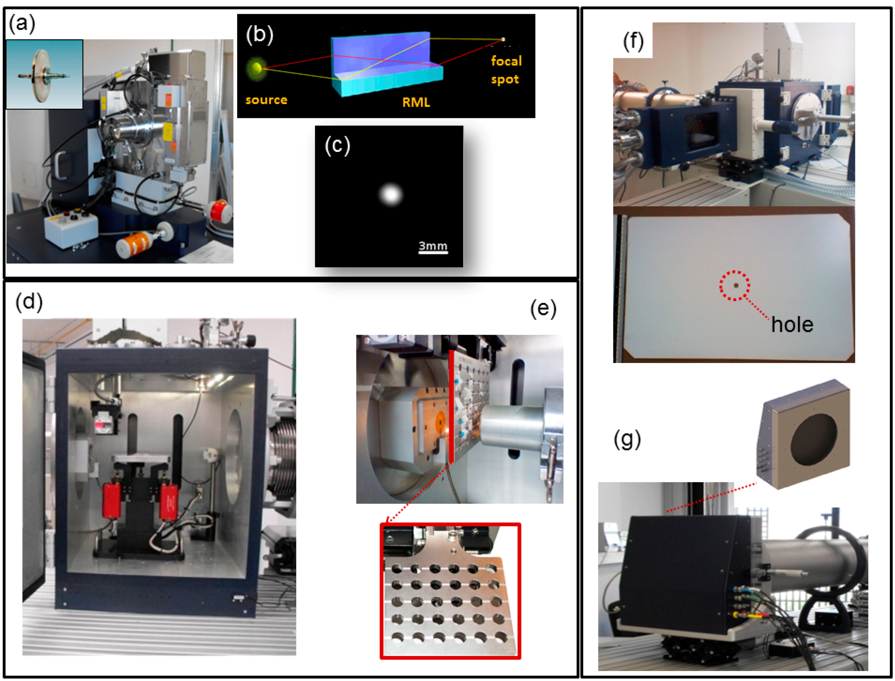
5. A Laboratory Set Up: The XMI-L@b for SAXS/WAXS or GISAXS/GIWAXS Data Collection

Figure 4a shows the rotating anode micro-source installed at the XMI-L@b [37,38,42,43]. The copper target is displayed in the inset of the figure. This laboratory consists of a three-pinhole SAXS/WAXS camera, working in vacuum, with the table-top rotating anode micro-source coupled to a RML confocal optics (Figure 4b) to realize a round shaped sub-millimetric focal spot (minimum size is 70 µm). The image of the focal spot, with specific pinholes, projected at about 2.2 m from the sample, is shown in Figure 4c. For reflection mode geometry, a goniometer is used (Figure 4d) to align the sample surface with respect to the X-ray beam and to tune the penetration depth of the X-ray beam below the surface. This is the typical set-up needed for GISAXS and GIWAXS measurements. The sample holder, for transmission geometry, is displayed in Figure 4e. Kapton or ultralene pockets are used for powders or jelly specimens, glass capillaries or cuvettes are used for liquids.
SAXS/WAXS (or GISAXS/GIWAXS) data at the XMI-L@b are often collected from anisotropic nanomaterials. This definitely requires 2D detectors: an image plate (IP) detector, 250 × 160 mm in size, with 50 or 100 µm effective pixel size and an off-line RAXIA reader, for WAXS data (Figure 4f), as well as a multi wire gas-filled detector with a 1024 × 1024 array, 195 µm pixel size for SAXS data (Figure 4g) are available. The hole in the center of the IP detector (marked with the red circle in Figure 4f) was made on purpose to collect simultaneously, if necessary, WAXS and SAXS data. The concurrence of WAXS and SAXS data collection is sometimes required, for example to keep radiation damage under control by reducing the collection times or to simultaneously collect SAXS/WAXS data on the same sample area.
Several other technical choices are available to set-up a SAXS/WAXS/GISAXS/GIWAXS laboratory. For example, liquid-metal-jet anode electron-impact X-ray micro-sources [44] are today available as valid high brilliance alternatives to rotating anodes; scatterless hybrid metal-single-crystal slits have been proposed with success for small-angle X-ray scattering and high-resolution X-ray diffraction [45]; direct-detection photon counting detector systems such as the PIxeL apparATUs (PILATUS) series of detectors [46], the EIGER detector [47] or the Medipix and PIXcel detectors [48] are definitively a better choice in terms of dynamic range or pixel size.

6. Applications

In the forthcoming paragraphs we describe some practical cases where hard X-rays proved to be an efficient probe to morphologically or structurally characterize inorganic nanomaterials.
-
Combined SAXS and WAXS analysis (Figure 5) allowed us to determine independently particle size/shape and crystalline domain size of silver nanoparticles, dispersed in water. Indeed, nanoparticles can be amorphous, single or multiple crystalline domains. Measuring only SAXS data cannot discriminate between these possibilities. Only the combination of these two techniques can provide a complete answer.
-
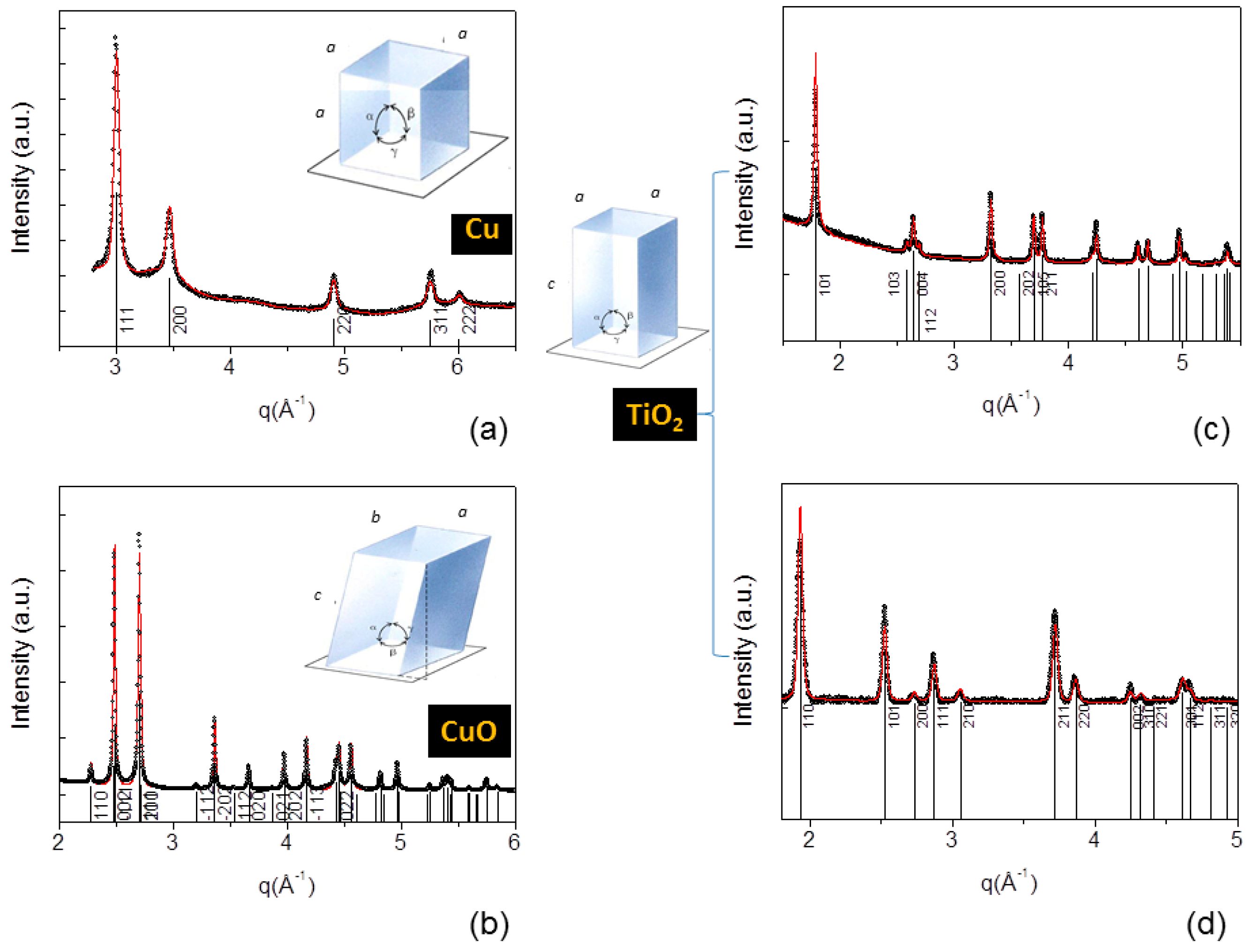
X-ray diffraction (Figure 6) from nanocrystalline powders allowed us to attribute the proper crystal lattice, to refine the lattice unit cell size, to evaluate the crystalline lattice coherence (crystal habit).
-
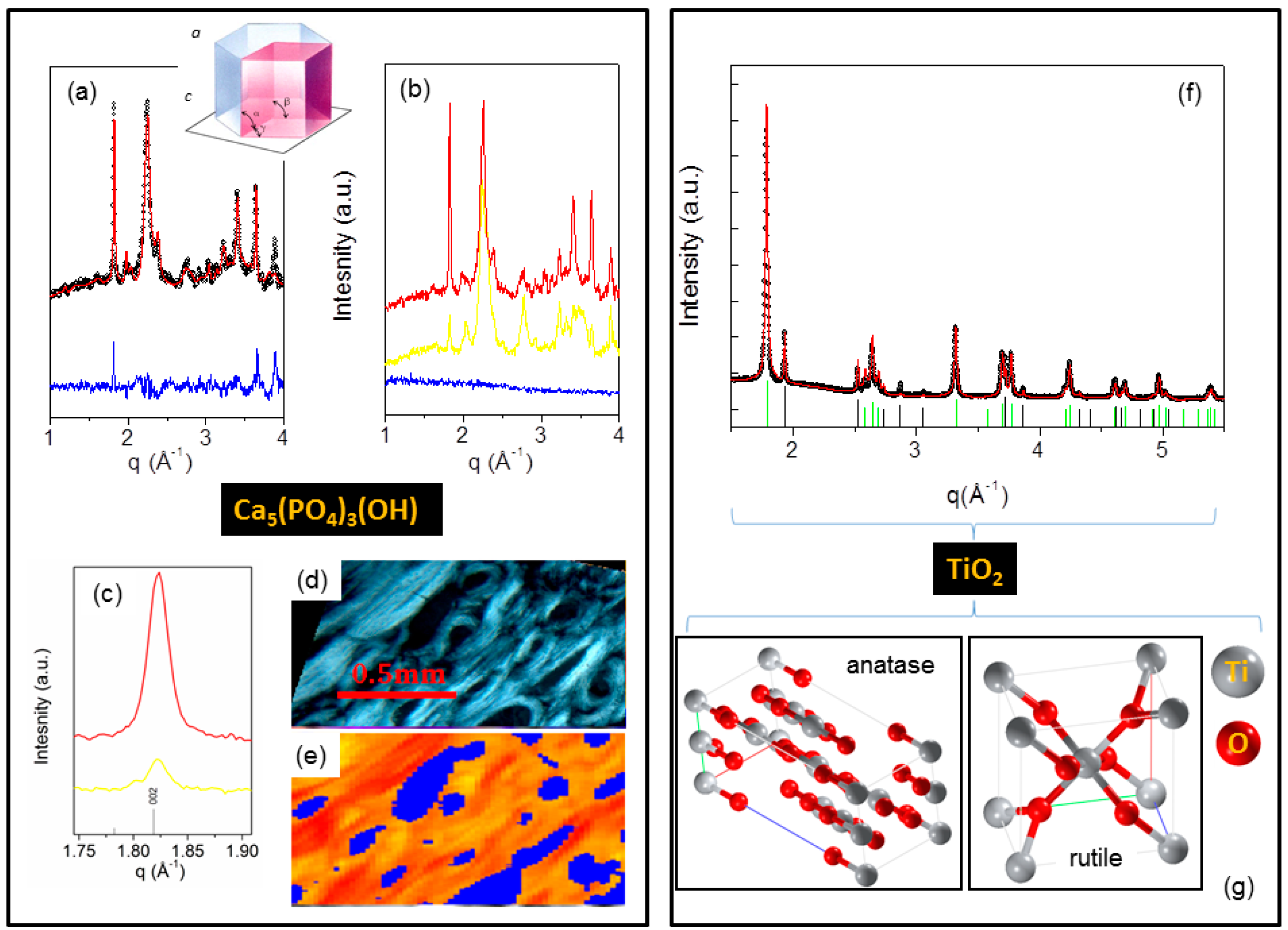
X-ray microdiffraction from bone tissues (Figure 7a–e) was used to identify the hydroxyapatite (HA) crystal structure and to map the orientation of the HA nanocrystals with respect to the collagen fibers.
-
X-ray diffraction (Figure 7f,g) was a means to select and quantify the polymorphs composing a nanocrystalline TiO2 powder.
-
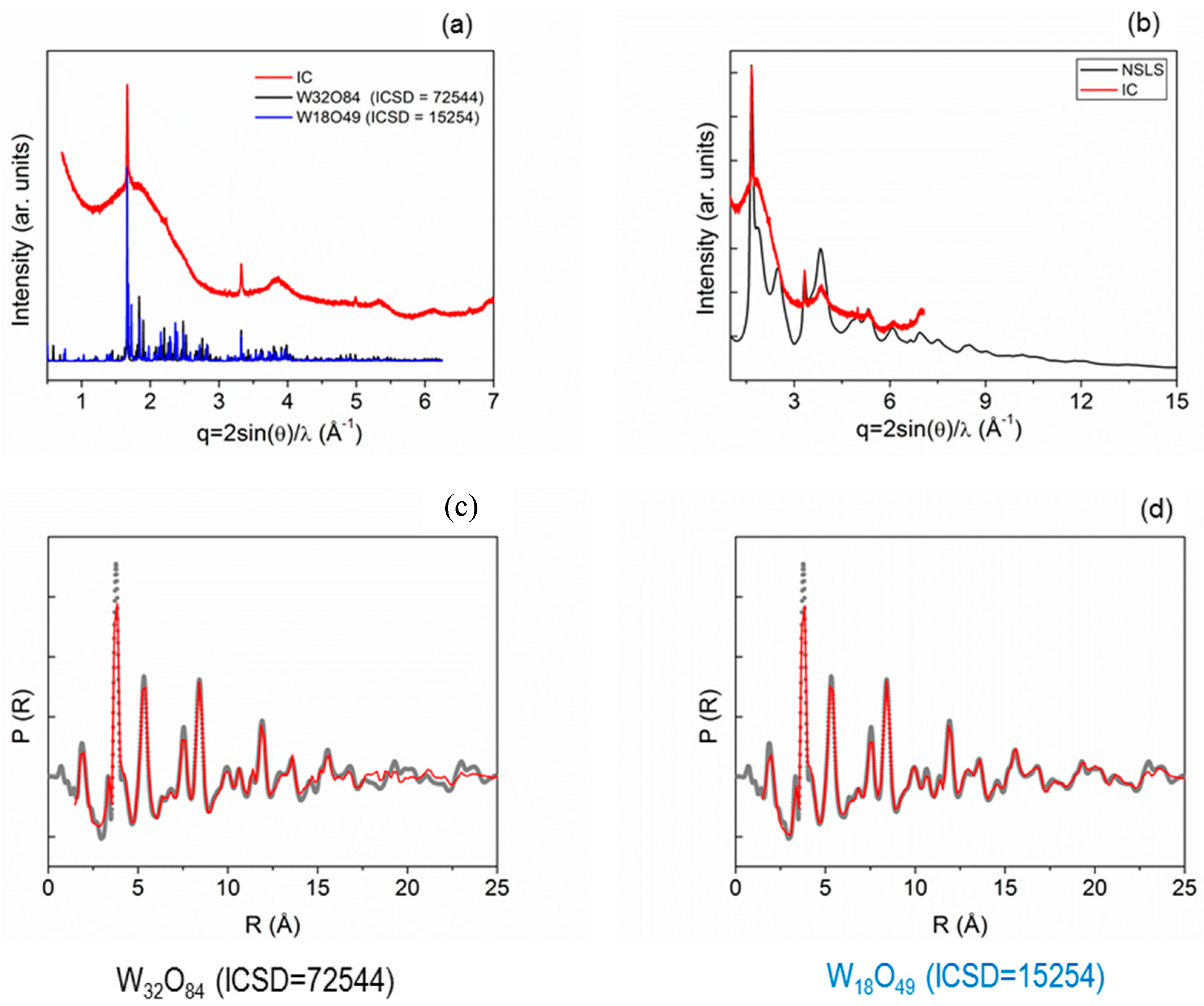
WAXS/atomic PDF analysis (Figure 8) of a tungsten oxide nanomaterial was performed to identify the actual crystalline structure among competitive Magnéli phases.
-
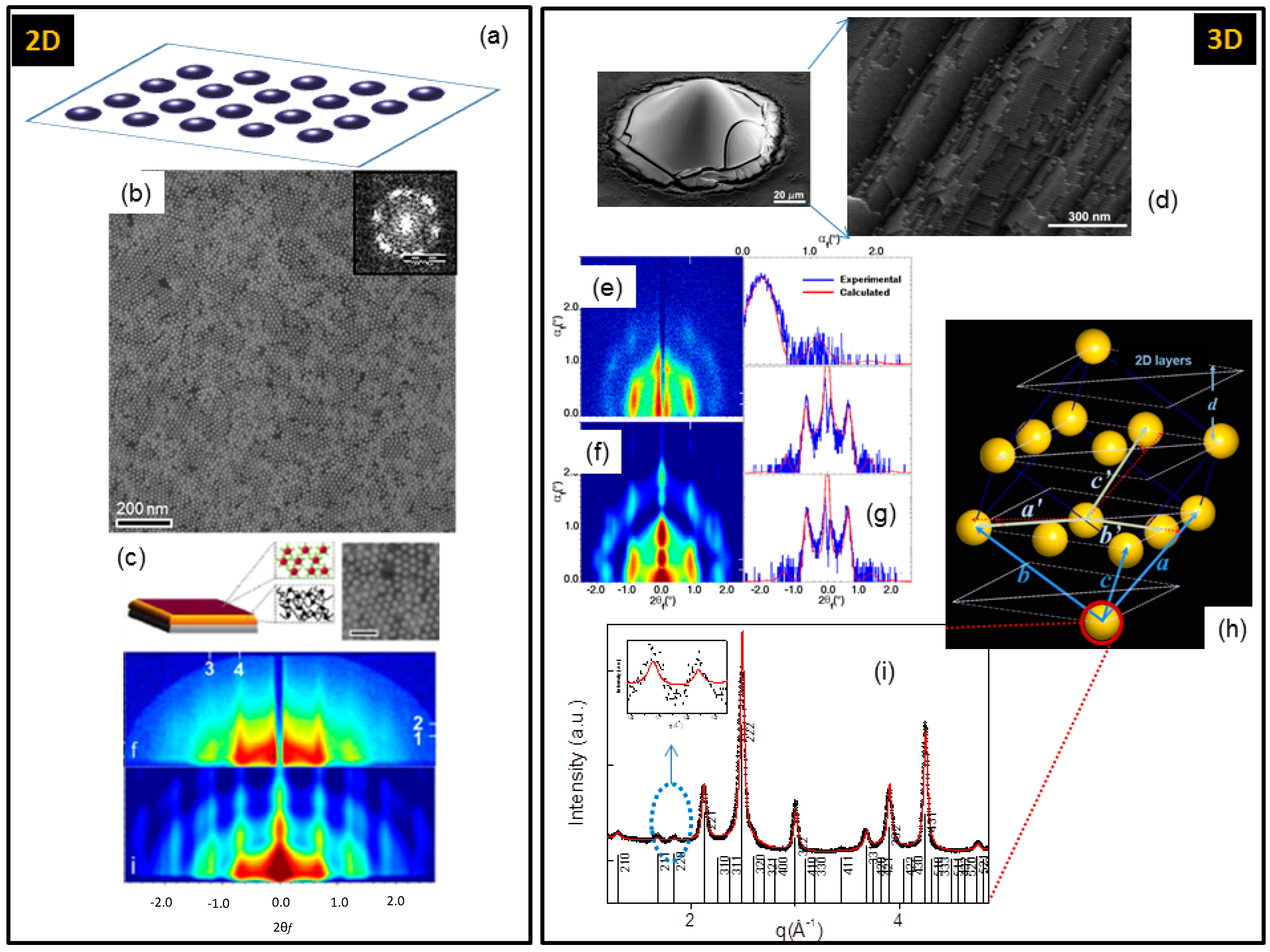
GISAXS and GIWAXS techniques (Figure 9) were chosen to inspect the nanoscale and atomic order of self-assembled 2D or 3D nanocrystal superlattices, respectively.
-
Polystyrene (PS) free standing films containing CdSe/CdS nanocrystals were studied with ptychography, a coherent scanning SAXS technique (Figure 10 and Figure 11), with the aim to map the actual relative position of the nanocrystals embedded, without any periodicity, in 25 µm thick polymers.

7. Nanoparticles in Water

SAXS data of silver nanoparticles are displayed in Figure 5a (dotted pattern) along with the calculated profile (full line). The profile, fitted by means of the GNOM program [49], corresponds to a gyration radius Rg = 8.6 nm and to a distribution of interatomic distances, known as pair distribution function (PDF [50,51,52]), reported in the inset, of nanoparticles with spherical shape. Indeed, the PDF changes with the shape of the scattering objects, as described by the simulations in Figure 5b [53]. The mean size of the nanoparticles, derived from Rg, is D = 2 × √5/3 × Rg ~ 22 ± 1 nm. This value is in close agreement with the Transmission Electron Microscopy (TEM) of the same sample, reported in Figure 5c, showing nanoparticles of spherical shape and mean size (estimated with ImageJ [54]) of 20 ± 2 nm. WAXS data, collected on the same nanoparticles, are displayed as dotted curve in Figure 5d, along with the fitted profile calculated with whole-profile Rietveld-based program FULLPROF [55], as follows: the instrumental resolution function (IRF) was evaluated by fitting the diffraction pattern of a LaB6 NIST standard, recorded under the same experimental conditions as those used for measuring the silver nanoparticles. The IRF data file was provided separately to the program in order to allow subsequent refinement of the diffraction pattern of the sample.
The crystalline phase composition of the sample, namely the ICSD code # 181730, which is a face centered cubic lattice (space group F m − 3 m) with a cubic cell of a = 4.086 Å, was previously determined, provided to the program and refined. The inhomogeneous peak broadening of the diffraction peaks was described by a phenomenological model based on a modified Scherrer formula:
β h , k , l = λ D h , k , l cos θ = λ cos θ i m p a i m p y i m p ( θ h , Φ h )
where β h , k , l is the size contribution to the integral width of the (h,k,l) reflection and y i m p are real spherical harmonics. After refinement of the a i m p coefficients, the program calculated the apparent size of the crystal domains along each reciprocal lattice vector (h,k,l) direction, i.e., D h , k , l . Other refinable parameters were the unit cell parameters. The quality of the obtained fits was checked by means of a goodness-of-fit. The analysis of the WAXS diffraction profile allowed us to determine a crystalline domain elongated along the [111] crystallographic direction, and precisely a domain size of 11.3/6.3 nm along the [111]/[200] directions, respectively. This crystalline domain is reported in scale with respect to the whole nanoparticle spherical size (Figure 5e), as the red colored volume. The spherical shape of the whole nanoparticle (grey region) was ab-initio determined by means of the DUMMIF program [56] from the SAXS data. The comparison in Figure 5e is provided to show that the crystalline domain size is definitively just a portion of the entire particle shape. However, high resolution structural details on crystal facets and rugosity do not correspond to real structural features of the sample, but rather to calculations limits.

8. Nanocrystalline Powders

Often nanocrystals need to be characterized as dried powders. Typical questions concerning the materials are:
-
crystalline structure
-
crystalline domain size
-
multiple crystalline phases
-
possible preferred orientations
Several X-ray powder diffraction profiles, measured from nanocrystals with different lattice symmetries, are here provided: cubic copper [57] (Figure 6a), monoclinic tenorite [58] (Figure 6b), tetragonal anatase [59] (Figure 6c) and rutile [60] (Figure 6d), hexagonal hydroxyapatite [61] (Figure 7a). Table 1 summarizes the data derived from the analysis of the profiles: cell dimensions, domain size along two orthogonal directions. The indexing and fitting of the data was performed with the whole-profile Rietveld-based program FULLPROF [55], following the same procedure explained in Section 6. When a size anisotropy is present the nanocrystal has a non-isotropic domain size, such as for elongated rod-like or flat disk shapes.
Figure 7b shows three different patterns measured from human bone sections: the blue line refers to a background profile, as it does not contain any diffraction peak, while the red and yellow ones correspond to the same hydroxyapatite (HA) crystal structure reported in Figure 7a. The main difference between the red and yellow patterns concerns the 002 reflection, as can be appreciated by Figure 7c. The sharper and more intense peak of the red profile is due to a preferred orientation of the HA nanocrystals, uniaxially oriented along the [002] direction, namely the c-axis, with respect to the yellow profile where the same reflection shows a lower intensity (no preferred orientation). The preferred orientation was monitored across a millimetric sample area either by light microscopy (Figure 7d) or by scanning WAXS microscopy (Figure 7e). The WAXS microscopy shows which of the three WAXS patterns in Figure 7c dominates (blue, red or yellow) in each pixel, or alternatively maps the preferred orientation in the analyzed area. This example concerns experiments performed on healthy and pathologic human bone sections. Here, HA nanocrystals are embedded in collagen fibers within the osteons, forming the bone tissue. The orientation of the HA nanocrystals and of the collagen fibers was investigated by WAXS scanning microscopy and circularly polarized light microscopy (CPL), respectively. Since the red colored regions of the scanning WAXS microscopy correspond to the white areas of the CPL microscopy, we could conclude that the preferred orientation of the HA nanocrystals is coherent with the orientation of the collagen fibers [62].
Figure 7f shows the diffraction pattern of a powder made of TiO2 nanocrystals. TiO2 is known to crystallize in several polymorphs, following a size-dependent thermodynamic stability sequence: rutile → brookite → anatase → TiO2 (B) → two-dimensional lepidocrocite [63]. This study was aimed at determining which crystal structures describe the diffraction pattern and the relative weight fractions. After fitting the experimental data, we drew the conclusion that the investigated sample is a mixture of anatase (green markers) and rutile (black markers) crystal structures (displayed in Figure 7g) in the following percentages: anatase (89%) and rutile (19%). The analysis also provided the cell size and crystalline habit for each crystal structure (not reported). It is not always straightforward to determine the crystalline phase composition of a sample.
The next example describes the case of a tungsten oxide nanomaterial [64] where wide angle X-ray diffraction analysis was realized to identify the exact crystalline structure among possible Magnéli phases [65]. The diffraction pattern in Figure 8a was qualitatively indexed with the orthorhombic W32O84 [66] and the monoclinic W18O49 [67]. Indeed, because of the severe overlapping of the diffraction peaks and because of the extremely anisotropic shape of the nanocrystals (very long rod), the diffraction pattern in Figure 8a contains only three sharp reflections distinguishable from other extremely broad and undefined peaks. In order to disentangle this problem, PDF analysis was performed by collecting diffraction data at the X17A beamline of the National Synchrotron Light Source (NSLS; NSLS-XPD) at Brookhaven National Laboratory. Figure 8b shows the laboratory data (red line) superimposed to the synchrotron data (black line), which were collected at a very short wavelength (λ = 0.18597 Å) to have a good data resolution (as explained in Section 2). The experimental PDF, derived from the NSLS diffraction profile with the PDFgetX3 program [68], is displayed in Figure 8c,d (dotted grey curve) along with the theoretical PDF (red lines) computed with the PDFGui program [69] from the two competitive structures. The best fit in Figure 8d allows the monoclinic W18O49 to be identified as the structure which describes the sample. Here, it is worth clarifying that the atomic pair distribution function, which describes the interatomic distances in the crystals, is extracted from the WAXS data in Figure 8a. Differently, the PDF analysis in the inset of Figure 5a, derived from SAXS data (Figure 5a), has nanoscale resolution and is rather sensitive to the distances between interface points on the object envelope (nanoscale morphological information).

9. Nano-Structured Surfaces

Self-assembly, an essential part of nanotechnology, is a practical strategy for making novel hierarchical complex materials. Hereafter we list some mechanisms and conditions which can drive the self-assembly process [21]:
  • Forces of chemical bonding (covalent, ionic, van der Waals, hydrogen)
  • Physical forces (magnetic, electrostatic, fluidic, ...)
  • Polar/Nonpolar (hydrophobicity)
  • Shape (configurational)
  • Templates (guided self-assembly)
A self-assembly process can result in linear chains of nanostructures (as expanded in Section 9), 2D layers (Figure 9a–c) or 3D ensembles (Figure 9d–g). Figure 9a is a cartoon of a 2D assembly onto a surface. Here, Au nanoparticles (NPs), drop casted onto a suitably functionalized silicon substrate, were found to form a 2D superlattice, extending over micrometers squared areas (Figure 9b), as probed by Scanning Electron Microscopy (SEM). The experimental (upper panel of Figure 9c) GISAXS data were collected at the XMI-L@b to study the nanoscale order of the 2D assembly. The experimental data clearly show the diffraction intensity localized in vertical bars, fingerprint of a two-dimensional organization of the assembled NPs. The fits (lower panel of Figure 9c) allow the inference that the NPs are spherical in shape with a 12 ± 1 nm diameter, in agreement with TEM observations. Moreover, the GISAXS calculated pattern is compatible with a hexagonal symmetry with a = 15.0 ± 0.5 and b = 14.5 ± 0.5 nm in-plane unit cell size [70]. The top inset of Figure 9c describes the teflon layer covering the silicon substrate and a detail of the Au NPs, as observed by TEM. Remarkably, both substrate surface chemistry and size monodispersity of the nanostructures were revealed to be decisive in controlling the extent of the superlattice.
Figure 9d shows a cone-shaped island made of iron oxide nanocrystals self-assembled by a magnetic field onto a silicon substrate [71]. A section of the island, imaged by SEM, revealed a three-dimensional (3D) ordered superlattice, whose lattice symmetry cannot be retrieved from the SEM data in Figure 9d. GISAXS data were collected at the XMI-L@b (Figure 9e) to inspect the packing and symmetry of the nanostructure array. Fitting the experimental data, shown in Figure 9f,g, allowed us to conclude that the iron oxide nanocrystals form a 3D face centered cubic superlattice (Figure 9h), with (111) planes parallel to the substrate. Simulations also revealed that the iron oxide nanocrystals have spherical shape and mean diameter of 9.0 nm, in excellent agreement with results from X-ray diffraction (Figure 9i) and TEM/SEM analyses. Wide angle X-ray diffraction data in Figure 9i could be indexed as maghemite (Fe2O3, space group P 43 3 2) and magnetite (Fe3O4, space group F d−3 m), two crystal structures with the same lattice parameter a = 8.3425 Å. The fit reported in Figure 9i (red line) explained the data as the diffraction from maghemite only. Indeed, the presence of the (211) and (220) peaks with comparable intensities (in the blue circle of Figure 9i and in the inset) is characteristic of maghemite only, so that this phase is certainly present in the sample. However, the presence of magnetite cannot be ruled out, as most of the relevant reflections are overimposed to the maghemite ones (the markers of the magnetite crystal structure are not shown for simplicity).

10. Nanomaterials in Polymers

While in the self-assembled 2D or 3D nanocrystals, described in the previous paragraph, nanocrystals and nanoparticles sit in precise and regular positions, according to the symmetry rules of crystallography, there is another kind of possible self-assembly with a more local order: the so-called end-to-end assembly; here the nanocrystals attach each other to form irregular chains of nanostructures, with very limited and localized periodicity. These materials require the use of coherent X-rays available at dedicated synchrotron radiation beamlines or Free Electron Lasers [72]. In Figure 10 a schematic description of a SAXS experiment with a coherent X-ray beam is provided, to introduce the concept of speckled SAXS pattern. A non-periodic array of nano-objects, described in Figure 10a with the random spheres in the L1 × L2 area, is a gas-like system already discussed in Section 4. The nanometer size of the objects requires investigation by the SAXS technique, although the lack of order (gas-like) gives the typical pattern in Figure 10b, in case of incoherent X-rays. The 2D SAXS pattern, azimuthally integrated, is folded into the 1D SAXS profile (blue line in Figure 10b). From this profile it is possible to determine the mean size and shape of the objects in the L1 × L2 area, but not their relative positions. On the contrary, if the same area is illuminated with coherent X-rays, the corresponding SAXS pattern will be speckled. The speckles in the 2D SAXS patterns, which are the sharp peaks of the corresponding 1D SAXS profile (black line in Figure 10c), are due to the mutual interference of the wavefronts scattered by the random objects in Figure 10a. The speckled pattern contains the same morphological information as with the incoherent X-rays, size and shape of the objects, but additionally encodes also the mutual positions of the nano-objects in space. An analysis of the speckled SAXS profiles, by Fourier transform of the diffraction pattern, allows discrimination among different possibilities, such as those depicted in Figure 10a,d,e. To make an analogy, the coherence of the crystal lattice is substituted by the coherence of the incident wavefront and the Bragg peaks by the speckles. Coherent X-rays are therefore the only solution in the case of an assembly of random nanoscale objects.
A practical application of coherent X-rays is described in Figure 11. Here, polystyrene (PS) free standing films containing CdSe/CdS nanocrystals were studied with coherent X-rays at the cSAXS beamline of the Swiss Light Source (SLS, Villigen, Switzerland) [73].
Figure 11a shows the TEM image of a single octapod standing on a carbon-coated Cu grid with four pods. The cartoon highlights its orientation. A 45°-tilt-SEM image in Figure 11b was collected on a thin nanocomposite film (PS + nanocrystals) deposited onto a SiO2 substrate, after the removal of the PS polymer by oxygen plasma, showing the pod-to-pod attachment of the nanocrystals in short chains. The free standing films were fabricated by mold casting, as sketched in Figure 11c: the injection of the nanocomposite solution into Al molds produces the free-standing thick films, ~25 μm being the average thickness. In order to image the exact packing of the octapods in the free-standing thick films, a reliable non-destructive high resolution imaging technique able to penetrate μm-thick samples and with nanometer resolution is needed. This stringent requirement rules out any electron-based microscopic techniques, as they are not suited for imaging μm-thick films. Hard X-rays on the other hand ensure full penetration in thick polymer foils (even when they are several tens of μm thick), but the non-periodic organization of the NCs in polymers requires a coherent X-ray beam, if a diffractive imaging approach is to be used. Therefore, a technique called ptychography [74,75,76] was adopted to investigate the nanoscale structure of the thick films in transmission mode and with coherent X-rays. Ptychography is a scanning microscopy where the sample is laterally translated across a coherent (here also focused) X-ray beam. Specific overlapping conditions between adjacent scanning positions have to be fulfilled (redundancy). A scattering pattern is recorded at each scanning position (Figure 11d) and it is then used to reconstruct, with nanometric resolution, the object transmission function by means of phase retrieval algorithms [77,78]. Figure 11e shows the object transmission function of a PS film, with 190 Kg/mol molecular weight and 24 ± 4 µm thickness. The reconstructed area is 2.5 × 2.5 µm2 large. A smaller area (870 × 870 nm2) is displayed in Figure 11f. This X-ray-based microscopy technique allowed imaging, with a resolution of 26 nm, of the aggregation of the octapods in interconnected architectures. No other imaging technique can achieve such a resolution on several tens of μm thick films. It should be noted that ptychography is also a label free bio-imaging method, extremely interesting to export to other research fields, for example for cancer studies. Indeed, recently, much interest has been focused on understanding internalization of inorganic nanoparticles in cells as a function of the size and surface chemistry of the nanoparticles as well as of the cell type [79]. One of the most widely used methods to localize the nanoparticles in cells, and distinguish from those internalized from externally adhered particles, is Confocal Laser Scanning Microscopy (CLSM). CLSM allows visualization of nanoparticles in cells at 200 nm resolution, provided that the nanoparticles are marked with a fluorescent molecule, such as rhodamine. Ptychography is expected to map the spatial distribution of any type of “naked” inorganic nanoparticles (quantum dots, magnetic nanoparticles etc.), administered to cells without adding any fluorescent molecules. It is a versatile label free imaging tool, suitable, at least in principle, to study the same model system of nanoparticles internalized in different cell lines.

11. Conclusions and Perspectives

In this article, we discussed X-ray scattering/diffraction techniques to analyze inorganic nanomaterials under different conditions: dispersed in solutions, dried in powders, embedded in matrix, deposited onto surfaces or underneath them. Table-top micro-sources have reduced the gap between laboratory and synchrotron radiation sources, at least concerning ex-situ experiments. Still, most of the research which needs in-situ or in-operando experiments, or multi-techniques, or coherence properties of the X-ray beam, or nano beams, remains in the domain of synchrotron sub-microfocus/nanofocus beamlines. Nanomaterials are today combined with biomaterials, proteins, and polymers to create multi-function hierarchically ordered complex systems. Therefore, X-ray scattering based techniques are showing, more and more, their great potential and effectiveness for the multiple-length-scale structural analysis of nanomaterials.

Acknowledgments

This work was partially financed by EU FP7 project NANoREG, grant 310584, and by the bilateral project CNR/CONICET “TiO2—case in polymeric composite films for food preservation”. Mike Degen, Andrea Fields and Paul Ulrich Pennartz (Rigaku-RIT) are acknowledged for providing pictures of the instrumentation. Stefania Sabella (IIT-Genova), Ing. Francesco Micali (T.C.T. srl—Brindisi), Roberto J. Candal (CONICET—Buenos Aires), Antonio Ancona (CNR-IFN—Bari) are acknowledged for providing samples for SAXS and XRD/WAXS tests. Rocco Lassandro, Brunella Aresta, Lucrezia Cassano, Caterina Chiarella and Giovanni Filograsso are acknowledged for technical and administrative support to the XMI-L@b.

Author Contributions

Cinzia Giannini, Davide Altamura and Teresa Sibillano conceived, designed and performed the experiments; Massimo Ladisa, Dritan Siliqi and Liberato De Caro realized original algorithms to analyze the data; Cinzia Giannini wrote the paper in close collaboration with all the authors.

Conflicts of Interest

The authors declare no conflict of interest.

References

  1. Attwood, D. Soft X-rays and Extreme Ultraviolet Radiation; Cambridge University Press: Cambridge, UK, 1999. [Google Scholar]
  2. Als-Nielsen, J.; McMorrow, D. Elements of Mondern. X-ray Optics; John Wiley & Sons, Ltd.: Chichester, UK, 2000. [Google Scholar]
  3. Arfelli, F.; Bonvicini, V.; Bravin, A.; Cantatore, G.; Castelli, E.; Palma, L.D.; Michiel, M.D.; Fabrizioli, M.; Longo, R.; Menk, R.H.; et al. Mammography with synchrotron radiation: Phase-detection techniques. Radiology 2000, 215, 286–293. [Google Scholar] [CrossRef] [PubMed]
  4. Ambrose, J. Computerized transverse axial scanning (tomography): Part 2. Clinical application. Br. J. Radiol. 1973, 46, 1023–1047. [Google Scholar] [CrossRef] [PubMed]
  5. Peterson, V.K.; Papadakis, C.M. Functional materials analysis using in situ and in operando X-ray and neutron scattering. IUCr J. 2015, 2, 292–304. [Google Scholar] [CrossRef] [PubMed]
  6. Lamberti, C.; Bordiga, S.; Bonino, F.; Prestipino, C.; Berlier, G.; Capello, L.; D’Acapito, F.; Llabre´s Xamena, F.X.; Zecchina, A. Determination of the oxidation and coordination state of copper on different Cu-based catalysts by XANES spectroscopy in situ or in operando conditions. Phys. Chem. Chem. Phys. 2003, 5, 4502–4509. [Google Scholar] [CrossRef]
  7. Metzger, T.; Favre-Nicolin, V.; Renaud, G.; Renevier, H.; Schülli, T. Nanostructures in the Light of Synchrotron Radiation: Surface-Sensitive X-ray Techniques and Anomalous Scattering. In Characterization of Semiconductor Heterostructures and Nanostructures; Elsevier: Oxford, UK, 2008. [Google Scholar]
  8. Zanchet, D.; Hall, B.D.; Ugarte, D. X-ray Characterization of Nanoparticles. In Characterization of Nanophase Materials; Wiley: Atlanta, GA, USA, 2001. [Google Scholar]
  9. Altamura, D.; Sibillano, T.; Siliqi, D.; De Caro, L.; Giannini, C. Grazing Incidence X-ray Studies of Assembled Nanostructured Architectures. Nanomater. Nanotechnol. 2012, 2, Art.16:2012. [Google Scholar]
  10. Miao, J.; Ishikawa, T.; Shen, Q.; Earnest, T. Extending X-ray Crystallography to Allow the Imaging of Noncrystalline Materials, Cells, and Single Protein Complexes. Annu. Rev. Phys. Chem. 2008, 59, 387–410. [Google Scholar] [CrossRef] [PubMed]
  11. Robinson, I.; Harder, R. Coherent X-ray diffraction imaging of strain at the nanoscale. Nat. Mater. 2009, 8, 291–298. [Google Scholar] [CrossRef] [PubMed]
  12. Thibault, P.; Elser, V. X-ray Diffraction Microscopy. Annu. Rev. Condens. Matter Phys. 2010, 1, 237–255. [Google Scholar] [CrossRef]
  13. Holt, M.; Harder, R.; Winarski, R.; Rose, V. Nanoscale Hard X-ray Microscopy Methods for Materials Studies. Annu. Rev. Mater. Res. 2013, 43, 183–211. [Google Scholar] [CrossRef]
  14. Rao, C.N.R.; Biswas, K. Characterization of Nanomaterials by Physical Methods. Annu. Rev. Anal. Chem. 2009, 2, 435–462. [Google Scholar] [CrossRef] [PubMed]
  15. Dorfs, D.; Krahne, R.; Giannini, C.; Falqui, A.; Zanchet, D.; Manna, L. Quantum Dots: Synthesis and Characterization. In Comprehensive Nanoscience and Technology; Elsevier: London, UK, 2011. [Google Scholar]
  16. Garti, N.; Somasundaran, P.; Mezzenga, R. Self-Assembled Supramolecular Architectures: Lyotropic. Liquid Crystals; John Wiley & Sons: Hoboken, NJ, USA, 2012. [Google Scholar]
  17. Grünwald, M.; Geissler, P.L. Patterns without Patches: Hierarchical Self-Assembly of Complex Structures from Simple Building Blocks. ACS Nano 2014, 8, 5891–5897. [Google Scholar] [CrossRef] [PubMed]
  18. Liu, Q.; Sun, Z.; Dou, Y.; Kim, J.H.; Dou, S.X. Two-step self-assembly of hierarchically-ordered nanostructures. J. Mater. Chem. A 2015, 3, 11688–11699. [Google Scholar] [CrossRef]
  19. Ozin, G.A.; Hou, K.; Lotsch, B.V.; Cademartiri, L.; Puzzo, D.P.; Scotognella, F.; Ghadimi, A.; Thomson, J. Nanofabrication by Self-assembly. Mater. Today 2009, 12, 12–23. [Google Scholar] [CrossRef]
  20. Keys, A.S.; Iacovella, C.R.; Glotzer, S.C. Characterizing Structure Through Shape Matching and Applications to Self-Assembly. Annu. Rev. Condens. Matter Phys. 2011, 2, 263–285. [Google Scholar] [CrossRef]
  21. Thiruvengadathan, R.; Korampally, V.; Ghosh, A.; Chanda, N.; Gangopadhyay, K.; Gangopadhyay, S. Nanomaterial processing using self-assembly-bottom-up chemical and biological approaches. Rep. Prog. Phys. 2013, 76, 066501. [Google Scholar] [CrossRef] [PubMed]
  22. Murray, C.B.; Kagan, C.R.; Bawendi, M.G. Synthesis and characterization of monodisperse nanocrystals and close-packed nanocrystal assemblies. Annu. Rev. Mater. Sci. 2000, 30, 545–610. [Google Scholar] [CrossRef]
  23. Giacovazzo, C.; Monaco, H.L.; Viterbo, D.; Scordari, F.; Gilli, G.; Zanotti, G.; Catti, M. Fundamentals of Crystallography; Oxford University Press: Oxford, UK, 2002. [Google Scholar]
  24. Landau, L.D.; Lifshitz, L.M. Quantum Mechanics, Non-Relativistic Theory 3; Pergamon Press: Oxford, UK, 1977. [Google Scholar]
  25. Hohenberg, P.; Kohn, W. Inhomogeneous electron gas. Phys. Rev. 1964, 136, B864–B871. [Google Scholar] [CrossRef]
  26. Abrikosov, A.A.; Gor’kov, L.P.; Dzialoskinskii, I.E. Methods of Quantum Field Theory in Statistical Physics; Dover Publications: Dover, NY, USA, 1994. [Google Scholar]
  27. Thomas, L.H.; Umeda, K. Atomic Scattering Factors Calculated from the TFD Atomic Model. J. Chem. Phys. 1957, 26, 293. [Google Scholar] [CrossRef]
  28. Cromer, D.T.; Mann, J.B. X-ray scattering factors computed from numerical Hartree-Fock wave functions. Acta Cryst. 1968, A24, 321–328. [Google Scholar] [CrossRef]
  29. James Holton. Available online: http://bl831.als.lbl.gov/~jamesh/ (accessed on 26 July 2016).
  30. Bilbao Crystallographic Server. Available online: http://www.cryst.ehu.es/ (accessed on 26 July 2016).
  31. Confalonieri, G.; Dapiaggi, M.; Sommariva, M.; Gateshki, M.; Fitch, A.N.; Bernasconi, A. Comparison of total scattering data from various sources: The case of a nanometric spinel. Powder Diffr. 2015, 30, S65–S69. [Google Scholar] [CrossRef]
  32. Dykhne, T.; Taylor, R.; Florence, A.; Billinge, S.J. Data requirements for the reliable use of atomic pair distribution functions in amorphous pharmaceutical fingerprinting. Pharm. Res. 2011, 28, 1041–1048. [Google Scholar] [CrossRef] [PubMed]
  33. Margaritondo, G. Introduction to Synchrotron Radiation; Oxford: New York, NY, USA, 1988. [Google Scholar]
  34. Reiss, C.A.; Kharchenko, A.; Gateshki, M. On the use of laboratory X-ray diffraction equipment for Pair Distribution Function (PDF) studies. Z. Kristallogr. 2012, 227, 257–261. [Google Scholar] [CrossRef]
  35. Craievich, A.F. Small angle X-ray scattering by nanostructured materials. In Handbook of Sol-Gel Science and Technology, 1st ed.; Sakka, A., Almeida, R., Eds.; Kluwer Publishers: Norwell, MA, USA, 2005; pp. 161–189. [Google Scholar]
  36. Renaud, G.; Lazzari, R.; Leroy, F. Probing surface and interface morphology with Grazing Incidence Small Angle X-ray Scattering. Surf. Sci. Rep. 2009, 64, 255–380. [Google Scholar] [CrossRef]
  37. Altamura, D.; Lassandro, R.; De Caro, L.; Siliqi, D.; Ladisa, M.; Giannini, C. X-ray MicroImaging Laboratory (XMI-LAB). J. Appl. Cryst. 2012, 45, 869–873. [Google Scholar] [CrossRef]
  38. Sibillano, T.; De Caro, L.; Altamura, D.; Siliqi, D.; Ramella, M.; Boccafoschi, F.; Ciasca, G.; Campi, G.; Tirinato, L.; Di Fabrizio, E.; et al. An Optimized Table-Top Small-Angle X-ray Scattering Set-up for the Nanoscale Structural Analysis of Soft Matter. Sci. Rep. 2014, 4, 6985. [Google Scholar] [CrossRef] [PubMed]
  39. Zheng, N.; Yi, Z.; Li, Z.; Chen, R.; Lai, Y.; Men, Y. Achieving grazing-incidence ultra-small-angle X-ray scattering in a laboratory setup. J. Appl. Cryst. 2015, 48, 608–612. [Google Scholar] [CrossRef]
  40. Kirkpatrick, P.; Baez, A.V. Formation of optical images by X-rays. J. Opt. Soc. Am. 1948, 38, 766–774. [Google Scholar] [CrossRef] [PubMed]
  41. Mills, D.; Padmore, H. Report of the Basic Energy Sciences Workshop on X-ray Optics for BES Light Source Facilities. Available online: http://science.energy.gov/bes/community-resources/reports/ (accessed on 26 July 2016).
  42. Corricelli, M.; Altamura, D.; Curri, M.L.; Sibilano, T.; Siliqi, D.; Mazzone, A.; Depalo, N.; Fanizza, E.; Zanchet, D.; Giannini, C.; Striccoli, M. GISAXS and GIWAXS study on self-assembling processes of nanoparticle based superlattices. CrystEngComm 2014, 16, 9482–9492. [Google Scholar] [CrossRef]
  43. De Caro, L.; Altamura, D.; Sibillano, T.; Siliqi, D.; Filograsso, G.; Bunk, O.; Giannini, C. Rat-tail tendon fiber SAXS high-order diffraction peaks recovered by a superbright laboratory source and a novel restoration algorithm. J. Appl. Cryst. 2013, 46, 672–678. [Google Scholar] [CrossRef]
  44. Hemberg, O.; Otendal, M.; Hertz, H.M. Liquid-metal-jet anode electron-impact X-ray source. Appl. Phys. Lett. 2003, 83, 1483. [Google Scholar] [CrossRef]
  45. Li, Y.; Beck, R.; Huang, T.; Choi, M.C.; Divinagracia, M. Scatterless hybrid metal-single-crystal slit for small-angle X-ray scattering and high-resolution X-ray diffraction. J. Appl. Cryst. 2008, 41, 1134–1139. [Google Scholar] [CrossRef]
  46. Kraft, P.; Bergamaschi, A.; Broennimann, C.; Dinapoli, R.; Eikenberry, E.F.; Henrich, B.; Johnson, I.; Mozzanica, A.; Schlepütz, C.M.; Willmott, P.R.; et al. Performance of single-photon-counting PILATUS detector modules. J. Synch. Rad. 2009, 16, 368–375. [Google Scholar] [CrossRef] [PubMed]
  47. Johnson, I.; Bergamaschi, A.; Buitenhuis, J.; Dinapoli, R.; Greiffenberg, D.; Henrich, B.; Ikonen, T.; Meier, G.; Menzel, A.; Mozzanica, A.; et al. Capturing dynamics with Eiger, a fast-framing X-ray detector. J. Synch. Rad. 2012, 19, 1001–1005. [Google Scholar] [CrossRef] [PubMed]
  48. Campbell, M. 10 years of the Medipix2 Collaboration. Nucl. Instr. Meth. A 2011, 633, S1–S10. [Google Scholar] [CrossRef]
  49. Svergun, D.I. Determination of the regularization parameter in indirect-transform methods using perceptual criteria. J. Appl. Cryst. 1992, 25, 495–503. [Google Scholar] [CrossRef]
  50. Egami, T.; Billinge, S.J.L. Underneath the Bragg Peaks—Structural Analysis of Complex Materials; Pergamon: London, UK, 2012. [Google Scholar]
  51. Glatter, O. The interpretation of real-space information from small-angle scattering experiments. J. Appl. Cryst. 1979, 12, 166–175. [Google Scholar] [CrossRef]
  52. Glatter, O. Determination of particle-size distribution functions from small-angle scattering data by means of the indirect transformation method. J. Appl. Cryst. 1980, 13, 7–11. [Google Scholar] [CrossRef]
  53. Giannini, C.; Siliqi, D.; Altamura, D. Nanomaterial Characterization By X-Ray Scattering Techniques. In Nanocomposites: In Situ Synthesis of Polymer-Embedded Nanostructures; Wiley: Oboken, NJ, USA, 2013. [Google Scholar]
  54. ImageJ—Image Processing and Analysis in Java. Available online: https://imagej.nih.gov/ij/ (accessed on 26 July 2016).
  55. Rodriguez-Carvajal, J. Recent advances in magnetic structure determination by neutron powder diffraction. Phys. B 1993, 192, 55–69. [Google Scholar] [CrossRef]
  56. Franke, D.; Svergun, D.I. DAMMIF, a program for rapid ab-initio shape determination in small-angle scattering. J. Appl. Cryst. 2009, 42, 342–346. [Google Scholar]
  57. Straumanis, M.E.; Yu, L.S. Lattice parameters, densities, expansion coefficients and perfection of structures of Cu and Cu-In alpha phase. Acta. Cryst. A 1969, 25, 676–682. [Google Scholar] [CrossRef]
  58. Massarotti, V.; Capsoni, D.; Bini, M.; Altomare, A.; Moliterni, A.G.G. X-ray powder diffraction ab initio structure solution of materials from solid state synthesis: The copper oxide case. Z. Kristallogr. 1998, 213, 259–265. [Google Scholar] [CrossRef]
  59. Petronella, F.; Curri, M.L.; Striccoli, M.; Mateo-Mateo, C.; Alvarez-Puebla, R.A.; Sibillano, T.; Giannini, C.; Correa-Duarte, M.A.; Comparelli, R. Direct growth of shape controlled TiO2 nanocrystals onto SWCNTs for highly active photocatalytic materials in the visible. Appl. Cat. B: Environ. J. 2015, 178, 91–99. [Google Scholar] [CrossRef]
  60. Lynch, J.; Giannini, C.; Cooper, J.; Sharp, J.; Buonsanti, R. Substitutional or interstitial site-selective nitrogen doping in TiO2 nanostructures. J. Phys. Chem. C 2015, 119, 7443–7452. [Google Scholar] [CrossRef]
  61. Kay, M.I.; Young, R.A.; Posner, A.S. Crystal structure of hydroxyapatite. Nature 1964, 25, 1050–1052. [Google Scholar] [CrossRef]
  62. Giannini, C.; Siliqi, D.; Bunk, O.; Beraudi, A.; Ladisa, M.; Altamura, D.; Stea, S.; Baruffaldi, F. Correlative light and scanning X-ray Scattering microscopy of healthy and pathologic human bone sections. Sci. Rep. 2012, 2, 435. [Google Scholar] [CrossRef] [PubMed]
  63. Vittadini, A.; Sedona, F.; Agnoli, S.; Artiglia, L.; Casarin, M.; Rizzi, G.A.; Sambi, M.; Granozzi, G. Stability of TiO2 Polymorphs: Exploring the Extreme Frontier of the Nanoscale. Chemphyschem 2010, 11, 1550–1557. [Google Scholar] [CrossRef] [PubMed]
  64. Caliandro, R.; Sibillano, T.; Belviso, B.D.; Scarfiello, R.; Hanson, J.C.; Dooryhee, E.; Manca, M.; Cozzoli, P.D.; Giannini, C. Static and dynamical structural investigations of metal-oxide nanocrystals by powder X-ray diffraction: Colloidal tungsten oxide as a case of study. Chemphyschem 2016, 17, 699–709. [Google Scholar] [CrossRef] [PubMed]
  65. Migas, D.B.; Shaposhnikov, V.L.; Borisenko, V.E. Tungsten oxides. II. The metallic nature of Magnéli phases. J. Appl. Phys. 2010, 108, 093714. [Google Scholar] [CrossRef]
  66. Barabanenkov, Y.A.; Val’kovskii, M.D.; Zakharov, N.D.; Zibrov, I.P.; Popov, A.I.; Filonenko, V.P. Structure of tungsten oxide W O2.625 (W32 O84). Russ. J. Inorg. Chem. 1992, 37, 9–12. [Google Scholar]
  67. Viswanathan, K.; Brandt, K.; Salje, E. Crystal structure and charge carrier concentration of W18 O49. J. Solid State Chem. 1981, 36, 45–51. [Google Scholar] [CrossRef]
  68. Juhas, P.; Davis, T.; Farrow, C.L.; Billinge, S.J.L. PDFgetX3: A rapid and highly automatable program for processing powder diffraction data into total scattering pair distribution functions. J. Appl. Cryst. 2013, 46, 560–566. [Google Scholar] [CrossRef]
  69. Farrow, C.L.; Juhas, P.; Liu, J.W.; Bryndin, D.; Božin, E.S.; Bloch, J.; Proffen, Th.; Billinge, S.J.L. PDFfit2 and PDFgui: Computer programs for studying nanostructure in crystals. J. Phys. Condens. Matter 2007, 19, 335219. [Google Scholar] [CrossRef] [PubMed]
  70. Corricelli, M.; Depalo, N.; Fanizza, E.; Altamura, D.; Giannini, C.; Siliqi, D.; Di Mundo, R.; Palumbo, F.; Agostiano, A.; Striccoli, M.; et al. 2D Plasmonic Superlattice Based on Au Nanoparticles Self-Assembling onto a Functionalized Substrate. J. Phys. Chem. C 2014, 118, 7579–7590. [Google Scholar] [CrossRef]
  71. Altamura, D.; Holy, V.; Siliqi, D.; Lekshimi, I.C.; Nobile, C.; Maruccio, G.; Cozzoli, P.D.; Fan, L.; Gozzo, F.; Giannini, C. Exploiting GISAXS for the study of 3D ordered superlattice of self-assembled colloidal iron oxide nanocrystals. Cryst. Growth Des. 2012, 12, 5505–5512. [Google Scholar] [CrossRef]
  72. Ribic, P.R.; Margaritondo, G. Status and prospects of X-ray free-electron lasers (X-FELs): A simple presentation. J. Phys. D: Appl. Phys. 2012, 45, 213001. [Google Scholar] [CrossRef]
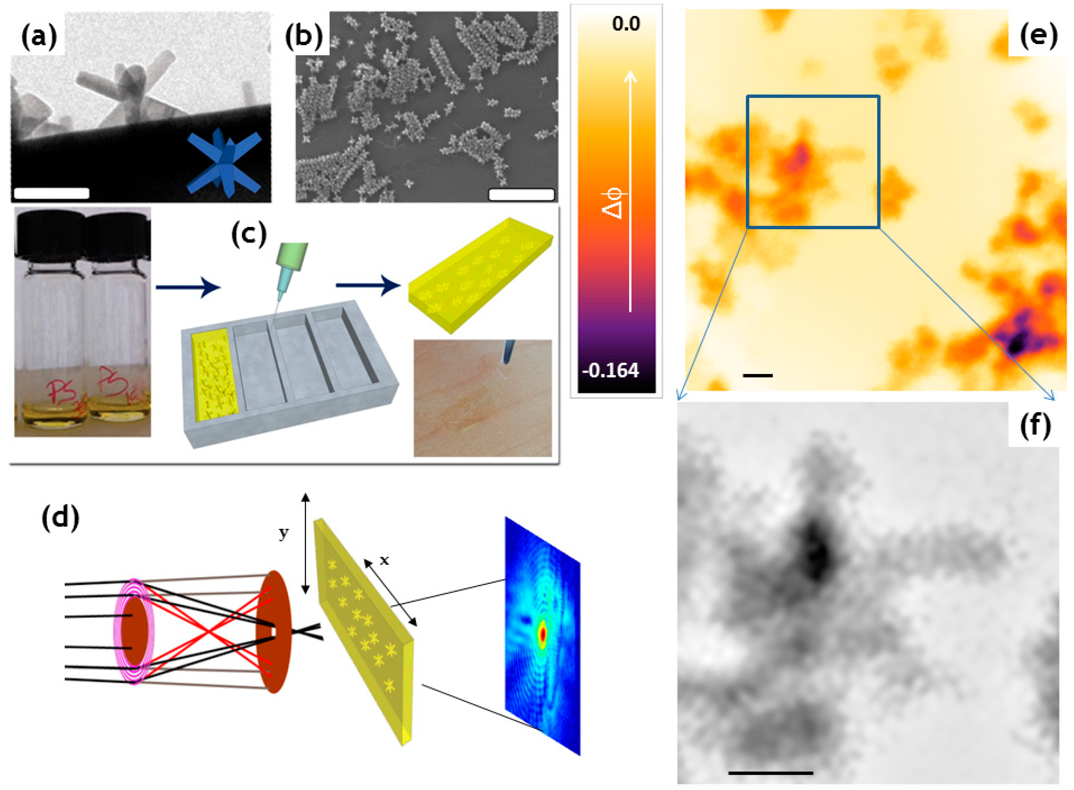
  73. De Caro, L.; Altamura, D.; Arciniegas, M.; Siliqi, D.; Kim, M.R.; Sibillano, T.; Manna, L.; Giannini, C. Ptychographic Imaging of Branched Colloidal Nanocrystals Embedded in Free-Standing Thick Polystyrene Films. Sci. Rep. 2016, 6, 19397. [Google Scholar] [CrossRef] [PubMed]
  74. Rodenburg, J.M.; Hurst, A.C.; Cullis, A.G.; Dobson, B.R.; Pfeiffer, F.; Bunk, O.; David, C.; Jefimovs, K.; Johnson, I. Hard-X-ray Lensless Imaging of Extended Objects. Phys. Rev. Lett. 2007, 98, 034801. [Google Scholar] [CrossRef] [PubMed]
  75. Thibault, P.; Dierolf, M.; Menzel, A.; Bunk, O.; David, C.; Pfeiffer, F. High-Resolution Scanning X-ray Diffraction Microscopy. Science 2008, 321, 379–382. [Google Scholar] [CrossRef] [PubMed]
  76. Dierolf, M.; Menzel, A.; Thibault, P.; Schneider, P.; Kewish, C.M.; Wepf, R.; Bunk, O.; Pfeiffer, F. Ptychographic X-ray computed tomography at the nanoscale. Nature 2010, 467, 436–439. [Google Scholar] [CrossRef] [PubMed]
  77. Fienup, J.R. Phase retrieval algorithms: A comparison. Appl. Opt. 1982, 21, 2758–2769. [Google Scholar] [CrossRef] [PubMed]
  78. Fienup, J.R. Phase retrieval algorithms: A personal tour. Appl. Opt. 2013, 52, 45–56. [Google Scholar] [CrossRef] [PubMed]
  79. Gottstein, C.; Wu, G.; Wong, B.J.; Zasadzinski, J.A. Precise Quantification of Nanoparticle Internalization. ACS Nano 2013, 7, 4933–4945. [Google Scholar] [CrossRef] [PubMed]
Figure 1. (a) On the top is the atomic scattering factor formula, in the center a scattering atom, at the bottom the scattering vector, i.e., the difference between diffracted ( k d ) and incoming ( k i ) wave vectors; (b) atomic scattering factors for oxygen (Z = 8), silicon (Z = 14) and titanium (Z = 22), evaluated for Cu Kα1, i.e., λ = 1.540562 Å (full lines), and for Mo Kα1, i.e., λ = 0.71072 Å (dotted lines).
Crystals 06 00087 g001
Figure 2. (a) Hexagonal ring of carbon atoms; and (b) its molecular form factor (λ = 1.540562 Å, detector pixel size = 100 µm, linear detector size = 20 cm; sample-to-detector distance = 5 cm).
Crystals 06 00087 g002
Figure 3. (a) Body centered cubic nickel lattice (ICSD database code 183264, i.e., a = b = c = 2.81 Å, α = β = γ = 90° and space group = I m − 3 m); (b) face centered cubic nickel lattice (ICSD database code 181716, i.e., a = b = c = 3.227 Å, α = β = γ = 90° and space group = F m − 3 m); (c) simulated diffraction patterns for the ICSD 183264 structure; (d) simulated diffraction patterns for the ICSD 181716 stucture. The simulated profiles are computed for a crystalline box containing 3 × 3 × 3 (black profile), 10 × 10 × 10 (red profile) and 30 × 30 × 30 (green profile) unit cells. Wavelength used for calculation: λ = 1.540562 Å.
Crystals 06 00087 g003
Figure 4. Different images of the XMI-L@b. (a) table-top rotating anode; (b) reflective multilayer (RML) confocal optics; (c) round shaped sub-millimetric focal beam spot; (d) sample chamber and GISAXS/GIWAXS goniometer; (e) sample holder for SAXS/WAXS data; (f) image plate (IP) detector, 250 × 160 mm in size, with 50 or 100 µm effective pixel size and off-line RAXIA reader, for WAXS data; (g) multi wire gas-filled detector with a 1024 × 1024 array, 195 µm pixel size for SAXS data. Partially reprinted with permission of the International Union of Crystallography from reference [37].
Crystals 06 00087 g004
Figure 5. (a) SAXS data of silver nanoparticles dispersed in water, with pair distribution function (PDF) of scattering objects with spherical shape (inset); (b) SAXS (up) and PDF (down) simulated profiles for scattering objects of different shape (grey: full sphere, red: cylinder, green: prism, blue: disk; cyan: hollow sphere; magenta: dumbbell); (c) Transmission electron microscopy (TEM) image of the sample reported in (a); (d) WAXS data (dotted curve) collected on the sample in (a) and the corresponding fitted profile (red line) calculated for the silver crystal structure, ICSD code # 181730, face centered cubic lattice (space group F m−3 m) with a cubic cell of a = 4.086 Å; (e) crystalline domain (red colored volume) extracted from WAXS data analysis, reported in scale with respect to the whole nanoparticle spherical size (grey full sphere) extracted from SAXS data analysis. Partially reprinted with permission from reference [53].
Crystals 06 00087 g005
Figure 6. X-ray powder diffraction profiles measured from cubic copper (a) monoclinic tenorite; (b) tetragonal anatase; (c) and rutile; (d) nanocrystals. The dotted curves represent the experimental data, the red lines the fitted profiles. Experiments were performed by using a Bruker D8-Discover diffractometer, in reflection mode, with Cu Kα1 radiation, i.e., λ = 1.540562 Å.
Crystals 06 00087 g006
Figure 7. (a) X-ray powder diffraction profiles hexagonal hydroxyapatite nanocrystals measured from healthy and pathologic human bone sections. Dotted curves are the experimental data, red lines the fitted profiles. Experiments were performed at the cSAXS beamline of the SLS synchrotron source, in transmission scanning mode with λ = 0.6673 Å; (b) blue line is the background profile, red and yellow ones correspond to the same hydroxyapatite (HA) crystal structure as in (a), with/without (red/yellow) preferred orientation; (c) zoom of the (002) reflection from the whole patterns in (b); (d) Light microscopy of the same sample in (a); (e) scanning WAXS microscopy of the same sample in (a); (f) X-ray powder diffraction profile measured from a powder mixture of anatase and rutile nanocrystals. Dotted curve is the experimental data, red line the fitted profile. Experiments are performed with a Bruker D8-Discover diffractometer, in reflection mode, with Cu Kα1 radiation, i.e., λ = 1.540562 Å. (g) anatase and rutile crystal structures. Partially reprinted with permission from reference [62].
Crystals 06 00087 g007
Figure 8. (a) X-ray diffraction (XRD) pattern of a WOx rod-like material, indexed with two different Magnéli phases: the orthorhombic W32O84 (ICSD #72544) and the monoclinic W18O49 (ICSD #15254); (b) diffraction data collected in transmission scanning mode with λ = 0.18597 Å at the X17A beamline of the National Synchrotron Light Source (NSLS; NSLS-XPD) at Brookhaven National Laboratory (black line) compared to laboratory data (red line) collected with a Bruker D8-Discover diffractometer, in reflection mode, with Cu Kα1 radiation, i.e., λ = 1.540562 Å; (c) experimental PDF (dotted grey curve), derived from the NSLS diffraction profile in (b), and theoretical PDF (red lines) computed from the W32O84 (ICSD #72544); (d) experimental PDF (dotted grey curve) and theoretical PDF (red lines) computed from the W18O49 (ICSD #15254). Partially reprinted with permission from reference [64].
Crystals 06 00087 g008
Figure 9. (a) a cartoon of a 2D assembly onto a surface; (b) Scanning Electron Microscopy (SEM) image of Au nanoparticles (NPs), drop casted onto a teflon functionalized silicon substrate, described by the top inset in (c); (c) experimental/calculated (upper/lower image) GISAXS data, collected at the XMI-L@b, and a detail of the Au NPs, as observed by TEM; (d) cone-shaped island made of iron oxide nanocrystals self-assembled by magnetic field onto a silicon substrate (left) and section of the island, imaged by SEM (right); (eg) experimental and calculated GISAXS data; (h) 3D face centered cubic lattice, with (111) planes parallel to the substrate; (i) X-ray powder diffraction profile measured from the same sample in (a). Dotted curve is the experimental data, red line the fitted profile. The zoom in the inset corresponds to the (211) and (220) peaks with comparable intensities (in the blue circle of Figure 9i) which are characteristic of maghemite structure. Experiments are performed at the MS beamline of the SLS synchrotron source, in reflection mode, with λ = 0.495722 Å. Partially reprinted with permission from reference [70,71].
Crystals 06 00087 g009
Figure 10. (a) non-periodic array of nano-objects, random spheres, in a L1 × L2 area; (b) schematic 2D and 1D (blue line) SAXS pattern, if incoherent X-rays are used to illuminate the sample in (a); (c) schematic 2D and 1D (blue line) SAXS speckled pattern, if coherent X-rays are used to illuminate the sample in (a); (d,e) same nano-objects as in (a), located in different positions.
Crystals 06 00087 g010
Figure 11. (a) TEM image of a single octapod standing on a carbon-coated Cu grid with four pods. The cartoon highlights its orientation; (b) 45°-tilt-SEM of a thin nanocomposite film (PS + nanocrystals) deposited onto a SiO2 substrate, after the removal of the polystyrene (PS) polymer by oxygen plasma; (c) free standing films fabrication by mould casting; (d) diffraction pattern recorded in ptychographic mode; (e) object transmission function of a PS film, with 190 Kg/mol molecular weight and 24 ± 4 µm thickness, as obtained after phase retrieval of the ptychographic data (reconstructed area is 2.5 × 2.5 µm2); (f) smaller area (870 × 870 nm2) of (e). Scale bar is 200 nm. Partially reprinted with permission from reference [73].
Crystals 06 00087 g011
Table 1. Data derived from the analysis of the profiles in Figure 6a–d and in Figure 7a: a, b, c cell edges, domain size along two orthogonal directions. When a size anisotropy is present the nanocrystal has a non-isotropic habit, such as for elongated rod-like or flat disk shapes.
Crystal LatticeMaterialSpace Groupa,b,c [Å]Size [Å]Size [Å]
CubicCu-copperF m−3 ma = b = c = 3.623159 [111]95 [200]
MonoclinicCuO-tenoriteC 2/ca = b = 4.685
c = 5.128
244244
TetragonalTiO2-anataseI 41/a m da = b = 3.784
c = 9.508
162 [200]139 [004]
TetragonalTiO2-rutileP 42/m n ma = b = 4.597
c = 2.958
233233
HexagonalCa5(PO4)3(OH)-hydroxyapatiteP 63/ma = b = 9.465
c = 6.9095
210 [002]25 [110]

