Size and Shape Evolution of GaAsSb-Capped InAs/GaAs Quantum Dots: Dependence on the Sb Content


1
Department of Physics and Astronomy, College of Sciences, King Saud University, Riyadh 11451, Saudi Arabia
2
School of Electrical and Electronic Engineering, The University of Manchester, Sackville Street, Manchester M139PL, UK
3
National Center for Nanotechnology and advanced materials, KACST, Riyadh 11442, Saudi Arabia
*
Author to whom correspondence should be addressed.
Crystals 2019, 9(10), 530; https://0-doi-org.brum.beds.ac.uk/10.3390/cryst9100530
Submission received: 18 September 2019
/
Revised: 8 October 2019
/
Accepted: 12 October 2019
/
Published: 15 October 2019
(This article belongs to the Special Issue Nanowires and Quantum Dots for IoT Applications)
Abstract
:Capping InAs/GaAs quantum dots (QDs) with a thin GaAsSb layer alters the QDs structural properties, leading to considerable changes in their optical properties. The increase of the Sb content induces a redshift of the emission energies, indicating a change in the buried QDs shape and size. The presence of well-defined ground- and excited-state emission bands in all the photoluminescence spectra allow an accurate estimation of the buried QDs size and shape by numerical evaluation and tuning of the theoretical emission energies. For an Sb content below 14%, the QDs are found to have a type I band alignment with a truncated height pyramidal form. However, for higher Sb content (22%), the QDs are present in a full pyramidal shape. The observed behavior is interpreted in terms of increasing prevention of InAs QDs decomposition with increasing the Sb content in the cap layer.
1. Introduction
Self-Assembled InAs QDs have been, to date, a subject of intense research efforts dedicated to exploit their unique properties for diverse innovative applications including, lasers [1], detectors [2] and solar cells [3]. Covering InAs QDs with a GaAsSb capping layer (CL) has in particular been found to be interesting to extend their emission beyond telecom optical wavelength bands [4,5,6]. In addition to the strain reduction around the QDs, conventionally performed by InGaAs alloy [7], GaAsSb CL has been experimentally demonstrated to reduce the decomposition of QDs during the capping process [8]. For Sb contents (XSb) lower than 14%, which allow the GaAsSb-capped InAs QDs to have a type I band alignment, the reduction of both strain and decomposition effects, leads to an increased height, longer emission wavelength, and better luminescence efficiency [9,10]. However, for higher Sb content, a type-II band alignment occurs, giving rise to a longer emission wavelength [10] with most-likely degradation of the capping-layer properties [11]. Thus, capping InAs QD with GaAsSb has numerous advantages, including the increase of the QD size as well as tailoring the band lineup, paving the way to novel applications. Accordingly, an intensive experimental and computational work has been performed to understand and optimize the QD structures.
Most of the available reports, including computational modeling, aim to confirm the cross-over composition, allowing the band alignment to transit from type I to type II [12,13,14], the strain around the QD [15] and the consequent impact on the carriers’ recombination time [16]. However, less attention has been paid to the influence of the Sb content of the GaAsSb CL on the evolution of the QD size and shape [8,10].
In this work, we have combined photoluminescence spectroscopy and numerical modeling to investigate the effect of Sb content variation on the size and shape of GaAsSb-capped InAs QDs. The obtained results confirm the literature-reported structural investigation and show the ability to gain useful information on the buried InAs/GaAsSb dots size and shape in a low-cost and nondestructive way by combining a simple numerical model with photoluminescence measurements.
2. Materials and Methods
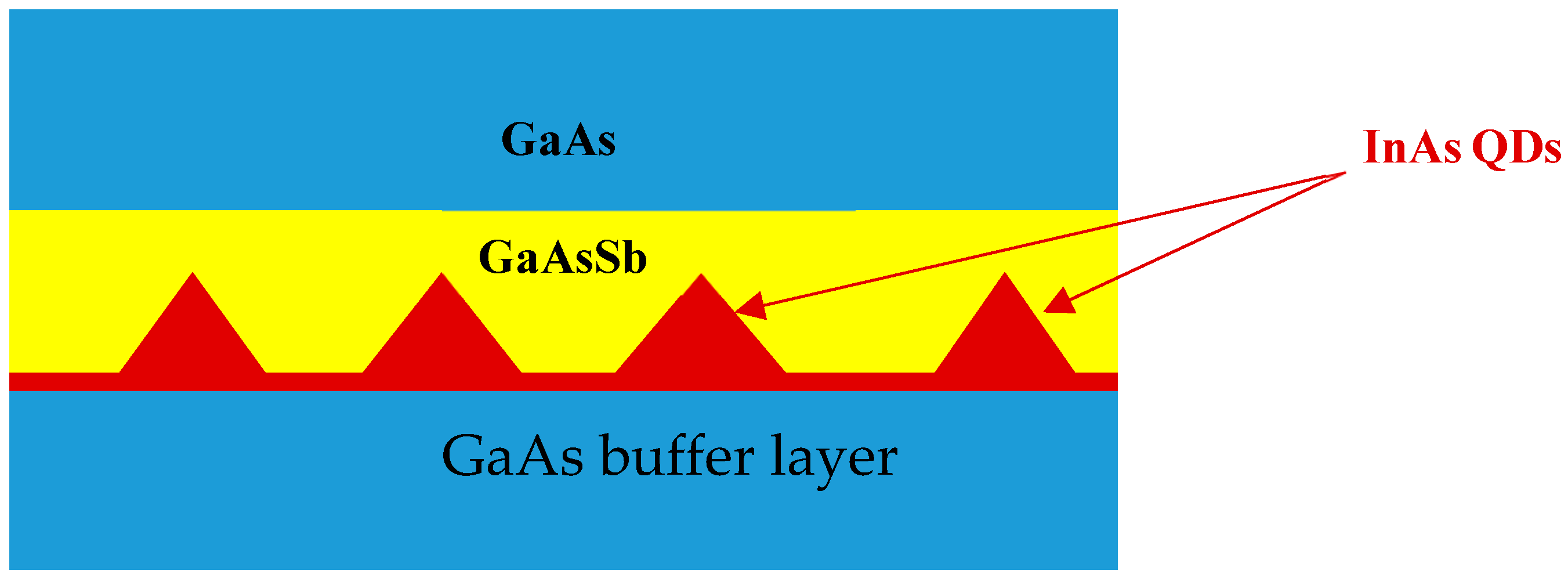
The samples are grown by Molecular Beam Epitaxy on p-type GaAs substrate. They consist of InAs QDs formed upon deposition of 2.5 MLs-thick InAs material on a 200 nm-thick GaAs buffer layer and capped with 6 nm-thick GaAsSb strain-reducing layer, followed by a 44 nm-thick GaAs layer. Four samples are prepared with different Sb contents in the CL. Namely, XSb = 0%, 6%, 12% and 22%. These samples are studied by 77 K continuous-wave PL spectroscopy. More details on the samples growth procedure and characterization can be found in [17]. A schematic of the investigated structure is shown in Figure 1.
For simplicity of the calculation, we adopted the single-band constant potential model where the carriers confined energies are supposed to be dominantly governed by the size quantization effect [18]. Despite the adopted approximations, this model still retains key elements of the essential physics [19], allowing comparable results to more sophisticated models [18,19] and comprehensive interpretation and analysis of experimental data relative to InAs QDs in the GaAs matrix [18]. Therefore, it falls within the goal of this work, intending to gain useful information permitting accurate tracking of the CL Sb content-induced evolution of buried QD size and shape.
In order to extract valuable information on the buried QDs shape and size, the ground and excited states emission energies from the GaAsSb-capped InAs QDs are numerically driven by solving the three-dimensional Schrödinger equation in Cartesian coordinates by a finite elements method in the frame of the single-band effective mass approximation [18,20].
The Schrödinger equation is given by:
m*, and ζ represent the carrier’s effective mass, confined energy levels and wave function, respectively. r and V are the Cartesian coordinates’ vector and the confining potential barrier.
Equation (1) has been solved for the electrons in the conduction band and heavy holes in the valence band considering the lattice-mismatch-induced strain. The material parameters used in this calculation are taken from [21], and those of GaAsSb are driven by linear interpolation from its binary constituent materials. The band lineup between the different materials has been evaluated following the model solid theory [22]. In this study, we have adopted the band gap and bowing parameters of GaAsSb strained layer on GaAs, as reported by Liu et al. [23].
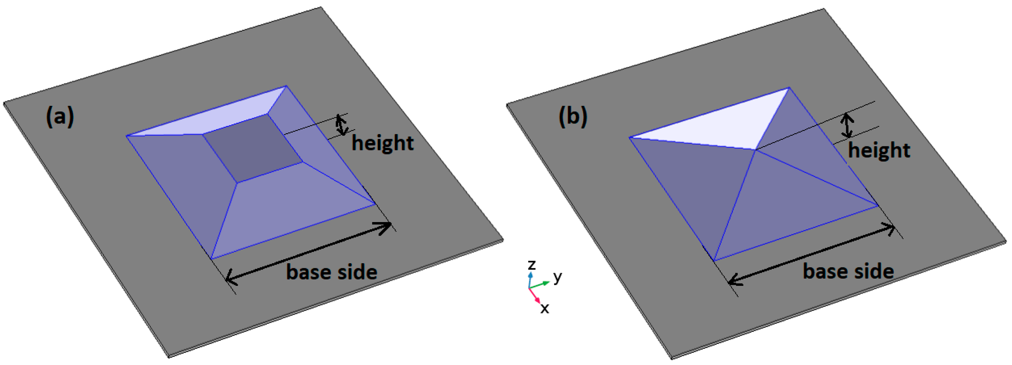
Furthermore, the QD is supposed to be formed by pure InAs material with truncated or full pyramidal shapes in accordance with structural reports [8,10]. A typical schematic presentation of the modeled QDs are given in Figure 2.
The key parameters allow tailoring of the carriers’ confined energies and, consequently, the interband transitions are the QD height and base length. In the case of the truncated pyramidal shape, the ratio between upper and base surfaces of the QD represents an additional degree of freedom that promotes a more effective matching of the theoretical emission energies to the experimental ones.
3. Results and Discussion
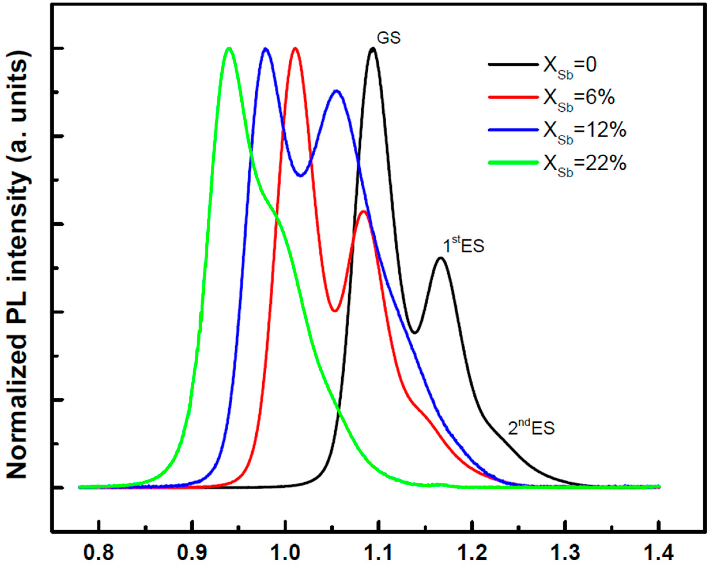
The 77 K PL spectra of the investigated samples (XSb = 0%, 6%, 12% and 22%), recorded with an excitation density of 160 W/cm2, is shown in Figure 3. Regardless of the Sb content in the CL, all the spectra show a multiple peaks feature arising from the state filling effects. Indeed, a ground state and two excited states emission peaks are present in each PL spectra. Additionally, the PL peaks energies get continuously red-shifted with increasing XSb, testifying that increasing XSb alters the QDs shape and size.
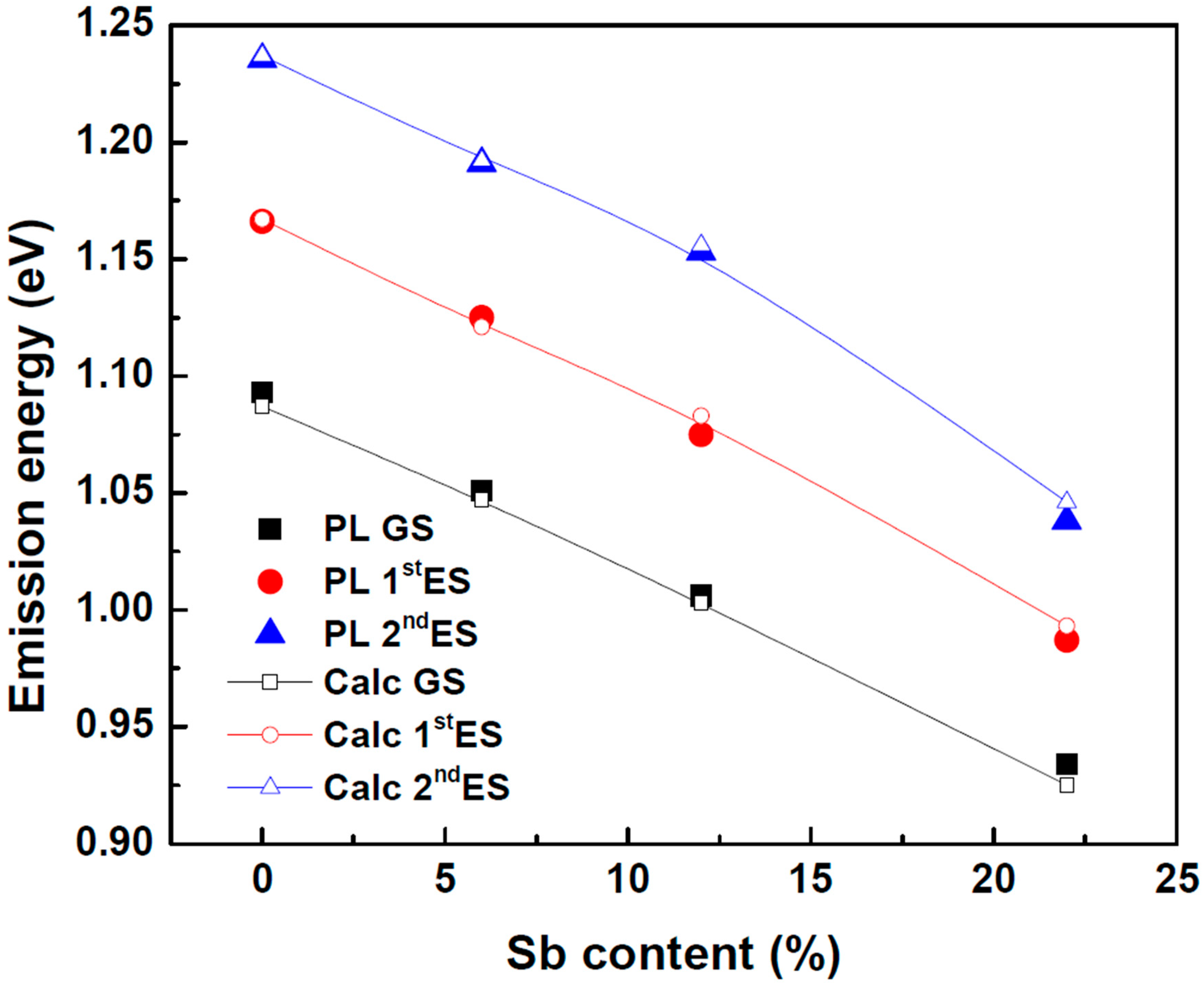
In order to estimate, numerically, the buried QDs shape and size for each sample, Equation (1) has been numerically solved for InAs QD capped with a GaAsSb layer, thereby yielding the electrons’ and holes’ energy states and corresponding wave functions for the XSb contents considered. The numerical procedure consists of tuning the QD size parameters (height and base length), allowing to tailor the carriers’ confined energy states until reaching the best correlation between theoretical and experimental emission energies [24]. The matching between the numerically driven interband transition energies corresponding to the ground- (GS), the first- (1st ES) and the second- (2nd ES) excited-states with those given experimentally by PL spectroscopy, permit an accurate estimation of the QD size and shape. For XSb = 22%, a full-pyramidal-shaped QD has been considered to match the theoretical emission energies with the experimental ones. However, for low Sb content ( XSb ≤ 12%), the PL emission energies could not be reproduced by using the same QD shape. Meanwhile, good agreement has been reached by considering a truncated-pyramidal-shaped QD. Furthermore, the upper to base surface ratio of the truncated-pyramidal-shaped dots is found to decrease from 70% down to 60% when the Sb content increases from 0% to 12%. The optimization process yields truncated-pyramid-shaped QDs for the low-Sb-content regime and full-pyramid-shaped dots for higher Sb content of the CL. The theoretical interband transition energies that give rise to the optimum dot shape and size are presented in Figure 4, together with the PL emission energies for each Sb content.
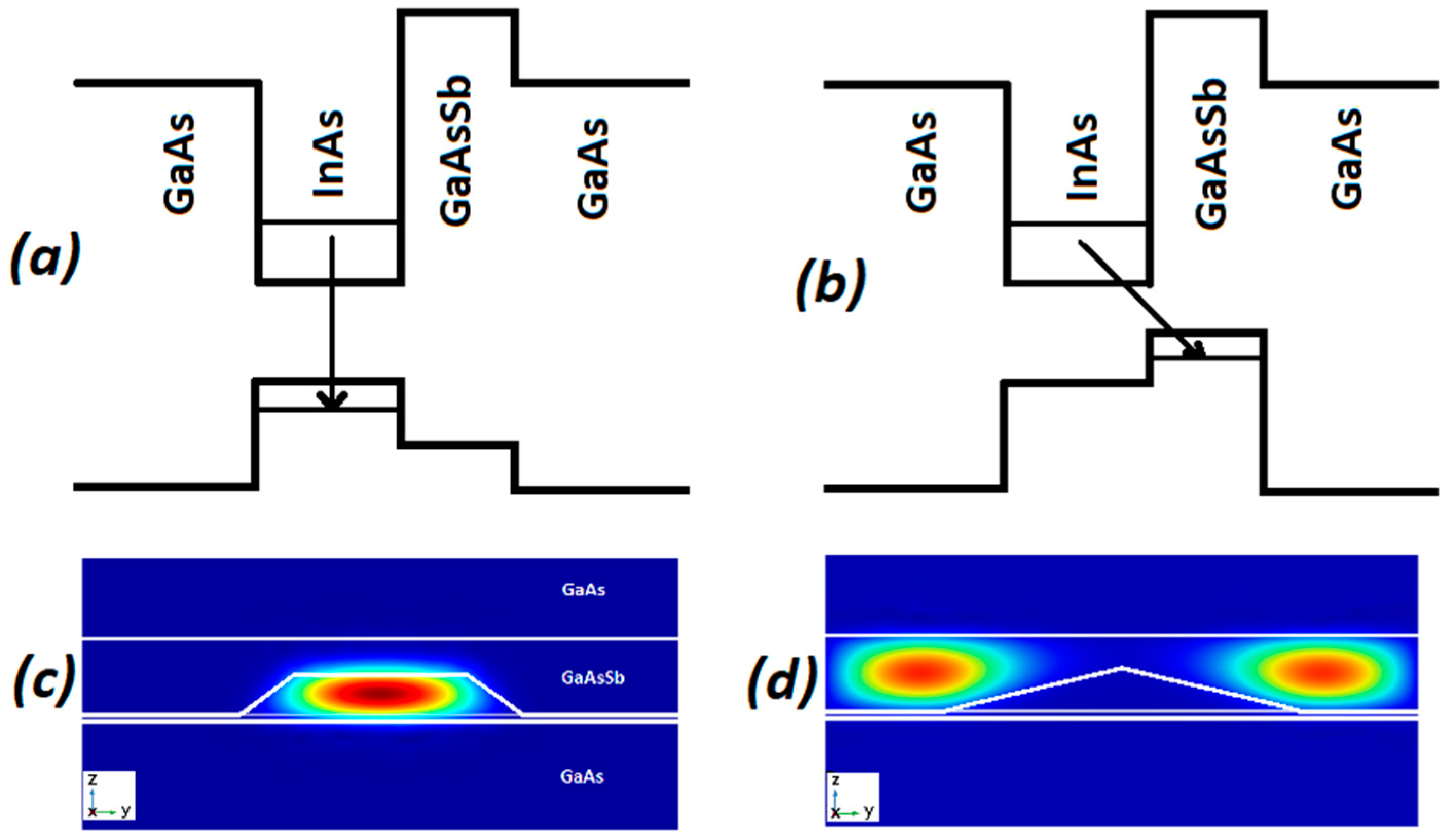
Furthermore, for the low Sb content (0%, 6%, and 12%), the InAs/GaAsSb band alignment is found to be type I. However, the Sb content of 22% shows type II band alignment. The transition between type I and type II band alignment has been found to occur around XSb = 14%, which is in good agreement with the literature [9,13]. The energy spacing between the successive interband transition energies is found to be almost constant (around 70 meV) for XSb below 12% (type I). However, for XSb = 22%, a reduction of the emission energy spacing by approximately 20 meV is observed and likely to be a direct consequence of the type II band alignment. Indeed, the transition energies involves different electron confined states to a single heavy-holes state in the quantum well, such as GaAsSb CL. A schematic band lineup, as well as typical ground-state heavy holes envelope wave function, are shown by the Figure 5, for XSb = 6% (type I) and XSb = 22% (type II).
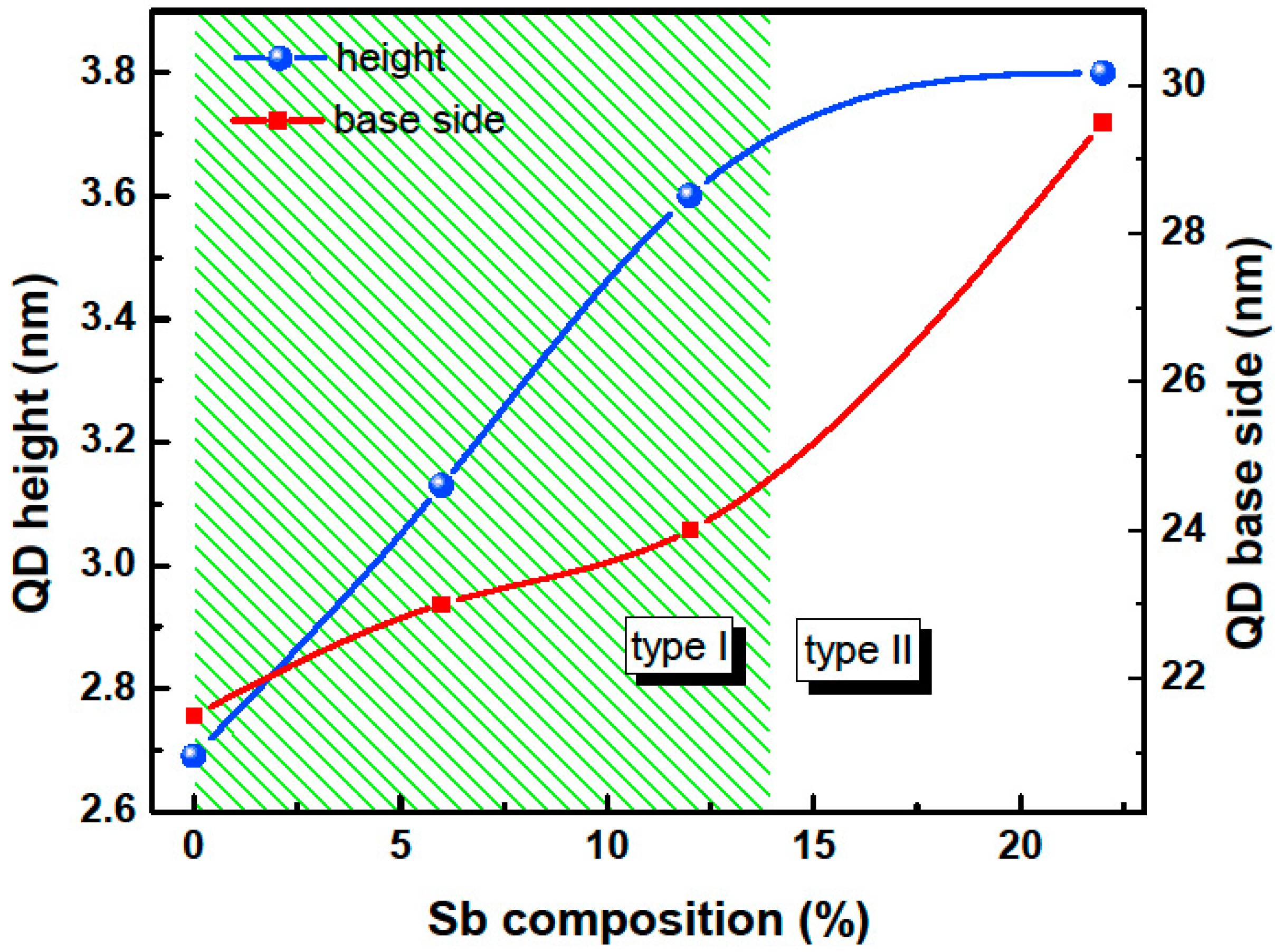
The evolution of the buried QD height and base side as a function of the CL Sb content is plotted in Figure 6. Both QD height and base length show a monotonic increase upon increasing the Sb content of the CL, indicating that the QD decomposition is progressively prohibited with increasing XSb.
Accordingly, the surfactant effect of the Sb atoms has been experimentally shown to limit the In segregation and the In-Ga intermixing during the initial stage of the QD capping [25]. In the present case, the enhancement of the QDs size upon increasing of the CL Sb content up to 12% is accompanied by a reduction of the truncated pyramid QDs’ upper surface. At an Sb content of 22%, the best modeling results are achieved for an entire pyramidal-shaped QD.
The QD height is linearly enhanced by approximately 1 nm when the CL Sb content increases by 12%. However, further increasing XSb by 10% (from 12% to 22%) results in an overall increase of the QD height by only 0.2 nm testifying a quasi-saturation of the QD height increase at this composition range. This behavior suggests the suppression of the QD dissolution in accordance with experimentally observed complete suppression for an Sb content of 14% [10].
The present results agree well with the cross-sectional scanning tunneling microscopy observed evolution of the QD size and shape as a function of the Sb content in the CL [10]. This testifies that the proposed method can be used to estimate the evolution of buried InAs/GaASb dots size and shape in a nondestructive and low-cost way.
It is worth noting that the adequate matching of multiple PL emission energies arising from the ground- and excited-states of QDs with a narrow size distribution constrains the modeled QD to a specific geometry. The uniqueness of the QD size and geometry that leads to the optimum matching effectively describes the realistic one. Meanwhile, the extracted dots’ size and shape are a rather representative assessment of the average size exhibited by the dominant dot population involved in the maximum PL intensity. Indeed, in view of the self-organized QD complexities, including the inevitable size and composition fluctuation, the accurate assessment of an average size and shape is highly requested for comprehensive studies and routine analysis of the experiments during the dots growth-optimization process.
4. Conclusions
The correlation between InAs QDs’ numerical simulation and PL experiments has revealed a strong dependence of the buried dots size and shape on the CL Sb content. This result confirms the role of the Sb atoms in reducing the QDs decomposition, leading to an enhanced dots’ height and base length upon increasing the Sb content. The QDs’ shape are found to follow a truncated pyramid in the low composition regime (less than 14%) and entire pyramidal shape for higher CL composition. The results are in agreement with a structural investigation reported in the literature that showed the suitability of the employed model for experimental routine studies aiming to optimize the desired QDs size for a specific application.
Author Contributions
Conceptualization and Formal analysis A.S. and B.I.; Writing-original draft K.A.; Investigation A.S. and K.A. Validation B.I. and N.A.M.; Supervision B.I.; Writing-review & editing B.I., A.S., N.A.M.
Funding
This research received no external funding.
Acknowledgments
The authors would like to thank the Deanship of Scientific Research at King Saud University for funding this work through the Research Group No: RG-1436-014.
Conflicts of Interest
The authors declare no conflict of interest.
References
- Liu, H.; Wang, T.; Jiang, Q.; Hogg, R.; Tutu, F.; Pozzi, F.; Seeds, A. Long-wavelength InAs/GaAs quantum-dot laser diode monolithically grown on Ge substrate. Nat. Photonics 2011, 5, 16–419. [Google Scholar] [CrossRef]
- Towe, E.; Pan, D. Semiconductor quantum-dot nanostructures: Their application in a new class of infrared photodetectors. IEEE J. Sel. Top. Quantum Electron. 2000, 6, 408–421. [Google Scholar] [CrossRef]
- Hatch, S.; Wu, J.; Sablon, K.; Lam, P.; Tang, M.; Jiang, Q.; Liu, H. InAs/GaAsSb quantum dot solar cells. Opt. Express 2014, 22, A679–A685. [Google Scholar] [CrossRef]
- Akahane, K.; Yamamoto, N.; Ohtani, N. Long-wavelength light emission from InAs quantum dots covered by GaAsSb grown on GaAs substrates. Phys. E 2004, 21, 295–299. [Google Scholar] [CrossRef]
- Ripalda, J.M.; Granados, D.; González, Y.; Sánchez, A.M.; Molina, S.I.; García, J.M. Room temperature emission at 1.6 μm from InGaAs quantum dots capped with GaAsSb. Appl. Phys. Lett. 2005, 87, 202108. [Google Scholar] [CrossRef]
- Liu, H.Y.; Steer, M.J.; Badcock, T.J.; Mowbray, D.J.; Skolnick, M.S.; Suarez, F.; Ng, J.S.; Hopkinson, M.; David, J.P.R. Room-temperature 1.6 μm light emission from InAs/GaAs quantum dots with a thin GaAsSb cap layer. J. Appl. Phys. 2006, 99, 046104. [Google Scholar] [CrossRef]
- Nasr, O.; Alouane, M.H.H.; Maaref, H.; Hassen, F.; Sfaxi, L.; Ilahi, B. Comprehensive investigation of optical and electronic properties of tunable InAs QDs optically active at O-band telecommunication window with (In) GaAs surrounding material. J. Lumin. 2014, 148, 243–248. [Google Scholar] [CrossRef]
- Ulloa, J.M.; Drouzas, I.W.D.; Koenraad, P.M.; Mowbray, D.J.; Steer, M.J.; Liu, H.Y.; Hopkinson, M. Suppression of InAs/GaAs quantum dot decomposition by the incorporation of a GaAsSb capping layer. Appl. Phys. Lett. 2007, 90, 213105. [Google Scholar] [CrossRef]
- Ban, K.-Y.; Kuciauskas, D.; Bremner, S.P.; Honsberg, C.B. Observation of band alignment transition in InAs/GaAsSb quantum dots by photoluminescence. J. Appl. Phys. 2012, 111, 104302. [Google Scholar] [CrossRef]
- Ulloa, J.M.; Gargallo-Caballero, R.; Bozkurt, M.; Del Moral, M.; Guzmán, A.; Koenraad, P.M.; Hierro, A. GaAsSb-capped InAs quantum dots: from enlarged quantum dot height to alloy fluctuations. Phys. Rev. B 2010, 81, 165305. [Google Scholar] [CrossRef]
- Zhang, Z.; Huang, Y.; Reece, P.J.; Bremner, S.P. Influence of GaAsSb structural properties on the optical properties of InAs/GaAsSb quantum dots. Phys. E 2017, 94, 7–14. [Google Scholar] [CrossRef]
- Liu, H.Y.; Steer, M.J. Long-wavelength light emission and lasing from InAs∕GaAs quantum dots covered by a GaAsSb strain-reducing layer. Appl. Phys. 2005, 86, 143108. [Google Scholar] [CrossRef]
- Hospodková, A.; Zíková, M.; Pangrác, J.; Oswald, J.; Kubištová, J.; Kuldová, K.; Hazdra, P.; Hulicius, E. Type I–type II band alignment of a GaAsSb/InAs/GaAs quantum dot heterostructure influenced by dot size and strain-reducing layer composition. J. Phys. D Appl. Phys. 2013, 46, 095103. [Google Scholar] [CrossRef]
- Utrilla, A.D.; Reyes, D.F.; Llorens, J.M.; Artacho, I.; Ben, T.; González, D.; Gačević, Ž.; Kurtz, A.; Guzman, A.; Hierro, A.; et al. Thin GaAsSb capping layers for improved performance of InAs/GaAs quantum dot solar cells. Sol. Energy Mater. Sol. Cells 2017, 159, 282–289. [Google Scholar] [CrossRef]
- Krishna, J.S.; Panda, D.; Chakrabarti, S. Impact of Sb Composition on Strain Profile of GaAs1−xSbx Capped InAs Quantum Dots. IEEE Trans. Nanotechnol. 2019, 18, 234–239. [Google Scholar] [CrossRef]
- Guo, Y.; Liu, Y.; Liang, B.; Wang, Y.; Guo, Q.; Wang, S.; Fu, G.; Mazur, Y.I.; Ware, M.E.; Salamo, G.J. Carrier dynamics of InAs quantum dots with GaAs1−xSbx barrier layers. Appl. Phys. Lett. 2017, 111, 191105. [Google Scholar] [CrossRef]
- Salhi, A.; Alshaibani, S.; Alhamdan, M.; Albrithen, H.; Alyamani, A.; El-Desouki, M. Effects of Sb incorporation in GaAsSb-capping layer on the optical properties of InAs/GaAs QDs grown by Molecular Beam Epitaxy. Superlattices Microstruct. 2017, 101, 138–143. [Google Scholar] [CrossRef]
- Califano, M.; Harrison, P. Presentation and experimental validation of a single-band, constant-potential model for self-assembled InAs/GaAs quantum dots. Phys. Rev. B 2000, 61, 10959. [Google Scholar] [CrossRef]
- Ngo, C.Y.; Yoon, S.F.; Fan, W.J. Effects of size and shape on electronic states of quantum dots. Phys. Rev. B 2006, 74, 245331. [Google Scholar] [CrossRef]
- Salhi, A.; Alshaibani, S.; Ilahi, B.; Alhamdan, M.; Alyamani, A.; Albrithen, H.; El-Desouki, M. Tailoring the optical properties of InAs/GaAs quantum dots by means of GaAsSb, InGaAs and InGaAsSb strain reducing layers. J. Alloys Compd. 2017, 714, 331–337. [Google Scholar] [CrossRef]
- Vurgaftman, I.; Meyer, J.R. Band parameters for III–V compound semiconductors and their alloys. J. Appl. Phys. 2001, 89, 5815–5875. [Google Scholar] [CrossRef]
- Van de Walle, C.G. Band lineups and deformation potentials in the model-solid theory. Phys. Rev. B 1989, 39, 1871. [Google Scholar] [CrossRef]
- Liu, G.; Chuang, S.-L. Optical gain of strained GaAsSb/GaAs quantum-well lasers: A self-consistent approach. J. Appl. Phys. 2000, 88, 5554–5561. [Google Scholar] [CrossRef]
- Ilahi, B.; Souaf, M.; Baira, M.; Alrashdi, J.; Sfaxi, L.; Alhazaa, A.; Maaref, H. Evolution of InAs/GaAs QDs Size with the Growth Rate: A Numerical Investigation. J. Nanomater. 2015, 16, 287. [Google Scholar] [CrossRef]
- Gong, Q.; Offermans, P.; Nötzel, R.; Koenraad, P.M.; Wolter, J.H. Capping process of InAs∕GaAs quantum dots studied by cross-sectional scanning tunneling microscopy. Appl. Phys. Lett. 2004, 85, 5697. [Google Scholar] [CrossRef]
Figure 1.
Schematic presentation of the GaAsSb-capped InAs QDs grown by molecular beam epitaxy.

Figure 2.
Schematic presentation of modeled QD geometry: (a) truncated pyramid and (b) pyramid.

Figure 3.
PL spectra at 77 K with an excitation power of 160 W/cm2, from the InAs QDs samples with different Sb contents observed in the CL.
Figure 3.
PL spectra at 77 K with an excitation power of 160 W/cm2, from the InAs QDs samples with different Sb contents observed in the CL.

Figure 4.
Interband transition energies from the ground states and the first two excited states: the filled symbols represent the experimental data and the line and symbols represent the best matching between the experimental and theoretical values obtained by tailoring the QDs’ shape and size.
Figure 4.
Interband transition energies from the ground states and the first two excited states: the filled symbols represent the experimental data and the line and symbols represent the best matching between the experimental and theoretical values obtained by tailoring the QDs’ shape and size.

Figure 5.
Schematic band lineup (a): Type I and (b) type II. (c) and (d) are, respectively, the cross-sectional heavy-hole envelope wave function for XSb = 6% (truncated pyramidal shape/type I) and XSb = 22% (full pyramidal shape/type II).
Figure 5.
Schematic band lineup (a): Type I and (b) type II. (c) and (d) are, respectively, the cross-sectional heavy-hole envelope wave function for XSb = 6% (truncated pyramidal shape/type I) and XSb = 22% (full pyramidal shape/type II).

Figure 6.
Numerically driven QD height (filled blue circles) and base side (filled red squares) as a function of the Sb content in the CL. The green pattern delimits the low Sb content CL, giving rise to a type I band alignment.
Figure 6.
Numerically driven QD height (filled blue circles) and base side (filled red squares) as a function of the Sb content in the CL. The green pattern delimits the low Sb content CL, giving rise to a type I band alignment.

© 2019 by the authors. Licensee MDPI, Basel, Switzerland. This article is an open access article distributed under the terms and conditions of the Creative Commons Attribution (CC BY) license (http://creativecommons.org/licenses/by/4.0/).
Share and Cite
MDPI and ACS Style
Alshehri, K.; Salhi, A.; Ahamad Madhar, N.; Ilahi, B. Size and Shape Evolution of GaAsSb-Capped InAs/GaAs Quantum Dots: Dependence on the Sb Content. Crystals 2019, 9, 530. https://0-doi-org.brum.beds.ac.uk/10.3390/cryst9100530
AMA Style
Alshehri K, Salhi A, Ahamad Madhar N, Ilahi B. Size and Shape Evolution of GaAsSb-Capped InAs/GaAs Quantum Dots: Dependence on the Sb Content. Crystals. 2019; 9(10):530. https://0-doi-org.brum.beds.ac.uk/10.3390/cryst9100530
Chicago/Turabian StyleAlshehri, Khairiah, Abdelmajid Salhi, Niyaz Ahamad Madhar, and Bouraoui Ilahi. 2019. "Size and Shape Evolution of GaAsSb-Capped InAs/GaAs Quantum Dots: Dependence on the Sb Content" Crystals 9, no. 10: 530. https://0-doi-org.brum.beds.ac.uk/10.3390/cryst9100530
Note that from the first issue of 2016, this journal uses article numbers instead of page numbers. See further details here.