LED as Transmitter and Receiver of Light: A Simple Tool to Demonstration Photoelectric Effect


1
Dipartimento di Matematica e Fisica, Università degli Studi “Roma Tre”, 00154 Rome Italy
2
Dipartimento di Scienze, Università degli Studi “Roma Tre”, 00154 Roma, Italy
*
Author to whom correspondence should be addressed.
Crystals 2019, 9(10), 531; https://0-doi-org.brum.beds.ac.uk/10.3390/cryst9100531
Submission received: 5 September 2019
/
Revised: 23 September 2019
/
Accepted: 9 October 2019
/
Published: 15 October 2019
(This article belongs to the Special Issue Recent Advances in Light-Emitting Diodes (LEDs))
Abstract
:The experimental observations of the photoelectric effect show the properties of quantum mechanics of the electromagnetic field. For this reason, this important effect is commonly used as an introductory topic for the study of quantum physics. The “classical” demonstration of the photoelectric effect is very incisive; unfortunately, the experimental apparatus is not cheap and easy to realize. The typical use of LEDs is as light emitters, but they can be used even as photosensors and, in this case, they are sensitive to wavelengths equal to or shorter than the predominant wavelength it emits. Furthermore, a LED used as detector is sensitive to wavelengths equal to or shorter than the predominant wavelength it emits. This ability of LEDs offers the possibility of developing a simple tool able to demonstrate the photoelectric effect. This paper describes the realization of an economic, simple, easy and safe system to use for the experimental demonstration of the photoelectric effect, based on the LED to LED structure. The paper has educational purposes, oriented towards laboratory teaching activities.
1. Introduction
The teaching on quantum mechanics and new technologies plays an important role in the academic community [1,2,3]. In particular, the role that quantum mechanics acts as a reference theory for the microscopic description of reality is generally recognized [4]. In school education the introduction of the corpuscular nature of light makes it possible to understand the performing of many commonly used technological objects. Richard Feynman emphasized the importance of this: “I want to emphasize that light comes in this form—particles. It is very important to know that light behaves like particles, especially for those of you who have gone to school, where you were probably told something about light behaving like waves” [5].
The photoelectric effect is generally used as the introductory topic for the study of quantum physics [6,7,8,9,10]. The main aspect of photoelectric effect is that showed that the kinetic energy of photoelectrons depends linearly on the incident light frequency but is independent of its intensity. This explanation is central in our understanding of light and it is demonstrated experimentally in many introductory physics courses. The classic apparatus for these demonstrations includes a phototube, a variable voltage source, current and voltage meters and a light source (a mercury lamp or an incandescent bulb) capable of generating several narrow bandwidths of light [11].
One drawback, to using “classical apparatus”, in student laboratory, is the light source. The incandescent source has inherent disadvantage of low intensity, mainly at the shorter wavelengths, while the mercury source can be dangerous (high temperature, ultraviolet output, mercury vapor). To solve these problems, Light Emitting Diodes (LEDs) can be used as light source [12,13].
LED technology is widely present in our everyday life, like car headlights, TV and monitor technology, illumination systems for domestic and professional use [14,15,16,17,18]. In 2014 Isamu Akasaki, Hiroshi Amano e Shuji Nakamura received the Nobel Prize in Physics for the development of a blue light LED [19,20].
Compared to traditional light sources, LEDs are devices with low-cost, very small dimensions, high reliability, low heat generation, longer life, great availability in colors of the emitted light. The ability of LEDs to emit light at various wavelengths is well-known. Less familiar is the ability of LEDs to be used as selective light sensors. Indeed, the working principle of LED in the photodetector mode is like that of a conventional photodiode [21,22,23,24,25,26].
The aim of this paper is to realize an economic, simple, easy and safe system to use for the experimental demonstration of the photoelectric effect. Tool also able to offer the possibility of experimenting with the use of LED not only as a light emitter but also as wavelength selective sensor.
The remaining of this paper is organized as follows. A brief description of the basic properties of the photoelectric effect are described in Section 2. Work’s principle of LEDs is given in Section 3. In Section 4, we present the realized tool. Section 5 contains some notes on the possibility of making wireless commissions using LED to LED systems. Finally, conclusions are drawn in Section 6.
2. Basic Properties of the Photoelectric Effect
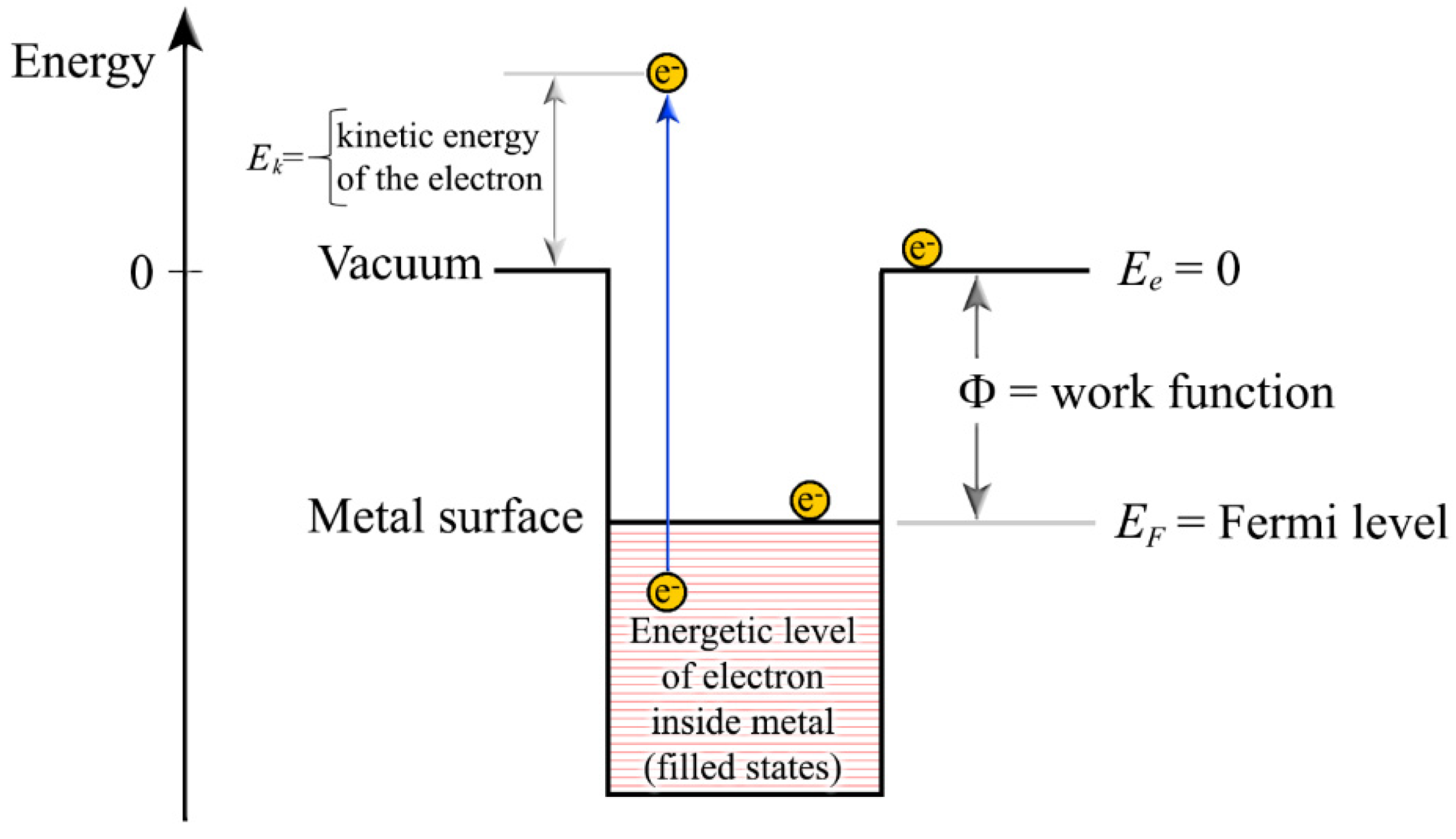
The photoelectric effect occurs when a light beam is incident on a metal surface causing electrons to be ejected from the surface. One or more of the outer electrons of each metal atom is free to wander in the field of the ion cores, effectively binding the metal together. In fact, the metal crystal may be viewed as a periodic arrangement of positively charged ion (the positively charged nuclei and non-valence electrons). The positive ions create a potential well, as shown in the Figure 1, and the free electrons occupy the states of lowest energy.
In a metallic crystal, the electrons fill the available states up to a certain energy called Fermi level. If an electron is given enough energy, it may be separated completely from the metal and wander freely outside of it. The amount of energy needed to “eject” the electron from the metal is called the work function. In other words, the work function (Φ) is the amount of work that must be done on the electron (located in the potential well) to make it free. The shallower the well (i.e., the lower the work function “Φ”), less is the energy required to cause the emission of the electron. Since different metal atoms have different positive ions disposition, it is logical to assume that the work function (Φ) depends on the metal.
The photoelectric effect can be expressed by
In Equation (1). Ek(max) is the maximum kinetic energy of the electrons ejected, Elight is the energy of the electromagnetic radiation incident on a metal surface, and Φ is the metal work function.
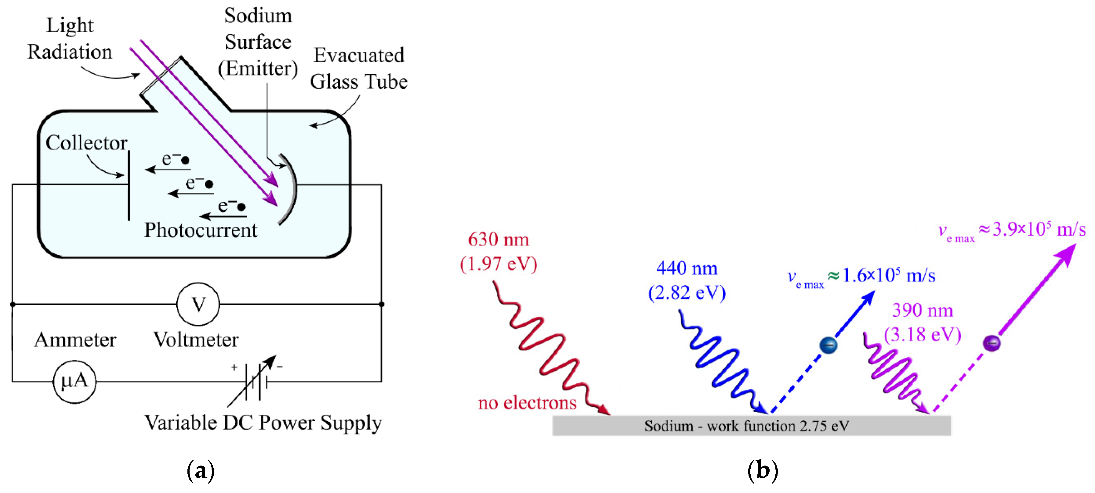
The basic experimental set up which explains photoelectric effect is as given in Figure 2a. Typical setup consists of a metal plate on which light shines. This plate is called the emitter (sodium in figure). Across from the emitter is a plate called collector. The emitter is connected to the negative terminal of a variable dc voltage source and the collector is connected to the positive terminal.
Light strikes the emitter, which causes photoelectric electrons to be emitted. The electrons are attracted to the positively charged collector and a photocurrent is established. Generally, the radiation sent on the emitter comes from a mercury discharge tube that produces light at the characteristic frequencies of the mercury spectrum. The individual mercury lines can be selected by appropriate optical filters.
According to the classical wave theory of light, the magnitude of the electric field vector of a light wave goes like the square root of the intensity of the light, . Thus, as the intensity increases, the electric field magnitude increases. Since the force on an electron is proportional to the electric field vector, it is expected that the kinetic energy of a photoelectron should increase with the intensity of incident light. Furthermore, the photoemission should occur at all wavelengths of incident light, if the incident radiation has enough intensity.
In contrast, the experiment showed that the maximum speed of photoelectrons does not depend on intensity; the light intensity affects only the number of ejected electrons and not their kinetic energies. In particular, the maximum of kinetic energy of the emitted electron be contingent on the type of emitter used and, on the color (wavelength) of the incident light radiation.
Einstein [9], to resolve the contradictions between the classical theory of electromagnetic waves and the experimental results of the photoelectric effect, the energy carried by each particle of light (called quanta or photon) is dependent on the light’s frequency (). In other words, the photons of a light beam have a characteristic energy proportional to the frequency of the light. That is:
Einstein theorized that the light is bundled up into photons. When a photon falls on the surface of a metal, all the energy of the photon can be transferred to the electron. A part of this energy is used to remove the electron from the metal atom’s grasp () and the rest is given to the ejected electron as kinetic energy. Electrons emitted from underneath the metal surface lose some of the kinetic energy during the collision. But the surface electrons carry all the kinetic energy imparted by the photon and have the maximum kinetic energy.
We must also consider that the electrons can absorb energy from photons according to the rule “all or nothing” principle. All the energy from one photon must be absorbed and used to liberate one electron from atomic binding, or else the energy is re-emitted.
With Einstein’s interpretation, Equation (1) becomes:
where c is the light speed and λ le wavelength of the incident light.
The Equation (3) shows that, given the work function (Φ) (chosen the metal on which to make the light engrave), there exists a certain minimum frequency of incident radiation () below which no photoelectrons are emitted; this represents one of the evidences that the energy carried by light is quantized.
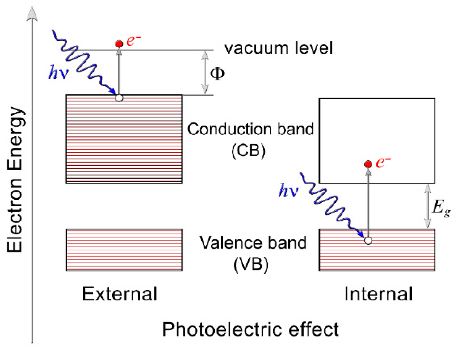
What described above represents the external photoelectric effect. In the external photoelectric effect, the electrons present on the surface of a metal receive energy from the absorption of a photon. If the energy absorbed is greater than the binding energy (work function Φ), they acquire kinetic energy which allows them to be able to leave the metal.
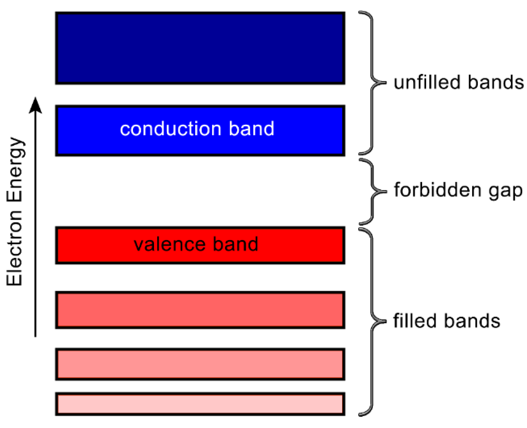
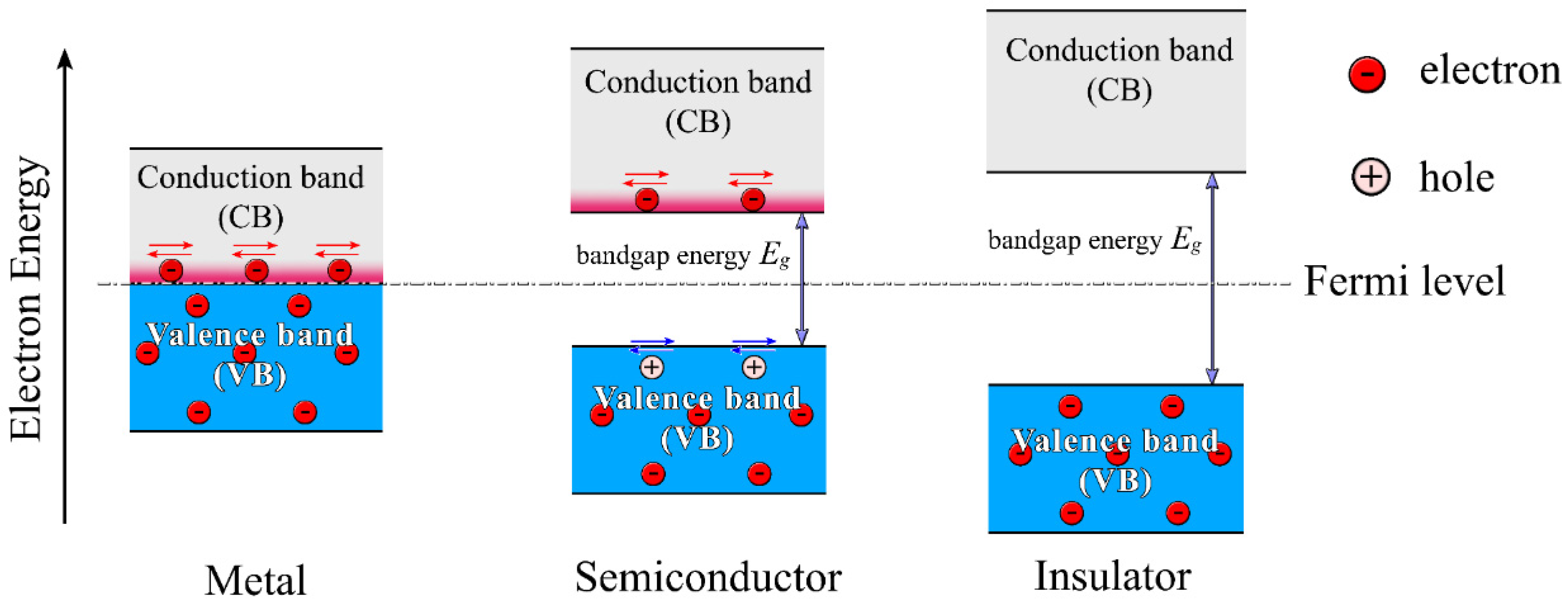
Electrons in an isolated atom can only have discrete energy levels, but when atoms are together as in crystalline solids, these energy levels will split into many separated. Because the levels are so closely separated, they may be treated as a continuous band of allowed energy states. Therefore, in solid-state physics the electronic band structure of a crystalline solids describes the energy states that an electron is allowed or forbidden to be in. Most of the states with low energy (closer to the nucleus) are occupied, up to a particular band; usually, the highest filled band is called Valence Band (VB), whereas the lowest empty band is termed Conduction Band (CB) (see Figure 3) [29].
In general, band structures are complex. It is possible to find different bands that are not separated by energy gaps but can overlap instead. Semiconductors and insulators are distinguished from metals by the population of electrons in each band. In each metal there is no band gap between their valence and conduction bands. In the next section, more details on the energy bands formation will be given.
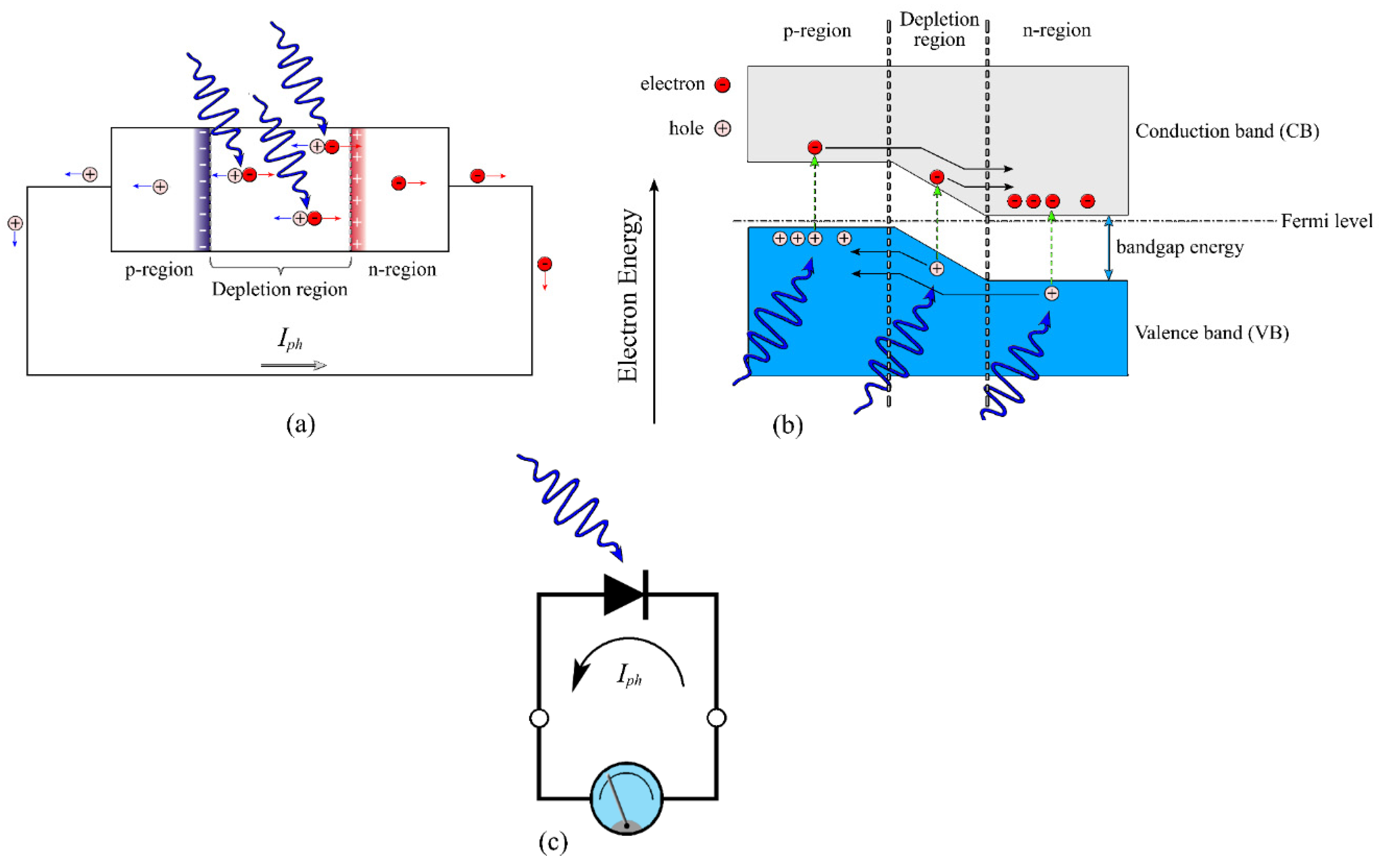
Due to the band structure of the energy levels of the electrons in a crystalline solid, there is the possibility of observing the internal photoelectric effect. This effect occurs when the electrons get energy from the absorption of a photon. Due to this increase in energy, the electron is promoted from the valence band into the conduction band. It is not ejected from the material surface but is internally able to flow forming a photo-current or is able to modify the material conductivity.
Figure 4 shows schematically the difference between the external and the internal photoelectric effect.
3. Photoelectric Effect in LED
The experimental apparatus of Figure 2a is well suitable for quantitative study of the photoelectric effect, but the apparatus is too complex for demonstration in undergraduate classrooms.
To realize an economic, simple, easy and safe system to use for the experimental demonstration of the photoelectric effect, it is possible to use a LEDs-LEDs system. In other words, a series of LEDs is used to vary the wavelength of the incident radiation. Additionally, other LEDS are used as materials on which the light is sent (LEDs used as selective wavelength sensors).
Compared to the “classic” apparatus, this new system replaces the mercury lamp, combined with wavelength selection filters, with LEDs [12,30]. Furthermore, other LEDs are used as light receivers; they replace the metals on which electromagnetic radiation is sent [31,32,33,34].
3.1. Semiconductor LEDs, How Do They Work?
The working principle of the Light Emitting Diode (LED) is based on the quantum theory.
A particle, as can be considered the photon and the electron according to Einstein’s special relativity theory [35,36], has energy:
Here: is energy; is rest mass; c is vacuum speed of light; p is momentum. Therefore, for photon (E = h⋅ν) we have:
Introducing the wave number we can write:
In Equation (5), ħ represent the Dirac constant .
Atoms of solid-state materials have a sufficiently strong interaction that they cannot be treated as individual entities. Valence electrons are not attached (bound) to individual atoms; rather, they belong to the system of atoms.
The band structure of a crystalline solid is the relationship between the energy E of the electrons of the solid and the wave vector k (i.e., momentum) [37]. It comes from the Schrödinger equation (Equation (7)) of an approximate one-electron problem in a periodic potential U(r) with the periodicity of the crystal lattice:
In Equation (7), ħ represent the Dirac constant , r is a vector of the direct lattice, the wave function describing the given electron, and m its energy and mass respectively. In the case of a periodic crystal, the Bloch’s theorem [38,39,40] gives the form of the solutions of the Schrödinger equation. There are domains of energy where no solution exists. These domains are forbidden electrons cannot have energies with values belonging to these regions. Above and below this energy gap are permitted energy regions called bands. In each solid material there are two important bands of energy
Valence Band (VB): the range of permissible energy values that are the highest energies an electron can have and still be associated with a particular atom of a solid material.
Conduction Band (CB): the range of permissible energy values which an electron in a solid material can have that allows the electron to dissociate from a particular atom and become a free charge carrier in the material.
The energy difference between the highest occupied energy state of the valence band and the lowest unoccupied state of the conduction band is called the band gap is equal to:
In Equation (8) is the bandgap energy, one the most important parameters in semiconductor physics. In metals one energy bands are partially filled; no bandgap energy between Valence and conductive band is present. The energy level separating the occupied and unoccupied states is known as the Fermi level. Since there are available states immediately above the Fermi surface, it requires an infinitesimal amount of energy to excite an electron from one of the highest occupied states to one of the lowest unoccupied states. Depending on the magnitude of the band gap energy, different types of conductors are obtained. Metals, semiconductors and insulators are distinguished from each others by their electronic band structures. Their band structures are shown in the Figure 5.
If the band gap is sufficiently small external excitations, such as light, can enable the “jump” of an electron from the valence band to the conduction band. The energy of this electron increases by a value equal to Eg. Therefore, the minimum energy of the photon (hν) to cause this jump must be at least equal to Eg (energy conservation ⇒ hν > Eg). When an electron jumps the gap from the valence band, it creates a vacancy or hole in the valence band of the atom (i.e., it is devoid of an electron normally there). A hole, as one might imagine, is a positive charge relatively speaking, since it is the absence of a negative charge that would normally be there to give a net charge of zero. The process results in the production of an electron hole pair (see Figure 6a).
The light-emission process in a semiconductor is quite simple: when there is an electron in the conduction band and an empty state in the valence band, the conduction-band electron can relax to fill the empty state in the valence band, the energy difference (i.e., the band gap ) being released as an emitted photon (see Figure 6b). In other words, the electron and the hole recombine to emit a photon with energy approximately equal to the bandgap energy :
In order to increase the photon flux there must be many electrons in the conduction band (or holes in the valence band). In other words, the semiconductor must be “conductive” [42].
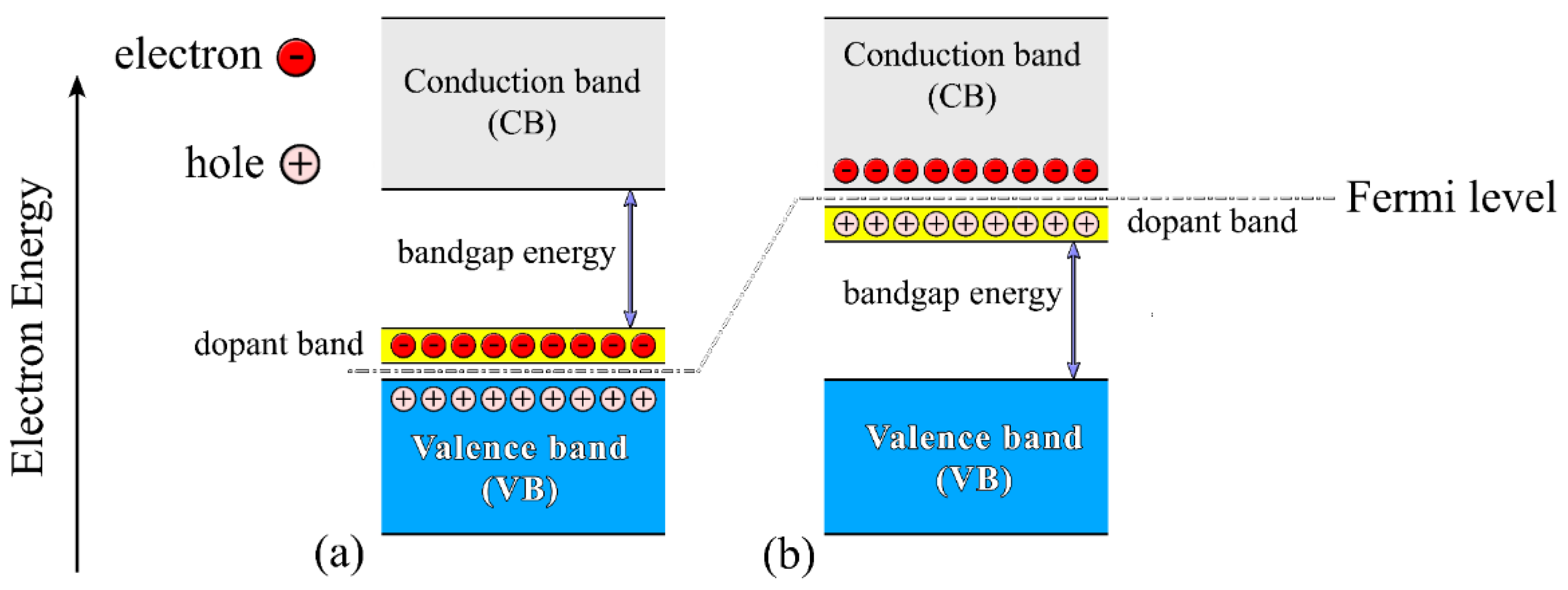
The semiconductors can be made “more” conductive either by putting extra electrons into the conduction band or by removing electrons from the valence band; this can be manufactured through the doping. Doping is the process of introducing new energy levels into the band gap. Doping can be affected by substituting a foreign element into the semiconductor lattice. Two types of doping can be distinguished, n-type and p-type. In n-type doping, occupied donor levels are created very near the conduction band edge. Likewise, p-type doping corresponds to the formation of empty acceptor levels near the valence band edge. The acceptor levels trap electrons from the valence band, creating positive charges as carriers. For n-type dopants, the energy band is very close to the bottom of the intrinsic conduction band, and room temperature provides enough energy to promote electrons from the dopant to conduction band and improves conductivity (Figure 7) by flowing through the partially filled bands. The same is true for p-type dopant materials except that the dopant energy level is empty and very close to the top of the intrinsic valence band allowing the valence electrons to be promoted to the dopant band and improve conductivity. Un-doped semiconductors are called intrinsic semiconductors. When a semiconductor is doped with impurities, it becomes extrinsic.
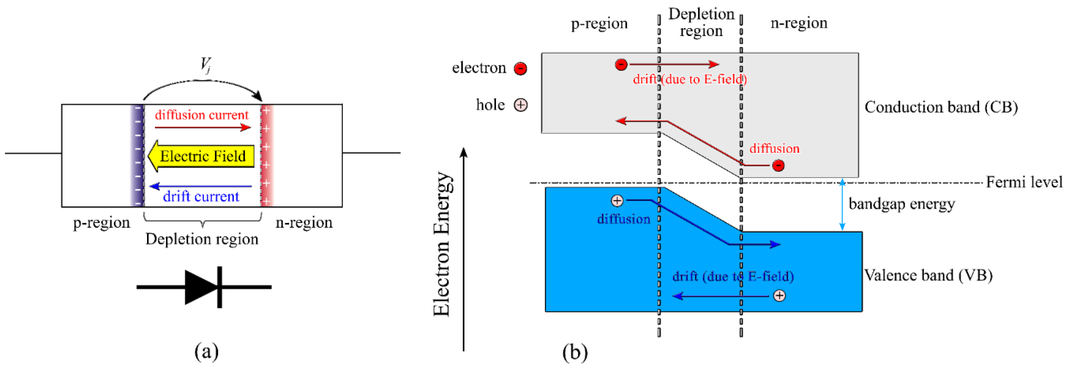
When p- and n-type semiconductors are brought into contact, a p-n junction (or diode) is formed. Once the p-n junction is first formed, mobile carriers (electron in n-region e hole in p-region) diffuse across the junction (due to the concentration gradients). Holes diffuse from the p-region to the n-region, leaving behind negatively charged immobile acceptor ions. Electrons diffuse from the n-region to the p-region, leaving behind positively charged immobile donor ions. A region depleted of mobile carriers is formed at the junction. The space charge due to immobile ions in the depletion region establishes a diffusion potential is generated (see Figure 8).
Excess negative charge forms in the p-region of the junction, and excess positive charge forms in the n-region of the junction, a barrier that effectively prevents more carriers from moving across the junction. The diffusion potential prevents more carriers from moving across the junction. In chemical equilibrium (no external bias) the Fermi’s level, is a constant across the junction. In turn, the energies of the conduction and valence bands for each of the materials (p and n type) will be moved, with the levels of the n-type material falling. A contact potential (Vj) develops, between the two materials, a voltage that is required to be placed across the junction to make electrons jump the band gap and allow current to flow. This is the bias voltage of the diode.
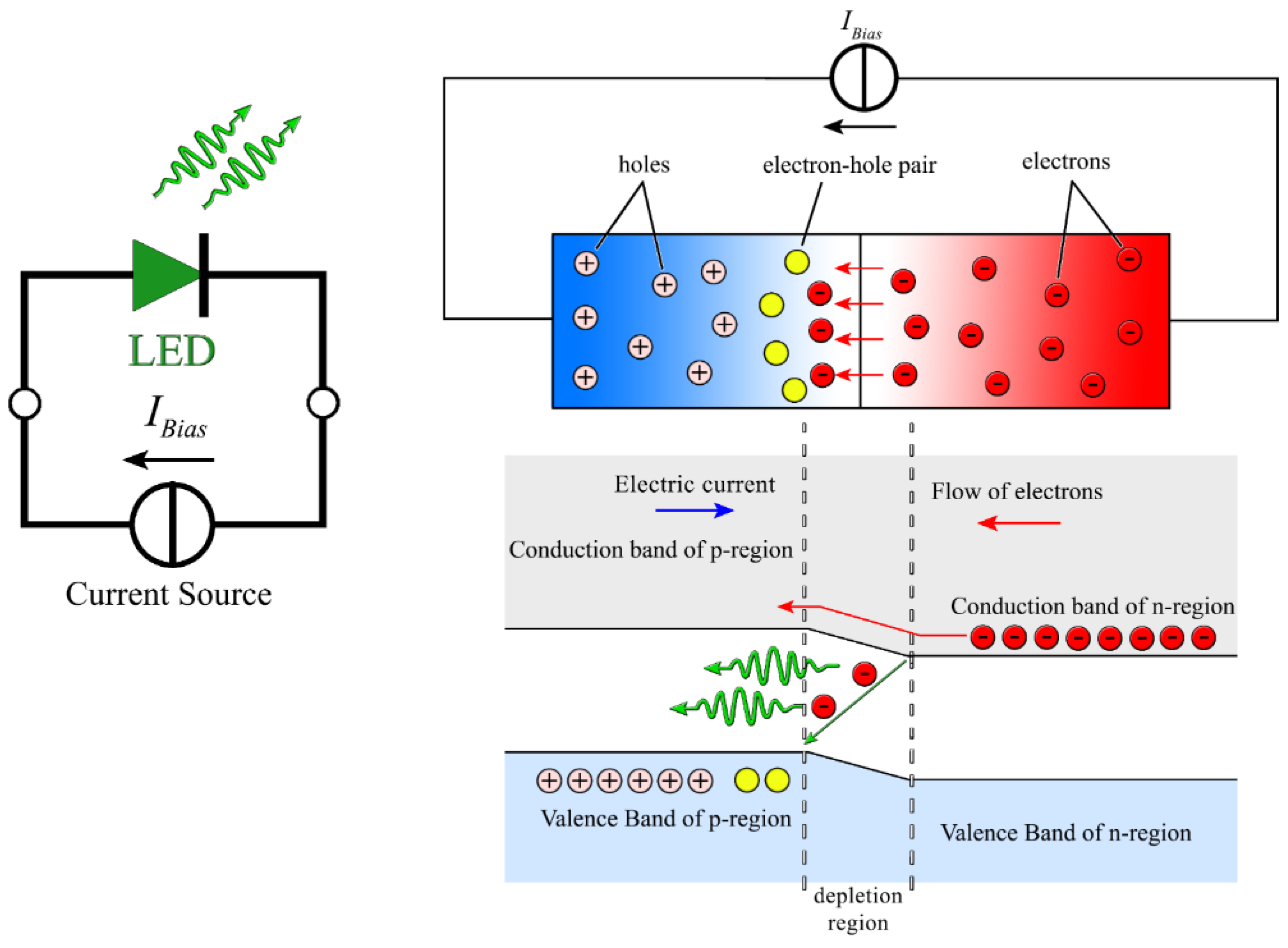
When the diode is forward biased, meaning that a potential large enough to overcome the contact potential of the junction is applied, electrons are supplied to the n-type material and holes to the p-type material (i.e., current flow through the p-n junction). To maintain electrical equilibrium, the excess injected carriers are removed by recombination of electron hole pairs in which electrons in the conduction band fall to the valence band, the result being the emission of a photon (in the case of an LED) or the production of heat by a non-radiative process (in most diodes used for signal applications). Figure 9 shows the flow of electrons and holes across the junction in a biased diode. There are many varieties of extrinsic semiconductor materials available for LEDs to create a specific color of light.
The main semiconductor materials used to manufacture LEDs are [43]:
- ▪
- Aluminum gallium arsenide (AlGaAs): infrared and red;
- ▪
- Gallium phosphide (GaP): yellow and green;
- ▪
- Aluminum gallium indium phosphide (AlGaInP): red, orange and yellow;
- ▪
- Indium gallium nitride (InGaN): green, blue and ultraviolet.
3.2. LEDs as Light Sensors
In addition to emitting light, an LED can be used as a photodiode light sensor/detector. This capability may be used in a variety of applications including ambient light level sensor and bidirectional communications. As a photodiode, an LED is sensitive to wavelengths equal to or shorter than the predominant wavelength it emits.
When photons with energy greater than bandgap fall on the depletion region of LED, they are absorbed, and electron-hole pairs are created (see Figure 10a). The electric field across the region pulls them apart causing a tiny current to flow. The more photons (light) the more the current adds up and so you have a current that is proportional to the light falling on the diode, this is called a photo current (see Figure 10b,c). As already mentioned, the phenomenon occurs only if the energy of the incident photons is greater than the energy gap of the semiconductor with which the LED is made (internal photoelectric effect). Therefore, using light with different wavelengths it is possible to verify this important effect.
4. Apparatus
In this work, we have implemented a simple tool, based on an LED-LED structure, suitable for demonstrating the internal photoelectric effect in a simple and economical way.
A diagram showing in schematic the various components of the implement apparatus is in Figure 11. The system is realized with two distinct functional sections: (a) piloting of the LED used as a light transmitter; (b) LEDs used as light receivers.
The realized apparatus is shown in Figure 12. The system is designed to be able to use different LEDs as light emitters. Two insulated sockets allow you to connect the LED of interest to the instrument.
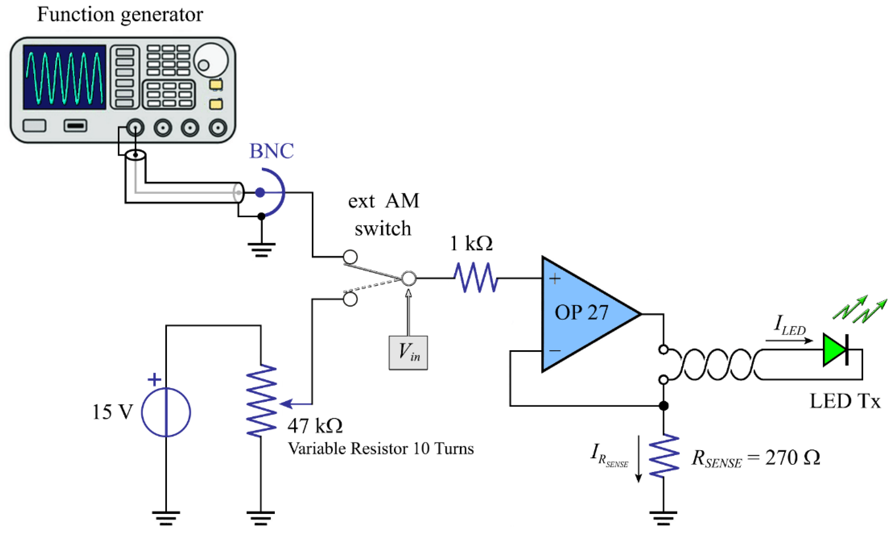
In the realized system, the section used to control the LED used as light transmitter is being implemented according the circuit shown in the Figure 13.
The circuit shown in Figure 13 drivers the LED Tx, used as a light source, with current supply. The key to the circuit’s operation is in placing a current sensing resistor (in our circuit RSENSE = 270 Ω) in the op amp (OP 27) feedback loop. The current delivered to the LED Tx is
The used circuit works on two simple principles (we remember that the voltages at the two inputs are the same and no current flows into the op amp’s input terminals [44]).
- The op amp adjusts its output to bring its negative input equal to the positive input. This means that tension across the RSENSE it is equal at the input voltage Vin.
- A simple application of Ohms law now tells you the current in RSENSE:the same current that is developed through RSENSE must also flow through the LED.
The emitted light of the LED is directly proportional to the current that passes through them. For this reason, the possibility to modify the intensity of the emitted light is a very important test case allows showing that the “birth” of the photoelectric effect does not depend on the luminous intensity but starts to appear only if the length of the radiation is the appropriate one. This allows us to demonstrate that the energy acquired by the single electron is independent of the amplitude of the light wave. When the intensity of the light increases, if the energy of the incident photons is larger than the forbidden band, the number of electrons that super the energy gap increases (the photocurrent increases). If the energy of the incident photon is less than the energy gap presents from valence band to conduction band, whatever the intensity of the radiation emitted by the LED, the photoelectric effect does not occur (the photocurrent is zero).
The realized system allows modifying, through multi-turn trimmer, to “linearly” the current intensity flowing in the LED (light intensity emitted proportional to current). Furthermore, a switch allows switching the input from the continuous source to an external waveform/function generator.
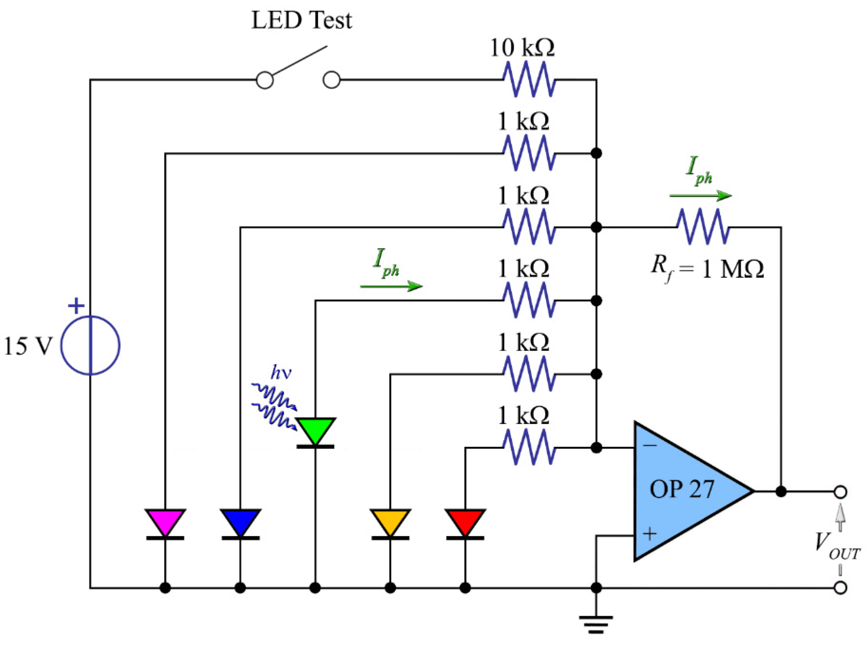
The section used to control the LED used as light receiver is achieved according circuit shown in the Figure 14.
In this circuit LEDs are used as light sensors (Rx section).
The Rx section, used to convert the incident light into an electrical signal, is made with five LEDs of different colors (the LEDs are used as wavelength-selective light sensors).
By means of the Tx section, light with different wavelength (using LEDs with different colors) can be produced. This light can hit the LEDs of the Rx section. If the wavelength of the incident light is greater than or equal to that which the LEDs used as light sensors could emit, in the latter a photo current is produced. Coupling LEDs by varying the color, it is possible to evaluate the generation of an electric current or not. To detect the emitted photocurrent of LEDs, a low noise OP 27 operational amplifier is used in configuration current to voltage converter, i.e., a transimpedance amplifier. In the proposed circuit, the output voltage of operational amplifier (VOUT) is directly proportional to the current given to the inverting terminal of the op amp (the photocurrent generated by enlightened LED).
Resistors have been inserted in series with the LEDs. From the point of view of the transimpedance amplifier they are inessential. On the other hand, they are fundamental for being able to “turn on” the LEDs to be able to control the light’s color emitted. Indeed, before beginning the educational experiments, the switch named LED Test can be used to check the color of the light emitted by the LEDs. All to check that what will then be studied is consistent with what was expected. In our system, a self-made structure is positioned above the Rx LEDs in order to facility the coupling between Rx and Tx LED.
Considering the properties of the operational amplifier, when an LED is hit by appropriate radiation, it generates photocurrent; the wavelength of the incident radiation must be less than the wavelength of the light that the LED can emit. Due to the properties of the operational amplifier, this photocurrent flows in the feedback resistance (in our circuit Rf = 1 MΩ). For this reason, the output voltage of the operational amplifier is:
In Equation (12), Iph represents the generated photocurrent, Rf is the feedback resistor and VOUT is the op amp output voltage. By means of circuit illustrated in Figure 14, we have a voltage output proportional to the light intensity of the Tx LED.
Our system allows two important checks to be carried out on the internal photoelectric effect.
- ▪
- Verify that the photoelectric effect occurs only if hν > Eg.
- ▪
- Prove that the energy carried by the light is quantized.
The tests were carried out by lighting a single receiving LED with a single transmitting LED. The two LEDs were positioned face-to-face by means of a self-made structure.
When a wavelength is detected, a photocurrent proportional to the incident power is generated; the photocurrent is proportional to the responsivity of the led. In particular, it is possible to verify that the photocurrent is generated only if the energy of the incident photons is greater than the bandgap energy of the semiconductor used to realize the receiving LED. In other words, if the wavelength of the LED illuminator is less than the wavelength that would “emit” LED receiver. For example, with our system it is possible to verify that if the yellow LED is illuminated with red light there is no generation of photocurrent, on the contrary it generates photocurrent if it irradiates with yellow, green, blue or UV radiation.
Another important test that can be carried out is to verify that we have , whatever the luminous intensity of the incident radiation. For example, if we use Red LED to light up a yellow LED, the photocurrent is not generated, any intensity of red light is used.
The system is able to check that the generated current is proportional to the number of incident photons. Using the multi-turn trimmer, we can vary the current flowing in the transmitter LED. The luminous intensity (the number of photons emitted) is proportional to the bias current.
If we couple the transmitter LED with the same type of LED used as a receiver, we can verify that the generated photocurrent is proportional to the incident luminous intensity.
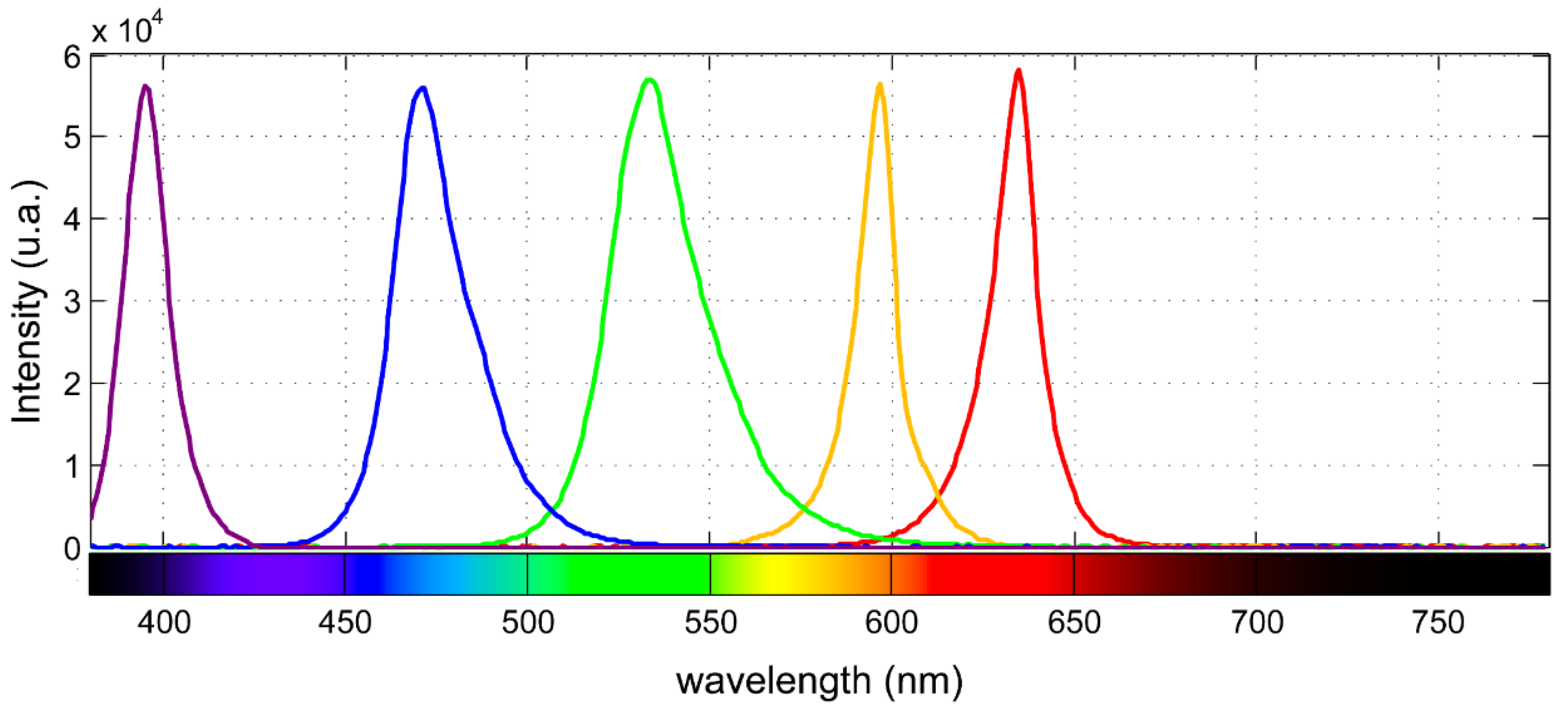
List of LED used as receivers and transmitters is shown in Table 1.
Figure 15 shows the emission spectra of the used LEDs.
5. LED-to-LED Communication
Current studies on the possibility of using Visible Light Communication (VLC) has received great attention from industry and the academic community [45,46,47,48,49]. VLC systems transmit information wirelessly by rapidly pulsing visible light using light emitting diodes (LEDs).
Some recent works showed the possibility to make a connection by the Light Fidelity (Li-Fi) technology. Li-Fi is a “post-Wi-Fi” wireless technology based on the use of Visible Light Communication (VLC) (instead of radio frequency waves for Wi-Fi). Li-Fi is a VLC system that uses light from Light-Emitting Diodes (LEDs) as a medium to deliver networked, mobile and high-speed communications. Li-Fi principle relies on the data transmission by amplitude modulation of light sources [50,51,52]. The Li-Fi technology can be used for various purposes, it matters the data transmission through LEDs thus all the screens which illuminate light can be served as a platform for data communication. The screen of the mobile phone, television, bulbs can act as a source of light. On the other hand, the receiving platform, the photo detector can be replaced by a camera in mobile phone for scanning and retrieving data. This technology has the advantage of being useful in electromagnetic sensitive areas such as in aircraft cabins, in hospitals, nuclear sites, without causing electromagnetic interference.
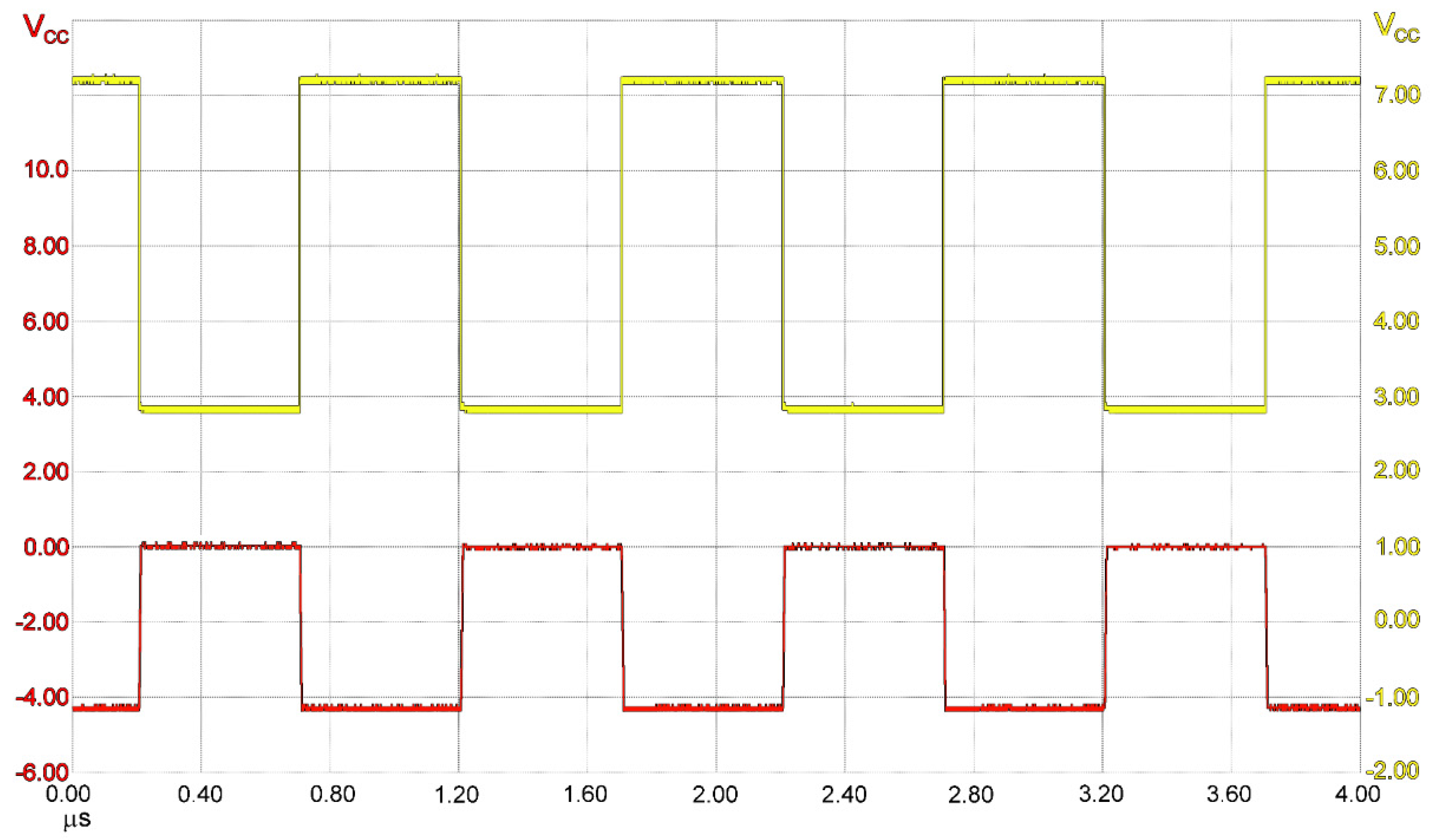
In proposed system, through an external function generator, it is possible to modulate the power supply of the LED (see the circuit shown in Figure 13). In order to demonstrate the ability to transmit/receive information via LEDs, the Tx LED current has been modulated with a square wave at 1 MHz. Such modulated light beam was received by the light receiving LED. The Figure 16 shows the waveforms of the source signal (Tx—red waveform) and the output voltage obtained from the LED Rx (blue waveform).
The LEDs have very low parasitic capacities. This property makes them suitable to realize optical communications with high bit rate. Data transmission at rates exceeding 100 Mbit/s is possible using LEDs as transmitter and receiver [53].
6. Conclusions
A low-cost device for experimental demonstration of photoelectric effect has been proposed. Tool based both on the light emission/detection capability of the LEDs. The simplicity and safety of the device allows it to be widely used for the didactic demonstration of the corpuscular nature of light. Furthermore, the tool allows to familiarize with the employment of LEDs as selective light detector. This property of LEDs is extremely interesting to realize the optical wireless communication (Li-Fi); an interesting alternative to the classic Radio Frequency wireless Communication (Wi-Fi).
Author Contributions
Conceptualization, G.S.S.; methodology, G.S.S.; validation, G.S.S. and F.L.; formal analysis, F.L.; investigation, G.S.S. and M.L.; resources, F.L.; data curation, M.L.; writing—original draft preparation, G.S.S. and M.L.; writing—review and editing, F.L. and G.S.S.; visualization, F.L.; supervision, F.L.; funding acquisition, F.L.
Funding
This research received no external funding and The APC was funded by Fabio Leccese.
Conflicts of Interest
The authors declare no conflict of interest.
References
- Müller, R.; Wiesner, H. Teaching quantum mechanics on an introductory level. Am. J. Phys. 2002, 70, 200–209. [Google Scholar] [Green Version]
- Planinši, G.; Etkina, E. Light-emitting diodes: A hidden treasure. Phys. Teach. 2014, 52, 94–99. [Google Scholar] [CrossRef]
- Schirripa Spagnolo, G.; Martocchia, A.; Papalillo, D.; Cozzella, L. Simple educational tool for digital speckle shearography. Eur. J. Phys. 2012, 33, 733–750. [Google Scholar] [CrossRef]
- Hadzidaki, P.; Kalkanis, G.; Stavrou, D. Quantum mechanics: A systemic component of the modern physics paradigm. Phys. Educ. 2000, 35, 386–392. [Google Scholar] [CrossRef]
- Feynman, R. QED: The Strange Theory of Light and Matter; Princeton University Press: Princeton, NJ, USA, 1985; p. 15. [Google Scholar]
- Klassen, S. The Photoelectric effect: Reconstructing the story for the physics classroom. Sci. Educ. 2011, 20, 719–731. [Google Scholar] [CrossRef]
- Hertz, H. Ueber strahlen electrischer kraft. Annalen der Physik 1889, 272, 769–783. [Google Scholar] [CrossRef]
- Lenard, P. Über die lichtelektrische Wirkung. Annalen der Physik 1902, 8, 149–198. [Google Scholar] [CrossRef]
- Einstein, A. Einstein’s proposal of the photon concept—A translation of the annalen der physik paper of 1905. Am. J. Phys. 1965, 33, 1–16. [Google Scholar]
- Boys, D.W.; Cox, M.E.; Mykolajenko, W. Photoelectric effect revisited (or an inexpensive device to determine h/e). Am. J. Phys. 1978, 46, 133. [Google Scholar] [CrossRef]
- Garver, W.P. The photoelectric effect using LEDs as light sources. Phys. Teach. 2006, 44, 272–275. [Google Scholar] [CrossRef]
- Loparco, F.; Malagoli, M.S.; Rainò, S.; Spinelli, P. Measurement of the ratio h/e with a photomultiplier tube and a set of LEDs. Eur. J. Phys. 2017, 38, 025208. [Google Scholar] [CrossRef]
- Pimputkar, S.; Speck, J.S.; DenBaars, S.P.; Nakamura, S. Prospects for LED lighting. Nat. Photonics 2009, 3, 180–182. [Google Scholar] [CrossRef]
- Khan, T.Q.; Bodrogi, P.; Vinh, Q.T.; Winkler, H. LED Lighting: Technology and Perception; John Wiley & Sons, Inc.: Hoboken, NJ, USA, 2015. [Google Scholar]
- Papalillo, D.; Del Vecchio, P.; Schirripa Spagnolo, G. LED applications in road and railway signals: Is it possible to fit specifications? In Proceedings of the Photonics Prague 2011, Prague, Czech Republic, 11 October 2011. [Google Scholar] [CrossRef]
- Schirripa Spagnolo, G.; Papalillo, D.; Martocchia, A.; Makary, G. Application of LEDs to traffic signal. In Proceedings of the 2012 11th International Conference on Environment and Electrical Engineering, Venice, Italy, 18–25 May 2012; pp. 864–868. [Google Scholar] [CrossRef]
- Schirripa Spagnolo, G.; Papalillo, D.; Martocchia, A. Light emitting diode in stationary transportation applications: Wavelength response to varying temperature. In Proceedings of the SPIE OPTO 2012, San Francisco, CA, USA, 2 February 2012. [Google Scholar]
- Schirripa Spagnolo, G.; Papalillo, D.; Malta, C.; Vinzani, S. LED railway signal vs full compliance with colorimetric specification. Int. J. Transp. Dev. Integr. 2017, 1, 568–577. [Google Scholar] [CrossRef]
- Heber, J. Nobel Prize 2014: Akasaki, Amano & Nakamura. Nat. Phys. 2014, 10, 791. [Google Scholar]
- Akasaki, I.; Amano, H.; Nakamura, S. Blue LEDs—Filling the World with New Light. R. Swed. Acad. Sci. Nobel Prize Phys. 2014. Available online: http://www.theo-physik.uni-kiel.de/~bonitz/D/vorles_14ws/popular-physicsprize2014.pdf (accessed on 12 October 2019).
- Mims, F.M. Sun photometer with light-emitting diodes as spectrally selective detectors. Appl. Opt. 1992, 31, 6965–6967. [Google Scholar] [CrossRef] [PubMed]
- RayChaudhuri, B.; Sen, C. Light emitting diode as sensor for miniature multispectral radiometer. Appl. Phys. B 2009, 95, 141–144. [Google Scholar] [CrossRef]
- Rajagopal, S.; Roberts, R.D.; Lim, S.K. IEEE 802.15.7 visible light communication: Modulation schemes and dimming support. IEEE Commun. Mag. 2012, 50, 72–82. [Google Scholar] [CrossRef]
- Medina, C.; Zambrano, M.; Navarro, K. LED based visible light communication: Technology, applications and challenges-a survey. Int. J. Adv. Eng. Technol. 2015, 8, 482–495. [Google Scholar]
- Incipini, L.; Belli, A.; Palma, L.; Ballicchia, M.; Piereoni, P. Sensing Light with LEDs: Performance Evaluation for IoT Applications. J. Imaging 2017, 3, 50. [Google Scholar] [CrossRef]
- Matheus, L.E.M.; Vieira, A.B.; Vieira, L.F.; Vieira, M.A.; Gnawali, O. Visible light communication: Concepts, applications and challenges. IEEE Commun. Surv. Tutor. 2019, 1, 1. [Google Scholar] [CrossRef]
- Whitefield, R.J.; Brady, J.J. New value for work function of sodium and the observation of surface- plasmon effects. Phys. Rev. Lett. 1971, 26, 380–383. [Google Scholar] [CrossRef]
- Lloyd, D.R. What was measured in Millikan’s study of the photoelectric effect? Am. J. Phys. 2015, 83, 765–772. [Google Scholar] [CrossRef]
- Sze, S.M.; Ming-Kwei Lee, M.K. Semiconductor Devices: Physics and Technology, 3rd ed.; John Wiley & Sons: Hoboken, NJ, USA, 2006. [Google Scholar]
- Diaz, L.; Smith, C.A. Investigating the photoelectric effect using LEDs and a modular spectroscope. J. Chem. Educ. 2005, 82, 906–908. [Google Scholar] [CrossRef]
- Miyazaki, E.; Itami, S.; Araki, T. Using a light-emitting diode as a high-speed, wavelength selective photodetector. Rev. Sci. Instrum. 1998, 69, 3751–3754. [Google Scholar] [CrossRef]
- Rossiter, J.; Mukai, T. A novel tactile sensor using a matrix of LEDs operating in both photoemitter and photodetector modes. In Proceedings of the SENSORS, 2005 IEEE, Irvine, CA, USA, 31 October–3 November 2005. [Google Scholar]
- O’Toole, M.; Diamond, D. Absorbance based light emitting diode optical sensors and sensing devices. Sensors 2008, 8, 2453–2479. [Google Scholar] [CrossRef]
- Jo, Y.C.; Kim, H.N.; Kang, J.H.; Hong, H.K.; Choi, Y.S.; Jung, S.W.; Kim, S.P. Novel wearable-type biometric devices based on skin tissue optics with multispectral LED–photodiode matrix. Jpn. J. Appl. Phys. 2017, 56. [Google Scholar] [CrossRef]
- Petit, M.; Michez, L.; Raimundo, J.M.; Dumas, P. Electrical and optical measurements of the bandgap energy of a light-emitting diode. Phys. Educ. 2016, 51, 025003. [Google Scholar] [CrossRef]
- Einstein, A. Relativity, 1st ed.; Routledge: London, UK, 2013. [Google Scholar]
- Bloch, F.Z. Über die quantenmechanik der elektronen in kristallgittern. Zeitschrift für Physik 1929, 52, 555–600. [Google Scholar] [CrossRef]
- Kronig, R.d.L.; Penney, W.G. Quantum mechanics of electrons in crystal lattices. Proc. R. Soc. Lond. A 1931, 130, 499–513. [Google Scholar] [CrossRef]
- Herman, F. Theoretical investigation of the electronic energy band structure of solids. Rev. Mod. Phys. 1958, 30, 102–122. [Google Scholar] [CrossRef]
- Shockley, W.; Last, J.T. Statistics of the charge distribution for a localized flaw in a semiconductor. Phys. Rev. 1957, 107, 392–396. [Google Scholar] [CrossRef]
- Wagner, E.P. Investigating bandgap energies, materials, and design of light-emitting diodes. J. Chem. Educ. 2016, 93, 1289–1298. [Google Scholar] [CrossRef]
- Lorenz, M.R. Visible light from semiconductors: Luminescence from p-n junctions and potential uses of solid state light sources are discussed. Science 1968, 159, 1419–1423. [Google Scholar] [CrossRef] [PubMed]
- Feng, Z.C. Handbook of Solid-State Lighting and LEDs; CRC Press: Boca Raton, FL, USA, 2017. [Google Scholar]
- Horowitz, P.; Winfield Hill, W. The Art of Electronics, 3rd ed.; Cambridge University Press: Cambridge, UK, 2015. [Google Scholar]
- Komine, T.; Nakagawa, M. Fundamental analysis for visible-light communication system using LED lights. IEEE Trans. Consum. Electron. 2004, 50, 100–107. [Google Scholar] [CrossRef]
- Suzuki, K.; Asahi, K.; Watanabe, A. Basic study on receiving light signal by LED for bidirectional visible light communications. Electron. Commun. Jpn. 2015, 98, 1–9. [Google Scholar] [CrossRef]
- Zuo, Y.; Zhang, J.; Qu, J. Power allocation optimization design for the quadrichromatic LED based VLC systems with illumination control. Crystals 2019, 9, 169. [Google Scholar] [CrossRef]
- Monteiro, E.; Hranilovic, S. Constellation design for color-shift keying using interior point methods. In Proceedings of the 2012 IEEE Globecom Workshops, Anaheim, CA, USA, 3–7 December 2012; pp. 1224–1228. [Google Scholar]
- Leccese, F.; Cagnetti, M.; Ferrone, A.; Pecora, A.; Maiolo, L. An infrared sensor Tx/Rx electronic card for aerospace applications. In Proceedings of the 2014 IEEE Metrology for Aerospace (MetroAeroSpace), Benevento, Italy, 29–30 May 2014; pp. 353–357. [Google Scholar]
- Verma, S.K.; Madan, K.; Kaur, G. Future of visible light communication with li-fi technology: A review. Int. J. Innov. Res. Technol. 2015, 2, 82–85. [Google Scholar]
- Dimitrov, S.; Haas, H. Principles of LED Light Communications: Towards Networked Li-Fi; Cambridge University Press: Cambridge, UK, 2015. [Google Scholar]
- Masson, É.; Berbineau, M. Railway applications requiring broadband wireless communications. In Broadband Wireless Communications for Railway Applications; Springer: Cham, Switzerland, 2017. [Google Scholar]
- Stepniak, G.; Kowalczyk, M.; Maksymiuk, L.; Siuzdak, J. Transmission beyond 100 Mbit/s using LED both as a transmitter and receiver. IEEE Photonics Technol. Lett. 2015, 27, 2067–2070. [Google Scholar] [CrossRef]
Figure 1.
Electrons in a metal can be modelled as particles in a potential well. Highest lying electrons at Energy Φ (Fermi level) known as “work function”.
Figure 1.
Electrons in a metal can be modelled as particles in a potential well. Highest lying electrons at Energy Φ (Fermi level) known as “work function”.

Figure 2.
The Photoelectric Effect involves the irradiating a metal surface with photons of sufficiently high energy to causes electrons to be ejected from the metal. Sodium work function 2.75 eV [27,28]. (a) shows a sketch of a photoelectric test device. (b) shows the typical imagine used to explain the photoelectric effect.

Figure 3.
Electronic band structure of solids.

Figure 4.
Difference between the external and the internal photoelectric effect.

Figure 5.
Energy bands of electrons in a metal, semiconductor and insulator. Starting from the Fermi function [41], the probability of occupation of energy levels in valence band and conduction band is the Fermi level. In pure semiconductor (named intrinsic), the number of holes in valence band is equal to the number of electrons in the conduction band. Hence, the probability of occupation of energy levels in conduction band and valence band are equal. Therefore, the Fermi level for the intrinsic semiconductor lies in the middle of forbidden band.

Figure 6.
Simplified band diagram of a semiconductor. When a radiative transition occurs emitting a photon with an energy Eg ≈ h⋅ν. (a) electron-hole pair production. (b) electron-hole pair recombination with photon emission.
Figure 6.
Simplified band diagram of a semiconductor. When a radiative transition occurs emitting a photon with an energy Eg ≈ h⋅ν. (a) electron-hole pair production. (b) electron-hole pair recombination with photon emission.

Figure 7.
(a) n-type semiconductors have dopant atoms with one “extra” electron mixed into the material. This forms a dopant band just below the conduction band allowing ionization of electrons to the conduction band with room temperature thermal energy. The extra electrons that are charge carriers in the circuit are represented by dots. The holes are also charge carriers in the circuit and are represented by circles. (b) p-type semiconductors have dopant atoms with one “less” electron mixed into the material. This forms an empty dopant band just above the valence band.

Figure 8.
(a) n-type semiconductors have dopant atoms with one “extra” electron mixed into the material. This forms a dopant band just below the conduction band allowing ionization of electrons to the conduction band with room temperature thermal energy. The extra electrons that are charge carriers in the circuit are represented by dots. (b) At equilibrium the two current (drift and diffusion) have the same magnitude, but flow in opposite directions.

Figure 9.
LED p-n junction at forward bias.

Figure 10.
LED p-n junction used as light sensor. (a) creation of electron-hole pairs (b) phenomenon of the photo-current (c) sketch of a LED in which a photo-current flows.
Figure 10.
LED p-n junction used as light sensor. (a) creation of electron-hole pairs (b) phenomenon of the photo-current (c) sketch of a LED in which a photo-current flows.

Figure 11.
Schematic representation of realized system demonstration of the photoelectric effect. The system is realized with two distinct functional sections: (a) piloting of the LED used as a light transmitter; (b) LEDs used as light receivers.
Figure 11.
Schematic representation of realized system demonstration of the photoelectric effect. The system is realized with two distinct functional sections: (a) piloting of the LED used as a light transmitter; (b) LEDs used as light receivers.

Figure 12.
(a) The apparatus used for demonstration of the photoelectric effect. (b) Section used to control the LED used as light source. (c) Section used to control the LEDs used as receivers.
Figure 12.
(a) The apparatus used for demonstration of the photoelectric effect. (b) Section used to control the LED used as light source. (c) Section used to control the LEDs used as receivers.

Figure 13.
Circuit used for driving the LEDs used as light source (Tx section).

Figure 14.
Circuit used to convert light into output voltage.

Figure 15.
Emission spectra of the used LEDs.

Figure 16.
In yellow, waveform used to modulate the light intensity of the LED used as Tx. In red, waveform of the signal detected by the LED used as Rx. Yellow LED was employed as light source and red LED was used as receiver.
Figure 16.
In yellow, waveform used to modulate the light intensity of the LED used as Tx. In red, waveform of the signal detected by the LED used as Rx. Yellow LED was employed as light source and red LED was used as receiver.


Table 1.
List of LEDs used in the systems.
| Color | Model | Dominant Wavelength (nm) | Technology |
|---|---|---|---|
| Red | Kingbright_ L-7113SEC-E | 630 nm | AlGaInP |
| Yellow | Kingbright_L-53SYC | 595 nm | AlGaInP |
| Green | Nichia NSPG520AS | 520 nm | InGaN |
| Blue | Kingbright_L-7113QBC-D | 465 nm | InGaN |
| Violet | BIVAR UV5TZ-390-30 | 390 nm | InGaN |
© 2019 by the authors. Licensee MDPI, Basel, Switzerland. This article is an open access article distributed under the terms and conditions of the Creative Commons Attribution (CC BY) license (http://creativecommons.org/licenses/by/4.0/).
Share and Cite
MDPI and ACS Style
Schirripa Spagnolo, G.; Leccese, F.; Leccisi, M. LED as Transmitter and Receiver of Light: A Simple Tool to Demonstration Photoelectric Effect. Crystals 2019, 9, 531. https://0-doi-org.brum.beds.ac.uk/10.3390/cryst9100531
AMA Style
Schirripa Spagnolo G, Leccese F, Leccisi M. LED as Transmitter and Receiver of Light: A Simple Tool to Demonstration Photoelectric Effect. Crystals. 2019; 9(10):531. https://0-doi-org.brum.beds.ac.uk/10.3390/cryst9100531
Chicago/Turabian StyleSchirripa Spagnolo, Giuseppe, Fabio Leccese, and Mariagrazia Leccisi. 2019. "LED as Transmitter and Receiver of Light: A Simple Tool to Demonstration Photoelectric Effect" Crystals 9, no. 10: 531. https://0-doi-org.brum.beds.ac.uk/10.3390/cryst9100531
Note that from the first issue of 2016, this journal uses article numbers instead of page numbers. See further details here.