Ambipolar Transport in Methylammonium Lead Iodide Thin Film Transistors


Department of Information Display, Kyung Hee University, Seoul 130-701, Korea
*
Author to whom correspondence should be addressed.
Crystals 2019, 9(10), 539; https://0-doi-org.brum.beds.ac.uk/10.3390/cryst9100539
Submission received: 15 September 2019
/
Revised: 17 October 2019
/
Accepted: 17 October 2019
/
Published: 19 October 2019
(This article belongs to the Special Issue Advances in Thin Film Materials and Devices)
Abstract
:We report clear room temperature ambipolar transport in ambient-air processed methylammonium lead iodide (MAPbI3) thin-film transistors (TFTs) with aluminum oxide gate-insulators and indium-zinc-oxide source/drain electrodes. The high ionicity of the MAPbI3 leads to p-type and n-type self-doping, and depending on the applied bias we show that simultaneous or selective transport of electrons and/or holes is possible in a single MAPbI3 TFT. The electron transport (n-type), however, is slightly more pronounced than the hole transport (p-type), and the respective channel resistances range from 5–11 and 44–55 MΩ/μm. Both p-type and n-type TFTs show good on-state characteristics for low driving voltages. It is also shown here that the on-state current of the n-type and p-type TFTs is highest in the slightly PbI2-rich and MAI-rich films, respectively, suggesting controllable n-type or p-type transport by varying precursor ratio.
1. Introduction
Hybrid organic-inorganic perovskites are emerging materials with remarkable optoelectronic properties [1]. Among them, methylammonium lead iodide (CH3NH3PbI3) has proven to be an exceptional light harvester for solar cells, recording power conversion efficiencies of over 20% in just a few years [2,3,4,5,6]. Despite low-temperature (<150 °C) processing, the density of electronic defect states in CH3NH3PbI3 (MAPbI3) is surprisingly low [7,8,9,10,11,12,13]. This combined with other unique properties such as high photoluminescence quantum yield, tunable bandgap, and a high absorption coefficient, are the reasons for the success of the MAPbI3 in photovoltaics (PV) [1,14]. In addition to PV applications, MAPbI3 is also appealing for several other applications, including light emitting diodes (LEDs) [8,10,11,15], thin-film transistors (TFTs) [16,17,18,19,20,21] and light emitting transistors (LETs) [2].
For large-area TFT applications, MAPbI3 enables low manufacturing costs, as it can be synthesized from simple precursors through solution processing or vapor deposition methods [17,18,19,20,21,22]. Additionally, MAPbI3 possesses high carrier mobility and a bandgap in the near-infrared energies, which can be easily tuned with chemical composition [23,24,25,26,27]. The ability to be fabricated from solution and its potential for high field-effect mobility (µFE) has been particularly interesting in flexible, printable or wearable devices, where the development of such a semiconductor is key [4].
Due to the existence of both the inorganic and organic components, MAPbI3 has the potential for ambipolar transport, where simultaneous or selective transport of electrons and/or holes is possible. Theoretical calculations have revealed that charged MA, Pb, and I vacancies have low formation energies [28,29], suggesting that the high ionicity of this material may lead to n-type or p-type self-doping. Furthermore, previous studies have shown that carrier concentration can vary over orders of magnitude, depending on the precursor ratio (MAI/PbI2) and thermal annealing conditions, thus resulting in preferential n-type or p-type transport characteristics [30]. Ambipolar transport enables the design of circuits with low-power dissipation and good noise margins, similar to those encountered in complementary metal–oxide semiconductor (CMOS) logic circuits. However, nearly all MAPbI3 TFTs in previous studies have been shown to transport only electrons (n-type) [17,18,31,32] with the exception of those measured at and below 198 K with high driving voltages (over 100 V) and/or doped with cesium (Cs) and formamidinium (FA) [2,33].
Here we investigate the room temperature (RT) ambipolar transport in the MAPbI3 TFTs by correlating charge carrier transport with the TFTs’ current–voltage (I–V) characteristics. In contrast to previous reports, we process the MAPbI3 in ambient air for room temperature stability and use a thin (32 nm) UV ozone-treated aluminum oxide (AlOx) gate-insulator (GI) to decrease the driving voltages.
2. Materials and Methods
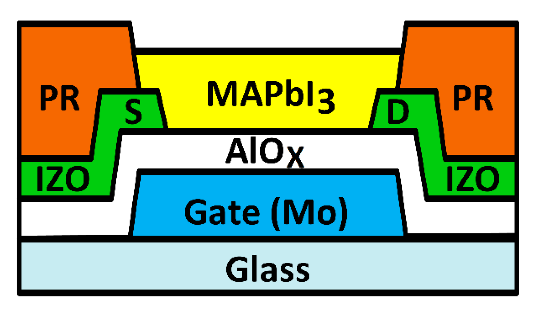
We fabricated the MAPbI3 TFTs on glass with the inverted coplanar structure (Figure 1). The gate electrode is a 40-nm-thick Mo layer deposited by sputtering at 280 °C. For the gate insulator (G. I), we used a 40-nm-thick AlOx layer spin coated from solution in ambient air (relative humidity = 50 ± 5, Temperature = 25 °C ± 2 °C). We prepared the AlOx solution by mixing aluminium chloride (AlCl3) (Merck Korea Ltd./Sigma-Aldrich Korea Ltd. ), acetonitrile (35%) (Merck Korea Ltd./Sigma-Aldrich Korea Ltd.), and ethyleneglycol (65%) (0.2 M) (Merck Korea Ltd./Sigma-AldrichKorea Ltd.). The solution is spin coated at 2000 rotations per min (rpm) for 30 s. Two layers were used to achieve the thickness of 40 nm and curing at 250 °C for five minutes was performed to evaporate the solvent, followed by 5 min UV ozone treatment. For film densification, we performed a final anneal for 2 h at 350 °C. Using Mo/AlOx/indium zinc oxide (IZO) structures (400 µm × 400 µm), the capacitance of the AlOx layer per unit area (COX) is estimated to be approximately 200 nF/cm2. We define the source and drain electrodes by patterning a 60 nm thick IZO layer deposited at 280 °C by sputtering. We spin-coated a positive photoresist (PR) (Sigma-Aldrich, Inc., Steinheim, Germany) layer on top of the source and drain electrodes and patterned it to form “banks” into which we spin coated the MAPbI3. The banks were necessary to avoid the use of photolithography processes directly on the hybrid perovskite because the MAPbI3 is vulnerable to wet processes.
After the formation of the banks, we subjected the samples to UV-ozone treatment (AHTECH LTS., Gyeonggi-do, South Korea) for 15 min before depositing the MAPbI3 in ambient air (at 25 °C and relative humidity of ~52%). The UV-ozone treatment modifies the surface of the AlOx G.I. for better MAPbI3 adhesion. To make the MAPbI3 solution, we dissolved precursors CH3NH3I (99.999%) (Greatcell Solar, Queanbeyan, Australia) and PbI2 (99.999%, Sigma-Aldrich) (1:1 molar ratio) (manufacturer, city, Country) in N, N dimethylformamide anhydrous, DMF (99.8%) (Merck Korea Ltd./Sigma-Aldrich Korea Ltd.), and added 50 μL of hydriodic acid (57 wt%) (Merck Korea Ltd./Sigma-Aldrich Korea Ltd.). We used MAI:PbI2 ratios of 0.5:1, 0.8:1, 1:1, and 1.2:1 and stirred the solutions for six hours at 60°C before spin-coating in ambient air. The spin-coating speed and time were respectively 6000 rpm and 70 s, achieving a thickness of ~130 nm for the MAPbI3. During the spin-coating process, we added 150 μL of toluene (99.8%, Sigma-Aldrich) (Merck Korea Ltd./Sigma-Aldrich Korea Ltd.) as an anti-solvent. The toluene reduces the crystallization time by rapidly reducing the solubility of the MAPbI3, thereby promoting fast nucleation and growth of crystals in the film.
As the MAPbI3 solutions sunk into the holes in the PR layer (Figure 1), it was not necessary to pattern the MAPbI3 films through photolithography. Note that direct photolithography on these hybrid materials may lead to contamination. Finally, we annealed the samples at 115 °C for 10 min on a hotplate to finish the crystallization process. We analyzed the physical properties of the films using X-ray photoelectron spectroscopy (XPS) (ULVAC-PHI, INCORPORATED, PHI 5000 VersaProbe, Kanagawa, Japan), atomic force microscope (AFM) images (Park Systems, XE-100, Suwon, Korea), X-ray diffraction (XRD) (Malvern Panalytical Ltd, X’Pert PRO, Royston, UK) and scanning electron microscope (SEM) images (Hitachi High Technologies, S-4700, Tokyo, Japan ). We respectively derived the μFE and threshold voltage (VTH) values from the slopes and intercepts of the linear regression lines of the ID1/2(VGS) plots in the saturation region (VDS > VGS – VTH), according to the equation, ID = (W/L)*COX*μFE*(VGS – VTH)2. Here, W, L, VGS, VDS, and ID denote the channel width, channel length, gate voltage, drain voltage, and drain current, respectively. We derived the μFE and VTH from the |IDS|1/2(VGS) plots. We estimated the subthreshold VGS swing (SS) by (d log (ID)/d VGS)−1.
3. Results
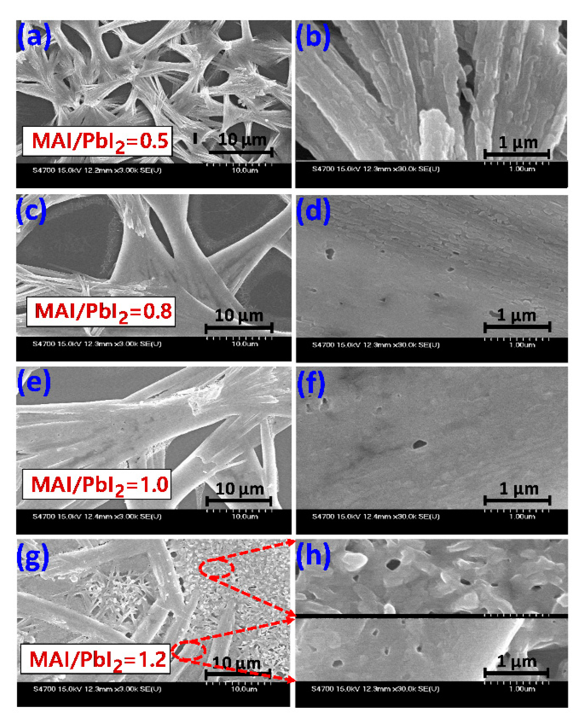
Consistent with previous reports [34], the ambient air-processed MAPbI3 films consisted of a network of thick dendritic bundles and the thickness of the bundles increased with increasing MAI/PbI2 ratio (Figure 2). This dendritic structure is common to films exposed to humidity during processing and it indicates anisotropic growth, where faster growth occurs along energetically favorable crystallographic directions [34]. Despite the poor film coverage, dendritic bundles are known for their good film conductivity and are thus desirable for lateral conduction in solution processed semiconductors [34]. Each of the bundles exhibited good crystallinity as seen from the high resolution SEM images (Figure 2b,d,f,h) and XRD analysis.
XRD measurements verified that the films were MAPbI3 films of the intended MAI/PbI2 ratios. The XRD patterns of all the four ambient air-processed MAPbI3 films contained sharp peaks at 2θ values of 13.9°, 28.2°, and 31.7°, the intensity of which increased with increasing MAI/PbI2 ratio (Figure 3). These peaks are respectively assigned to the (110), (220) and the (310) crystal planes of the MAPbI3 and they indicate high crystallinity in tetragonal phase [35]. Consistently, the intensity of the peak at the 2θ value of 12.67° gradually decreases with increasing MAI/PbI2 ratio until it completely disappears when the ratio exceeds one. This is the PbI2 peak and its absence indicates the absence of PbI2 residues in the film [36,37,38,39,40].
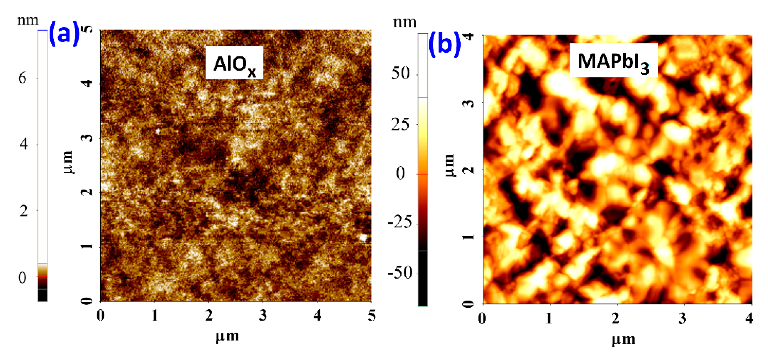
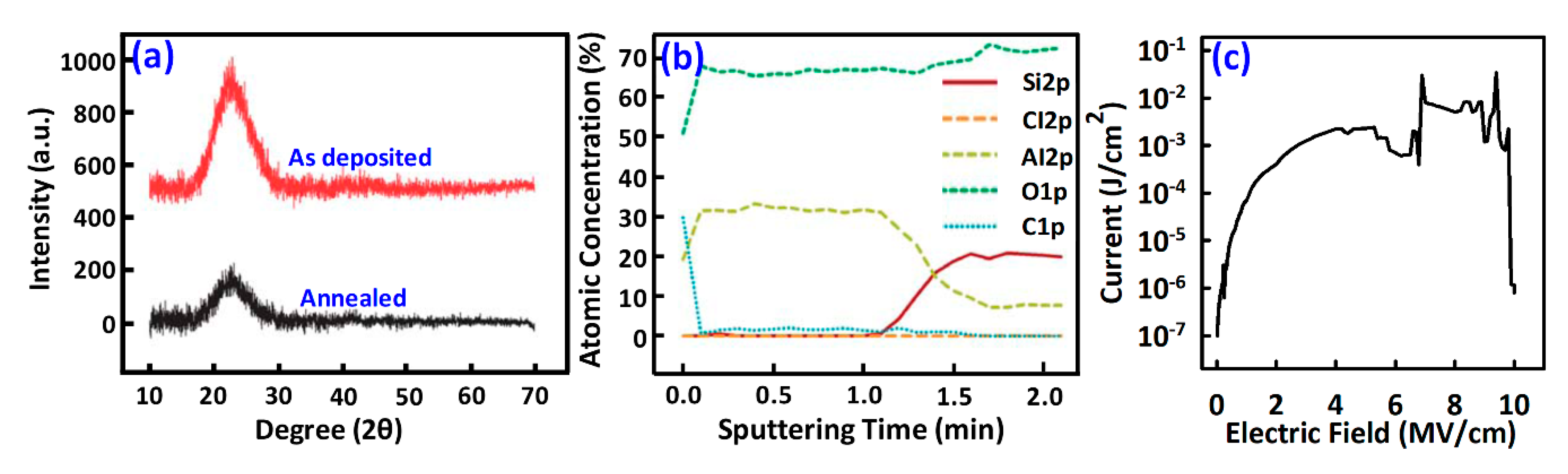
The AFM images of the AlOx and MAPbI3 film (MAI/PbI2 = 1.0) are shown in Figure 4a,b, respectively. The AlOx form a very smooth film with roughness of root mean square (rms) value approximately equal to 0.2 nm. However, the dendrites of the MAPbI3 film results in a much higher rms value of the roughness, reaching 40 nm. The AlOx is amorphous (Figure 5a) and its atomic concentrations are shown in Figure 5b. Using a TFT structure (Figure 1), we measured the breakdown voltage of the AlOx gate insulator to be 4 MV/cm Figure 5c). These results are consistent with previous reports [41].
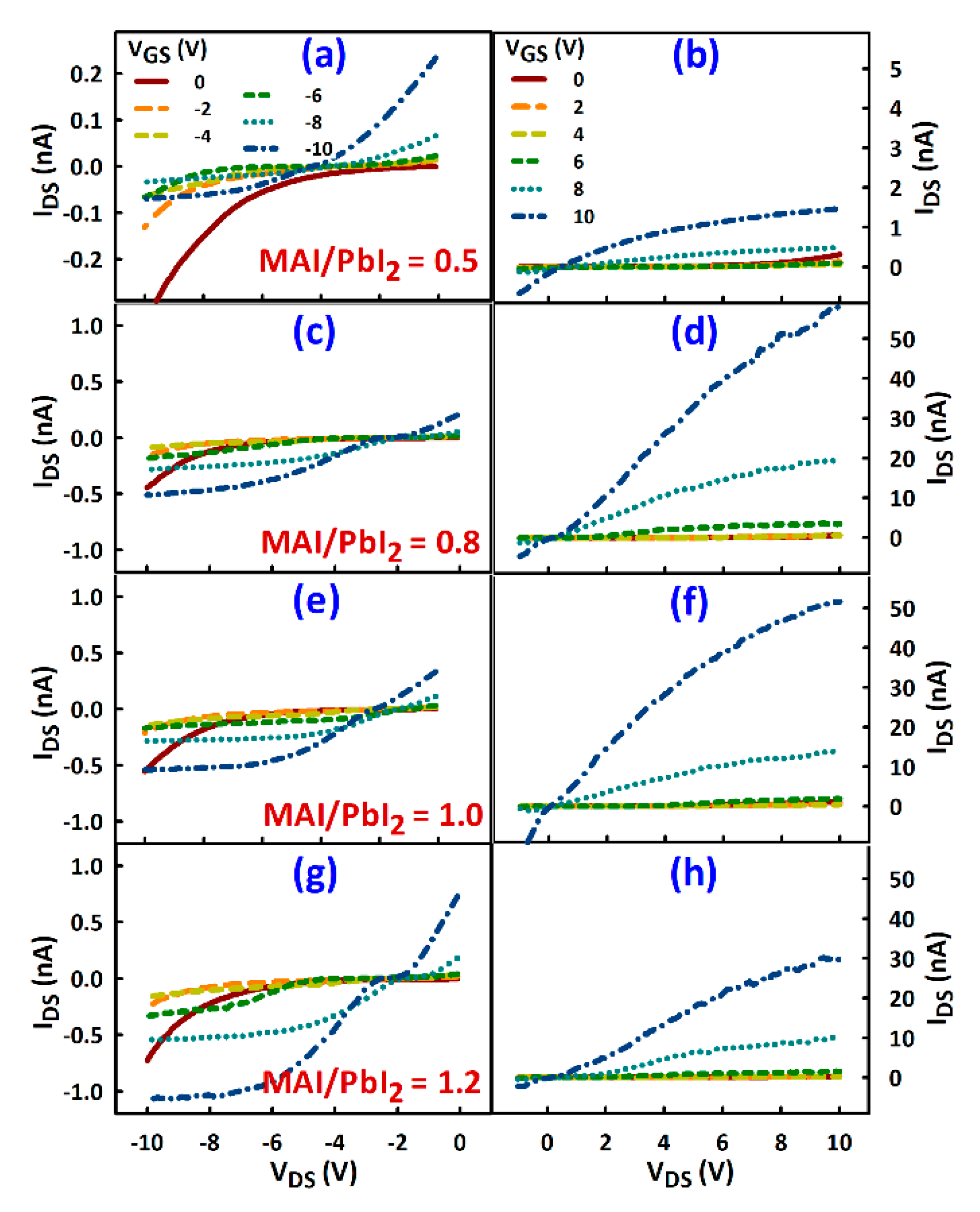
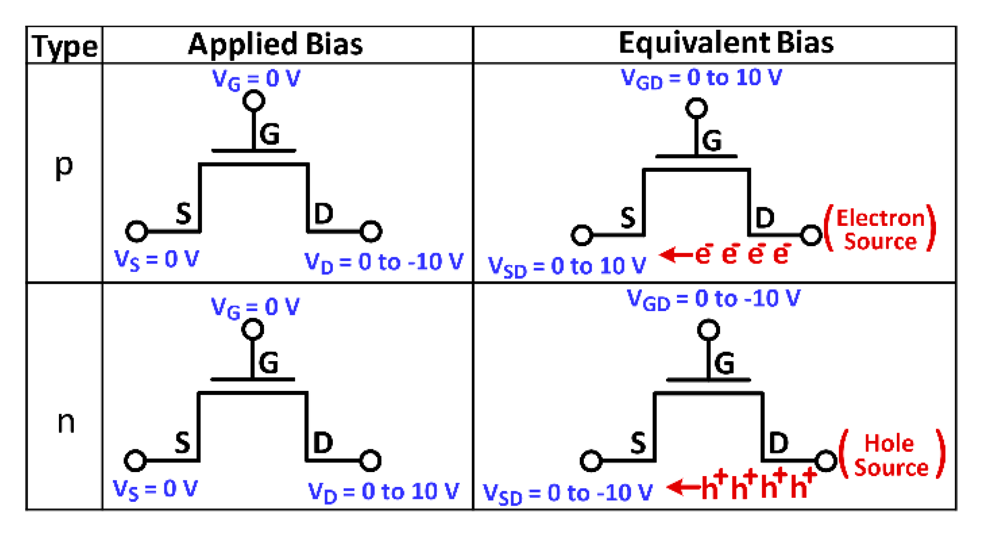
We observed clear room temperature ambipolar transport in the MAPbI3 TFTs. In unipolar enhancement mode TFTs, negligible ID flows across the channel when the VGS is equal to zero volts, unless the VGS is increased to a value greater than the VTH. For the MAPbI3 TFTs investigated herein, however, the ID increases rapidly with increasing |VDS| when VGS = 0 V (Figure 6). Under p-type bias conditions [Figure 6a], for instance, electrons are injected from the drain to the source for VDS < (VGS–VTHn). Here VTHn is the VTH for the n-type characteristics. The flow of current at VGS = 0 V is due to the presence of both hole and electron transport, and the choice of the carrier is determined by the equivalent bias conditions as shown in Figure 7.
When the VDS is swept from 0 to −10 V with the VGS fixed at zero volts, the equivalent bias conditions favor electron injection from the drain (see p-type characteristics in Figure 7). If the semiconductor supports bipolar transport, electron transport will dominate conduction under these bias conditions. This is the case for the MAPbI3 studied herein. The electron current under the p-type bias conditions (when VDS < (VGS – VTHn)) is similar to that of a TFT in the diode configuration (i.e., VGS = VDS. Although in saturation (VDS > VGS – VTH), the ID does not level-off but continues to exponentially increase with VDS in a manner similar to the current of a forward biased diode). As the VGS decreases from 0 to -6 V, the electron injection from the drain is shifted to smaller and smaller values of VDS because negative VGS depletes electrons. With further decrease in VGS (−8 to −10 V), holes accumulate in the channel and the injection of holes from the source to the drain is initiated. Under the hole transport, the output curves saturate at VDS = (VGS – VTHp), where VTHp is the VTH for the p-type characteristics (Figure 6a). Note that the direction of the current is the same for both the electron and hole transport (i.e., from the source to the drain). The significance of this is that the simultaneous or selective transport of electrons and/or holes is possible, depending on the bias conditions. Similarly, injection of holes from the drain is obtained under the n-type bias conditions when VGS = 0 V and VDS > (VGS – VTHp). The hole current under the n-type bias conditions is also similar to that of a TFT in the diode configuration (Figure 6b). With increasing VGS, hole injection from the drain shifts towards larger and larger values of VDS until electrons are the dominant carriers, and the output curves saturate at VDS = (VGS – VTHn).
It is interesting to see here that the ambipolar transport is apparent in all MAI/PbI2 ratios investigated (Figure 6a–h). However, the precursor composition has a clear effect on the magnitudes of each carrier transport. Hole and electron current increase with increasing MAI/PbI2 ratio, which is an indication of increased structural order in the MAPbI3 film with the increasing ratio. However, the electron transport appears to reach a peak when the MAI/PbI2 ratio 0.8, and decreases thereafter.
4. Discussion
A distinct characteristic of the MAPbI3 TFTs studied herein is the low driving voltages and stable room temperature operation. While the former is due to the thin high-k AlOx gate insulator, the latter is related to the ambient air processing. Ambient oxygen has been reported to have a passivation effect on the defects in perovskite materials [34,42,43]. It is also important to note that the ambipolar transport in the MAPbI3 is unbalanced. For MAI/PbI2 = 0.5, the electron current is about twenty times larger than the hole current (Figure 6a,b). Although the current of both carriers increases with increasing ratio, the electron current (Ie) increases much faster compared to the hole current (Ih), such that the Ie becomes about one hundred times larger than the Ih when the ratio reaches 0.8 (Figure 6e,f). However, the electron current appears to saturate, while the hole current continues to increase, when the ratio exceeds 0.8, such that the electron current becomes only fifty times larger than the hole current when the ratio reached 1.2.
We have recently shown that that small amounts of residual PbI2 (as in the case of MAI/PbI2 = 0.8) may boost electron transport and minimize ion migration by passivating ion vacancy defects in grain boundaries [44]. These ion vacancy defects are pathways for ion migration and their passivation improves lateral conduction and minimizes the vacancy-mediated migration of ions in the MAPbI3 film. This could be the reason for the high Ie exhibited by the TFTs with MAI/PbI2 = 0.8.
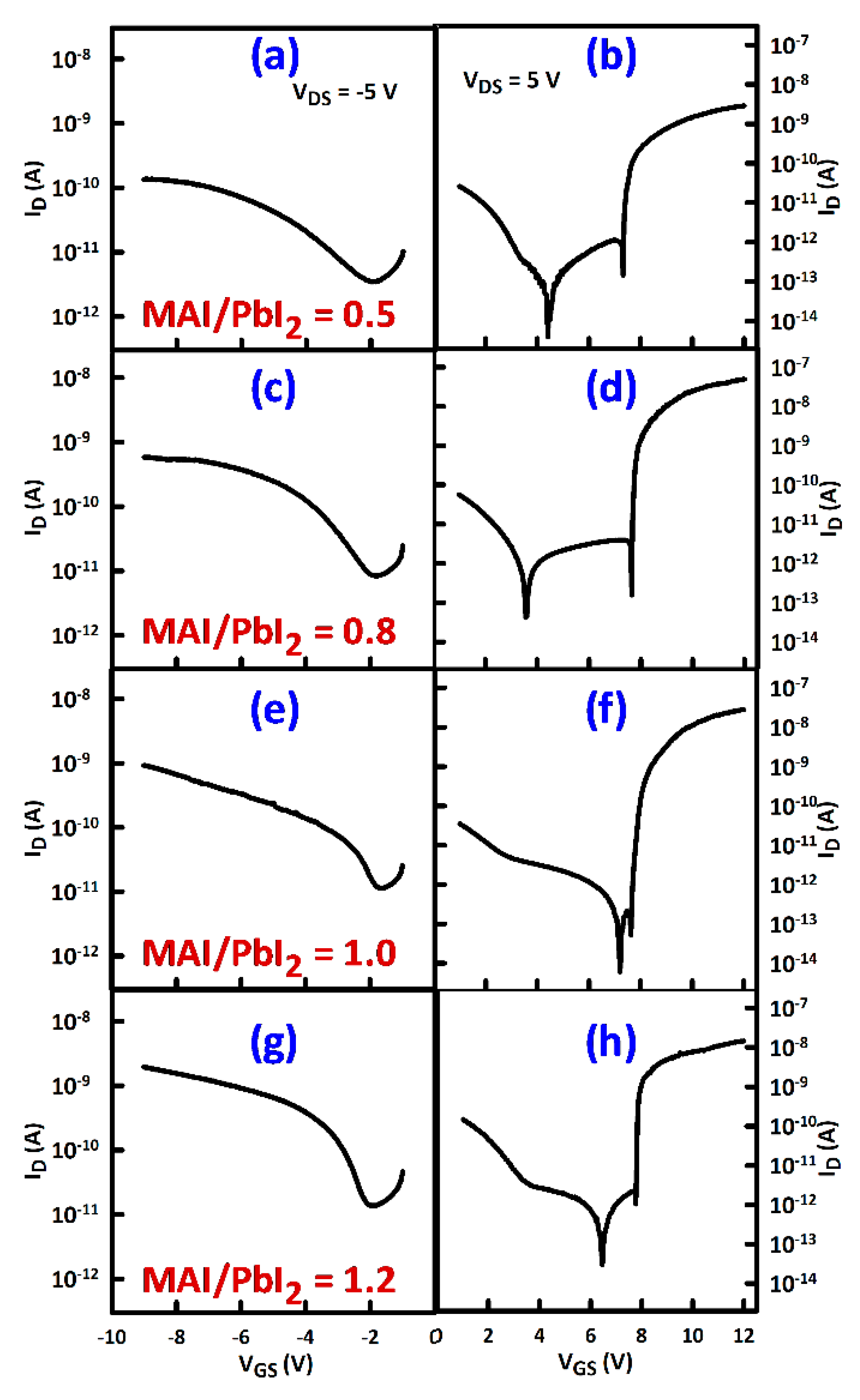
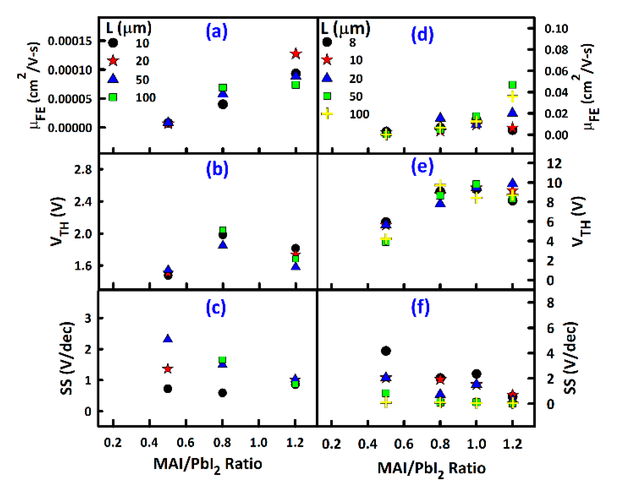
The ambipolar nature of the MAPbI3 also shows in the TFT transfer characteristics (Figure 8). The transfer characteristics are semi-log plots of the |ID| as a function of the VGS and they describe ON and OFF (switching) characteristics of the TFTs. In unipolar p-type TFTs, for example, negative VGS pushes the fermi level (EF) towards the valence band (EV). The μFE, VTH and SS values extracted from the saturation characteristics are shown in Figure 9. In the ON state, the ID due to the flow of electrons is over an order of magnitude larger than that due to the flow of holes, for all ratios (Figure 8). Furthermore, the ON/OFF ratio of the p-type transfer characteristics is about two orders of magnitude, whereas that of the n-type transfer characteristics is about five orders of magnitude. Consistently; the electron μFE is two orders of magnitude larger than that of the holes (Figure 9a,b).
Under the n-type bias conditions, the ID is due to holes flowing from the drain to the source, when the VGS is close to zero volts. Increasing the VGS positively results in the depletion of the holes and hence the decrease in ID. However, this off-state current is a sum of channel, gate leakage (IG) and displacement currents. As a result, negative current can be recorded at the drain when the IG dominates the three, which is the reason for the small hump in the n-type semi-log plots of |ID| (see Figure 8b,d,f,h). This hump comes from |IG| before the TFT turns ON. When the VGS is greater than seven volts, the accumulation of electrons is initiated and the ID is due to electrons flowing from the source to the drain. The concentration of these electrons increases with VGS and the opposite is true for the hole current.
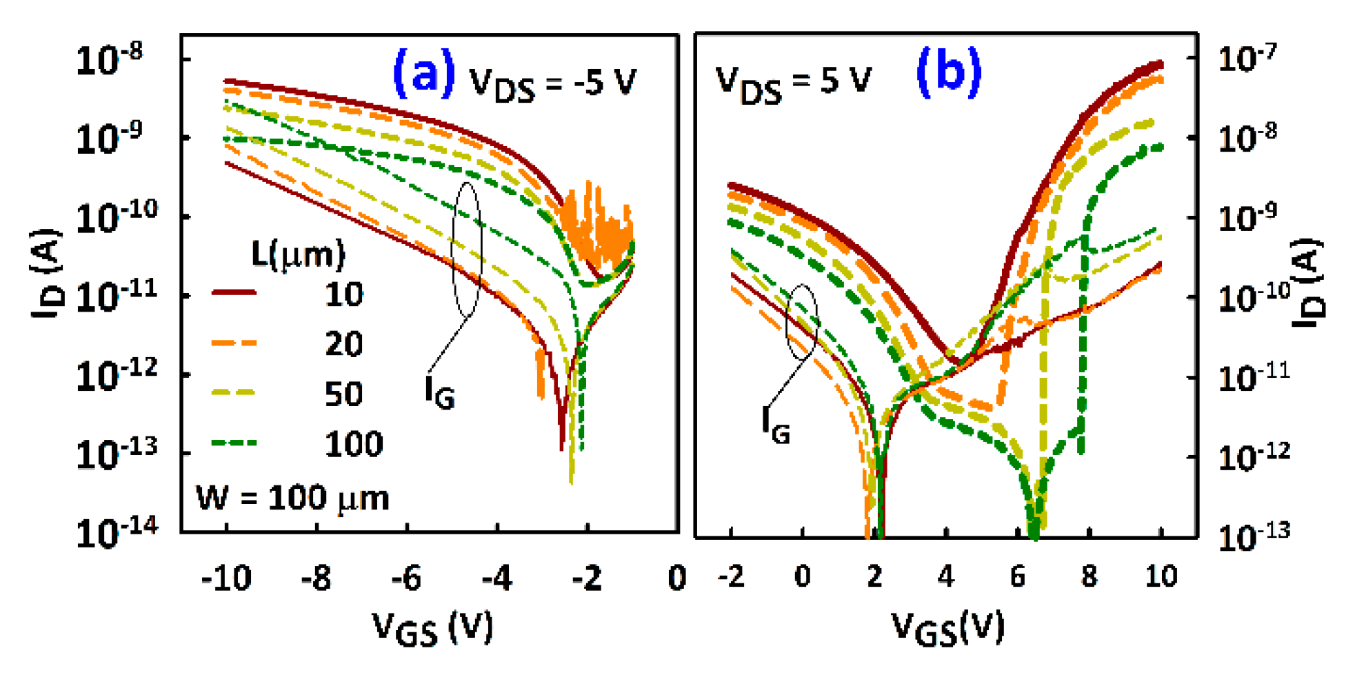
The IG of the TFTs presented herein is quite significant, given the relatively low ON state currents of the TFTs. Figure 10 shows the transfer characteristics of TFTs with varying channel length (L) and the IG curves for the MAI/PbI2 ratio of 1.2. The MAI/PbI2 ratio of 1.2 is shown here because it achieves the highest Ih. The ID scaled proportionally with L for both the hole (Figure 10a) and electron (Figure 10b) transport. For both p-type and n-type characteristics, the IG ranges from 0.1 to 1 nA in the ON state. The relatively high IG is due to the thin (40 nm) gate insulator and can be decreased by increasing the thickness of the gate insulator.
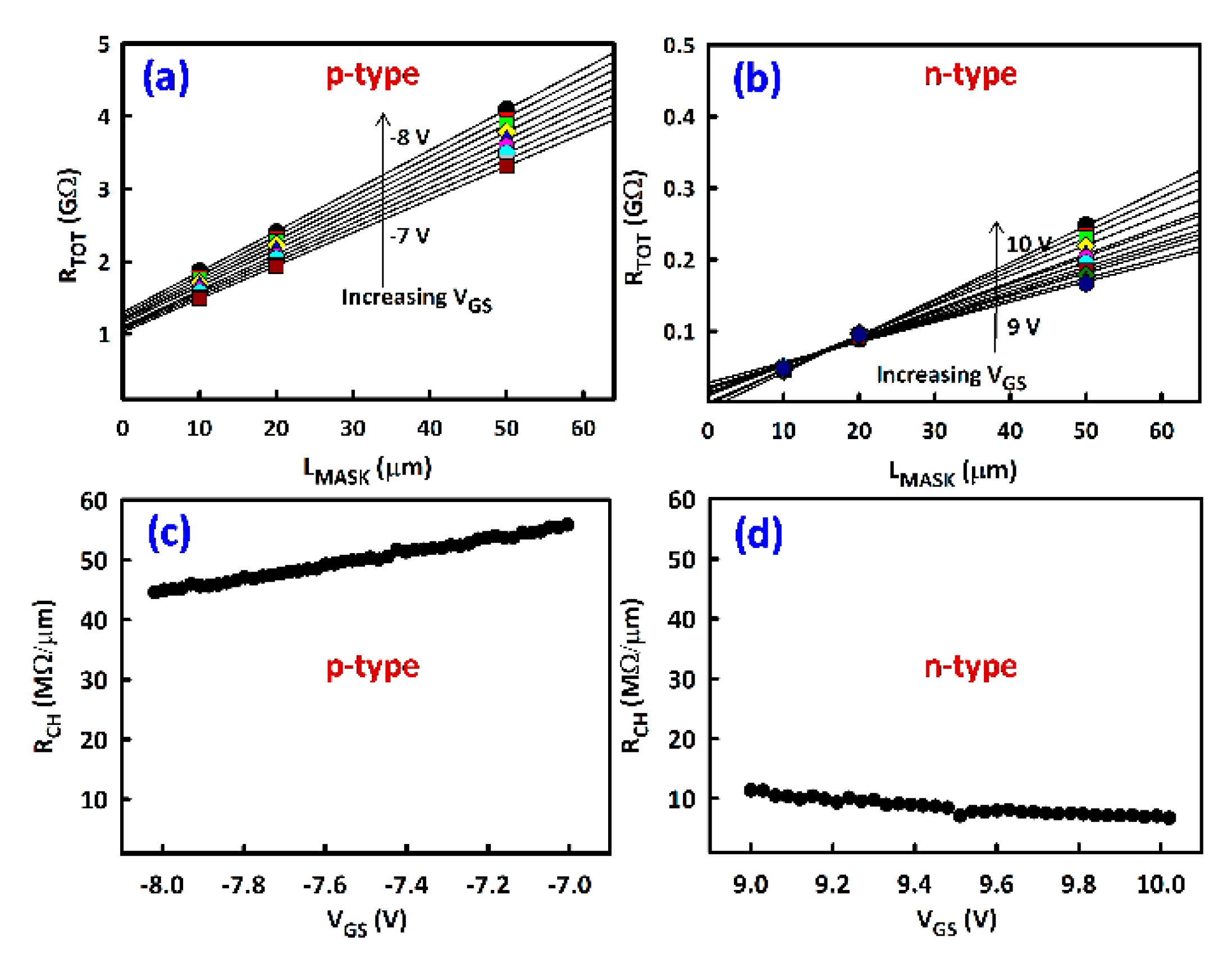
To separate the contact resistance (RCON) from the channel resistance (RCH), we used the “channel resistance” method [45]. In this method, it is assumed that the overall device resistance (RTOT = VDS/ID) is given by the sum of the effective channel resistance, RCH*LEFF, and RCON. RCH is supposed to be gate modulated, while RCON and LEFF (the effective L) are assumed to be independent from the VGS, such that the overall resistance is given by RTOT (VGS) = RCH (VGS)*LEFF + RCON. For a given VGS, using the linear least-squares method, it is possible to determine RCH(VGS) by fitting RTOT against LMASK, as shown in Figure 11a,b). The gradient gives the RCH at each VGS (Figure 11c,d).
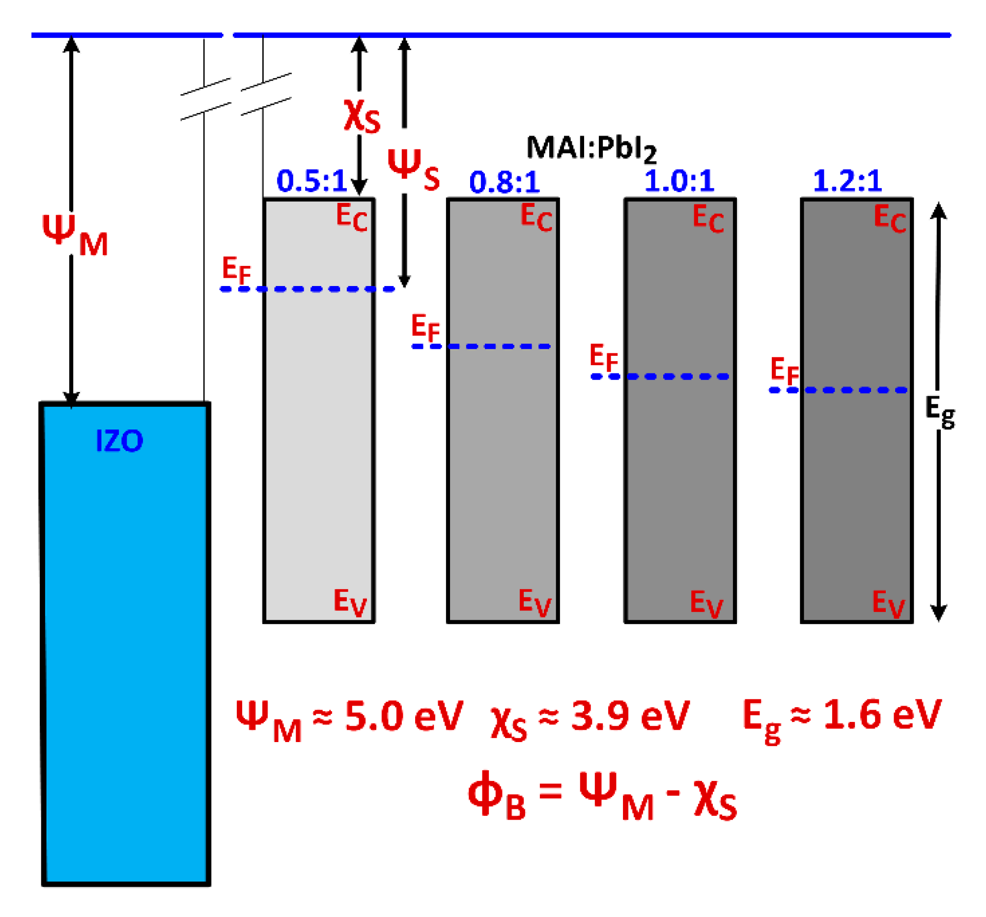
The RCH ranges from 5–11 and 44–55 MΩ/μm, respectively for the electron and hole transport (Figure 11c,d). The RCON is approximated to be 59 and 245 MΩ, respectively for the electron and hole transport. The large RCON, low ON state current and low μFE exhibited by these TFTs could be related to the existence of an injection barrier (ϕB) at the S/D-to-MAPbI3 contact (schottky contact) (Figure 12). A consequent of this is the current crowding that occurs in the output characteristics of the TFTs (Figure 6). Consistent with previous reports [30], the effect of the MAI/PbI2 ratio on the electrical properties of the TFTs indicate a shifting of the Fermi level (EF) towards the valence band (EV) with increasing MAI/PbI2 ratio (Figure 12). For MAI/PbI2 = 0.5, for instance, the film is n-type but highly resistive because of the excess PbI2. Furthermore, the IZO-MAPbI3 contact is schottky, given that ѰM is much larger than ѰS. On the other hand, the film processed with MAI/PbI2 = 1.2 is almost p-type but the contact in also schottky, given that ѰM should be much larger than ѰS to achieve an ohmic contact for hole transport (Figure 12).
The larger RCON for hole, as opposed to electron transport, corresponds to a larger voltage drop at the S/D-to-MAPbI3 contact, which may be the reason for the lower ON state current and the smaller μFE values. The large RCON is the reason for the strong dependency of the μFE on L for the hole transport (Figure 9a). A possible origin for the large variation in the other TFT parameters (Figure 9) could be ion migration in the MAPbI3 film [44]. As ion migration causes hysteresis in the current-voltage characteristics, the extracted TFT parameters may vary depending on the bias history of the devices. In addition, the devices presented herein do not have a passivation layer to protect the MAPbI3 film from environmental contamination. The variation in extracted parameters could thus be due to environmental changes. However, it is interesting to see that the TFTs are stable and work very well in ambient air, despite the absence of a passivation layer.
It is also important to note that the achievement of an ohmic contact for one carrier type consequently achieves a schottky contact for the other, given that ohmic contacts are achieved with a high metal workfunction for the hole transport and a low metal workfunction for the electron transport. Another important factor to consider for the ambipolar transport of the TFTs is the initial position of the EF, which may be determined by the MAI/PbI2 ratio and fabrication process conditions (Figure 12). Variation in carrier concentration by varying the precursor ratio have also been previously reported [30]. Therefore, balanced carrier transport may be achieved by varying the precursor ratio and by proper source/drain electrode selection for each carrier type.
5. Conclusions
The MAPbI3 TFTs investigated herein exhibited ambipolar transport, where simultaneous or selective transport of electrons and/or holes was possible in a single device, depending on the applied bias. However, the electron transport (n-type) was slightly more pronounced than the hole transport (p-type), and the on-state current of the n-type and p-type TFTs was highest in the slightly PbI2-rich and MAI-rich films, respectively, suggesting controllable n-type or p-type transport by precursor ratio. Furthermore, the use of different types of source/drain electrodes for each carrier type is necessary to balance the ambipolar transport.
6. Patents
CMOS DEVICE USING AMBIPOLAR ORGANIC-INORGANIC HYBRID PEROVSKITE AND METHOD OF MANUFACTURING THE SAME.
Author Contributions
Methodology, N.T.T.H.; investigation, J.J.; data curation, F.H.; writing—original draft preparation, J.J.; writing—review and editing, M.M.; supervision, M.M.
Funding
This research was funded by the National Research Foundation of South Korea (NRF) through the Korean Government (MSIP) under Grant NRF-2019R1F1A1059601 and Grant NRF-2018M3A9E9024942.
Acknowledgments
We would like to thank Jin Jang and Ravindra Bukke for their support in fabricating the devices and Jehwang Ryu, Amar Gupta, and Jongmin Lim for their support in taking the SEM images.
Conflicts of Interest
The authors declare no conflict of interest. The funders had no role in the design of the study; in the collection, analyses, or interpretation of data; in the writing of the manuscript, or in the decision to publish the results.
References
- Chen, Q.; De Marco, N.; Yang, Y.M.; Song, T.B.; Chen, C.C.; Zhao, H.; Yang, Y. Under the spotlight: The organic–inorganic hybrid halide perovskite for optoelectronic applications. Nano Today 2015, 10, 355–396. [Google Scholar] [CrossRef]
- Chin, X.Y.; Cortecchia, D.; Yin, J.; Bruno, A.; Soci, C. Lead iodide perovskite light-emitting field-effect transistor. Nat. Commun. 2015, 6, 7383. [Google Scholar] [CrossRef] [PubMed]
- Lee, M.M.; Teuscher, J.; Miyasaka, T.; Murakami, T.N.; Snaith, H.J. Efficient hybrid solar cells based on meso-superstructured organometal halide perovskites. Science 2012, 338, 643–647. [Google Scholar] [CrossRef] [PubMed]
- Ling, H.; Liu, S.; Zheng, Z.; Yan, F. Organic Flexible Electronics. Small Methods 2018, 2, 1800070. [Google Scholar] [CrossRef]
- Polman, A.; Knight, M.; Garnett, E.C.; Ehrler, B.; Sinke, W.C. Photovoltaic materials: Present efficiencies and future challenges. Science 2016, 352, aad4424. [Google Scholar] [CrossRef] [PubMed]
- He, Y.; Galli, G. Perovskites for solar thermoelectric applications: A first principle study of CH3NH3AI3 (A = Pb and Sn). Chem. Mater. 2014, 26, 5394–5400. [Google Scholar] [CrossRef]
- Chen, W.; Wu, Y.; Yue, Y.; Liu, J.; Zhang, W.; Yang, X.; Chen, H.; Bi, E.; Ashraful, I.; Grätzel, M.; et al. Efficient and stable large-area perovskite solar cells with inorganic charge extraction layers. Science 2015, 350, 944–948. [Google Scholar] [CrossRef] [Green Version]
- Cho, H.; Jeong, S.-H.; Park, M.-H.; Kim, Y.-H.; Wolf, C.; Lee, C.-L.; Heo, J.H.; Sadhanala, A.; Myoung, N.; Yoo, S.; et al. Overcoming the electroluminescence efficiency limitations of perovskite light-emitting diodes. Science 2015, 350, 1222–1225. [Google Scholar] [CrossRef]
- Deschler, F.; Price, M.; Pathak, S.; Klintberg, L.E.; Jarausch, D.-D.; Higler, R.; Hüttner, S.; Leijtens, T.; Stranks, S.D.; Snaith, H.J.; et al. High photoluminescence efficiency and optically pumped lasing in solution-processed mixed halide perovskite semiconductors. J. Phys. Chem. Lett. 2014, 5, 1421–1426. [Google Scholar] [CrossRef]
- Zhu, H.; Fu, Y.; Meng, F.; Wu, X.; Gong, Z.; Ding, Q.; Gustafsson, M.V.; Trinh, M.T.; Jin, S.; Zhu, X.-Y. Lead halide perovskite nanowire lasers with low lasing thresholds and high quality factors. Nat. Mater. 2015, 14, 636–642. [Google Scholar] [CrossRef]
- Stranks, S.D.; Snaith, H.J. Metal-halide perovskites for photovoltaic and light-emitting devices. Nat. Nanotechnol. 2015, 10, 391–402. [Google Scholar] [CrossRef] [PubMed]
- Sadhanala, A.; Deschler, F.; Thomas, T.H.; Dutton, S.E.; Goedel, K.C.; Hanusch, F.C.; Lai, M.L.; Steiner, U.; Bein, T.; Docampo, P.; et al. Preparation of single-phase films of CH3NH3Pb (I1–xBrx) 3 with sharp optical band edges. J. Phys. Chem. Lett. 2014, 5, 2501–2505. [Google Scholar] [CrossRef] [PubMed]
- Shi, D.; Adinolfi, V.; Comin, R.; Yuan, M.; Alarousu, E.; Buin, A.; Chen, Y.; Hoogland, S.; Rothenberger, A.; Katsiev, K.; et al. Low trap-state density and long carrier diffusion in organolead trihalide perovskite single crystals. Science 2015, 347, 519–522. [Google Scholar] [CrossRef] [PubMed] [Green Version]
- Sadhanala, A.; Ahmad, S.; Zhao, B.; Giesbrecht, N.; Pearce, P.M.; Deschler, F.; Hoye, R.L.Z.; Gödel, K.C.; Bein, T.; Docampo, P.; et al. Blue-green color tunable solution processable organolead chloride–bromide mixed halide perovskites for optoelectronic applications. Nano Lett. 2015, 15, 6095–6101. [Google Scholar] [CrossRef] [PubMed]
- Tan, Z.-K.; Moghaddam, R.S.; Lai, M.L.; Docampo, P.; Higler, R.; Deschler, F.; Price, M.; Sadhanala, A.; Pazos, L.M.; Credgington, D.; et al. Bright light-emitting diodes based on organometal halide perovskite. Nat. Nanotechnol. 2014, 9, 687–692. [Google Scholar] [CrossRef]
- Klauk, H. Organic thin-film transistors. Chem. Soc. Rev. 2010, 39, 2643–2666. [Google Scholar] [CrossRef]
- Wu, Y.; Li, J.; Xu, J.; Du, Y.; Huang, L.; Ni, J.; Cai, H.; Zhang, J. Organic–inorganic hybrid CH3NH3PbI3 perovskite materials as channels in thin-film field-effect transistors. RSC Adv. 2016, 6, 16243–16249. [Google Scholar] [CrossRef]
- Ngai, J.H.L.; Ho, J.K.W.; Chan, R.K.H.; Cheung, S.H.; Leung, L.M.; So, S.K. Growth, characterization, and thin film transistor application of CH3NH3PbI3 perovskite on polymeric gate dielectric layers. RSC Adv. 2017, 7, 49353–49360. [Google Scholar] [CrossRef]
- Xu, J.; Li, J.; Tang, L.; Peng, Y.; Wu, Y.; Du, Y.; Huang, L.; Ni, J.; Cai, H.; Zhang, J. The optimization of organic–inorganic perovskite films by annealing atmosphere for applications in transistors. Phys. Status Solidi 2017, 214, 1700170. [Google Scholar] [CrossRef]
- Peng, Y.; Tang, L.; Zhou, Z.; Xu, J.; Li, J.; Cai, H.; Ni, J.; Zhang, J. Enhancing perovskite TFTs performance by optimizing the interface characteristics of metal/semiconductor contact. J. Phys. D Appl. Phys. 2018, 51, 445101. [Google Scholar] [CrossRef]
- Tang, L.; Peng, Y.; Zhou, Z.; Wu, Y.; Xu, J.; Li, J.; Du, Y.; Huang, L.; Cai, H.; Ni, J.; et al. High-performance organic–inorganic hybrid perovskite thin-film field-effect transistors. Appl. Phys. A 2018, 124, 624. [Google Scholar] [CrossRef]
- Baikie, T.; Fang, Y.; Kadro, J.M.; Schreyer, M.; Wei, F.; Mhaisalkar, S.G.; Grätzel, M.; White, T.J. Synthesis and crystal chemistry of the hybrid perovskite (CH3NH3) PbI3 for solid-state sensitised solar cell applications. J. Mater. Chem. A 2013, 1, 5628–5641. [Google Scholar] [CrossRef]
- Yamada, Y.; Nakamura, T.; Endo, M.; Wakamiya, A.; Kanemitsu, Y. Near-band-edge optical responses of solution-processed organic–inorganic hybrid perovskite CH3NH3PbI3 on mesoporous TiO2 electrodes. Appl. Phys. Express 2014, 7, 032302. [Google Scholar] [CrossRef]
- Fang, H.-H.; Raissa, R.; Abdu-Aguye, M.; Adjokats, S.; Blake, G.R.; Even, J.; Loi, M.A. Photophysics of Organic–Inorganic Hybrid Lead Iodide Perovskite Single Crystals. Adv. Funct. Mater. 2015, 25, 2378. [Google Scholar] [CrossRef]
- Oga, H.; Saeki, A.; Ogomi, Y.; Hayase, S.; Seki, S. Improved Understanding of the Electronic and Energetic Landscapes of Perovskite Solar Cells: High Local Charge Carrier Mobility, Reduced Recombination, and Extremely Shallow Traps. J. Am. Chem. Soc. 2014, 136, 13818–13825. [Google Scholar] [CrossRef]
- Savenije, T.J.; Ponseca, C.S.; Kunneman, L.; Abdellah, M.; Zheng, K.; Tia, Y.; Zhu, Q.; Canton, S.E.; Scheblykin, I.G.; Pullerits, T.; et al. Thermally Activated Exciton Dissociation and Recombination Control the Carrier Dynamics in Organometal Halide Perovskite. J. Phys. Chem. Lett. 2014, 5, 2189–2194. [Google Scholar] [CrossRef] [Green Version]
- Wehrenfennig, C.; Liu, M.; Snaith, H.J.; Johnston, M.B.; Herz, L.M. Charge-carrier dynamics in vapour-deposited films of the organolead halide perovskite CH3NH3PbI3−xClx. Energy Environ. Sci. 2014, 7, 2269–2275. [Google Scholar] [CrossRef]
- Noh, J.H.; Im, S.H.; Heo, J.H.; Mandal, T.N.; Seok, S.I. Chemical management for colorful, efficient, and stable inorganic–organic hybrid nanostructured solar cells. Nano Lett. 2013, 13, 1764–1769. [Google Scholar] [CrossRef]
- Capelli, R.; Toffanin, S.; Generali, G.; Usta, H.; Facchetti, A.; Muccini, M. Organic light-emitting transistors with an efficiency that outperforms the equivalent light-emitting diodes. Nat. Mater. 2010, 9, 496–503. [Google Scholar] [CrossRef]
- Wang, Q.; Shao, Y.; Xie, H.; Lyu, L.; Liu, X.; Gao, Y.; Huang, J. Qualifying composition dependent p and n self-doping in CH3NH3PbI3. Appl. Phys. Lett. 2014, 105, 163508. [Google Scholar] [CrossRef]
- Senanayak, S.P.; Yang, B.; Thomas, T.H.; Giesbrecht, N.; Huang, W.; Gann, E.; Nair, B.; Goedel1, K.; Guha, S.; Moya, X.; et al. Understanding charge transport in lead iodide perovskite thin-film field-effect transistors. Sci. Adv. 2017, 3, e1601935. [Google Scholar] [CrossRef] [PubMed]
- Hoang, N.T.T.; Haque, F.; Ji, J.; Mativenga, M. Fast-Switching Mixed A-Cation Organic-Inorganic Hybrid Perovskite TFTs. IEEE Electron Device Lett. 2019, 40, 917–920. [Google Scholar] [CrossRef]
- Yusoff, A.R.B.M.; Kim, H.P.; Li, X.; Kim, J.; Jang, J.; Nazeeruddin, M.K. Ambipolar Triple Cation Perovskite Field Effect Transistors and Inverters. Adv. Mater. 2016, 29, 1602940. [Google Scholar] [CrossRef]
- Cheng, Y.; So, F.; Tsang, S.-W. Progress in air-processed perovskite solar cells: From crystallization to photovoltaic performance. Mater. Horiz. 2019, 6, 1611–1624. [Google Scholar] [CrossRef]
- Chen, Q.; Zhou, H.; Hong, Z.; Luo, S.; Duan, H.-S.; Wang, H.-H.; Liu, Y.; Li, G.; Yang, Y. Planar Heterojunction Perovskite Solar Cells via Vapor-Assisted Solution Process. J. Am. Chem. Soc. 2014, 136, 622–625. [Google Scholar] [CrossRef]
- Xiao, M.; Huang, F.; Huang, W.; Dkhissi, Y.; Zhu, Y.; Etheridge, J.; Gray-Weale, A.; Bach, U.; Cheng, Y.-B.; Spiccia, L. A Fast Deposition-Crystallization Procedure for Highly Efficient Lead Iodide Perovskite Thin-Film Solar Cells. Angew. Chem. Int. Ed. 2014, 53, 9898–9903. [Google Scholar] [CrossRef]
- Burschka, J.; Pellet, N.; Moon, S.-J.; Humphry-Baker, R.; Gao, P.; Nazeeruddin, M.K.; Gratzel, M. Sequential deposition as a route to high-performance perovskite-sensitized solar cells. Nature 2013, 499, 316–319. [Google Scholar] [CrossRef]
- Long, M.; Zhang, T.; Chai, Y.; Ng, C.-F.; Mak, T.C.W.; Xu, J.; Yan, K. Nanstoichiometric acid-base reaction as reliable synthetic route to highly stable CH3NH3PbI3 perovskite film. Nat. Com. 2016, 7, 13503. [Google Scholar] [CrossRef]
- Luo, S.; Daoud, W.A. Crystal Structure Formation of CH3NH3PbI3-xClx Perovskite. Materials 2016, 9, 123. [Google Scholar] [CrossRef]
- Ball, J.M.; Lee, M.M.; Hey, A.; Snaith, H.J. Low-temperature processed meso-superstructured to thin-film perovskite solar cells. Energy Environ. Sci. 2013, 6, 1739–1743. [Google Scholar] [CrossRef]
- Wang, B.; Huang, W.; Chi, L.; Al-Hashimi, M.; Marks, T.J.; Facchetti, A. High-k Gate Dielectrics for Emerging Flexible and Stretchable Electronics. Chem. Rev. 2018, 118, 5690–5754. [Google Scholar] [CrossRef] [PubMed]
- Meggiolaro, D.; Mosconi, E.; Angelis, F.D. Mechanism of Reversible Trap Passivation by Molecular Oxygen in Lead-Halide Perovskites. ACS Energy Lett. 2017, 2, 2794–2798. [Google Scholar] [CrossRef]
- Lu, D.; Zhang, Y.; Lai, M.; Lee, A.; Xie, C.; Lin, J.; Lei, T.; Lin, Z.; Kley, C.S.; Huang, J.; et al. Giant Light-Emission Enhancement in Lead Halide Perovskite by Surface Oxygen Passivation. Nano Lett. 2018, 18, 6967–6973. [Google Scholar] [CrossRef] [PubMed]
- Haque, F.; Hoang, N.T.T.; Ji, J.; Mativenga, M. Effect of Precursor Composition on Ion Migration in Hybrid Perovskite TFTs. IEEE Electron Device Lett. 2019. [Google Scholar] [CrossRef]
- Bhattacharya, P.; Bari, M.; Rao, K. Comparison of measurement techniques for gate shortening in sub-micrometer metal oxide semiconductor field effect transistors. Jpn. J. Appl. Phys. 1993, 32, 3409–3413. [Google Scholar] [CrossRef]
Figure 1.
Schematic cross-section of the MAPbI3 thin-film transistors (TFTs). During spin coating, the MAPbI3 sink into holes (“banks”) formed in the photoresist (PR) layer. The source (S) and drain (D) electrodes are made of indium zinc oxide (IZO) and the gate insulator is AlOx.
Figure 1.
Schematic cross-section of the MAPbI3 thin-film transistors (TFTs). During spin coating, the MAPbI3 sink into holes (“banks”) formed in the photoresist (PR) layer. The source (S) and drain (D) electrodes are made of indium zinc oxide (IZO) and the gate insulator is AlOx.

Figure 2.
Scanning electron microscope (SEM) images of 10 μm and 1 μm magnification of MAPbI3 films with varying MAI/PbI2 ratios of (a,b) 0.5, (c,d) 0.8, (e,f) 1, and (g,h) 1.2.
Figure 2.
Scanning electron microscope (SEM) images of 10 μm and 1 μm magnification of MAPbI3 films with varying MAI/PbI2 ratios of (a,b) 0.5, (c,d) 0.8, (e,f) 1, and (g,h) 1.2.

Figure 3.
X-ray diffraction (XRD) patterns of MAPbI3 films of varying MAI/PbI2 ratio.

Figure 4.
Atomic force microscope (AFM) images of the (a) AlOx and (b) MAPbI3 layer (MAI/PbI2 = 1.0) solution processed in ambient air.
Figure 4.
Atomic force microscope (AFM) images of the (a) AlOx and (b) MAPbI3 layer (MAI/PbI2 = 1.0) solution processed in ambient air.

Figure 5.
(a) XRD patterns of the solution processed AlOx layer as deposited (top), and after 350 °C annealing (bottom). (b) XPS spectra of the solution processed AlOx layer after annealing at 350 °C. Current–voltage (J–V) characteristics of the AlOx layer showing a breakdown voltage of approximately 4 MV/cm.

Figure 6.
P-type and n-type output characteristics (ID vs. VDS plots) of a MAPbI3 TFTs with MAI/PbI2 ratio of (a,b) 0.5, (c,d) 0.8, (e,f) 1.0, and (g,h) 1.2. W = 100 µm and L = 50 µm.
Figure 6.
P-type and n-type output characteristics (ID vs. VDS plots) of a MAPbI3 TFTs with MAI/PbI2 ratio of (a,b) 0.5, (c,d) 0.8, (e,f) 1.0, and (g,h) 1.2. W = 100 µm and L = 50 µm.

Figure 7.
Effect of bias in the ambipolar MAPbI3 TFTs.

Figure 8.
P-type and n-type transfer characteristics (log|ID| vs. VGS plots) of a MAPbI3 TFTs with MAI/PbI2 ratio of (a,b) 0.5, (c,d) 0.8, (e,f) 1.0, and (g,h) 1.2. W = 100 µm and L = 50 µm.
Figure 8.
P-type and n-type transfer characteristics (log|ID| vs. VGS plots) of a MAPbI3 TFTs with MAI/PbI2 ratio of (a,b) 0.5, (c,d) 0.8, (e,f) 1.0, and (g,h) 1.2. W = 100 µm and L = 50 µm.

Figure 9.
Extracted TFT parameters. (a–c) P-type and (d–f) n-type.

Figure 10.
Transfer characteristics (log |ID| vs VGS) and IG curves for TFTs with a channel width (W) of 100 µm and varying channel length (L). (a) The p-type and (b) n-type bias conditions. MAI/PbI2 = 1.2.
Figure 10.
Transfer characteristics (log |ID| vs VGS) and IG curves for TFTs with a channel width (W) of 100 µm and varying channel length (L). (a) The p-type and (b) n-type bias conditions. MAI/PbI2 = 1.2.

Figure 11.
Extraction of channel resistance (RCH). (a,b) Linear regression of the TFT’s total resistance (RTOT = VDS/ID), as a function of the design channel length (LMASK) for (a) p-type, and (b) n-type characteristics. (c,d) RCH per micrometer (of L) as a function of LMASK for (c) p-type and (d) n-type characteristics.

Figure 12.
Band diagrams for the IZO and MAPbI3 films of varying MAI/PbI2 ratio. ψm, ψs, χs, and Eg are the metal (IZO) workfunction, semiconductor (MAPbI3) workfunction, electron affinity of the MAPbI3, and band gap of the MAPbI3, respectively.
Figure 12.
Band diagrams for the IZO and MAPbI3 films of varying MAI/PbI2 ratio. ψm, ψs, χs, and Eg are the metal (IZO) workfunction, semiconductor (MAPbI3) workfunction, electron affinity of the MAPbI3, and band gap of the MAPbI3, respectively.

© 2019 by the authors. Licensee MDPI, Basel, Switzerland. This article is an open access article distributed under the terms and conditions of the Creative Commons Attribution (CC BY) license (http://creativecommons.org/licenses/by/4.0/).
Share and Cite
MDPI and ACS Style
Ji, J.; Haque, F.; Hoang, N.T.T.; Mativenga, M. Ambipolar Transport in Methylammonium Lead Iodide Thin Film Transistors. Crystals 2019, 9, 539. https://0-doi-org.brum.beds.ac.uk/10.3390/cryst9100539
AMA Style
Ji J, Haque F, Hoang NTT, Mativenga M. Ambipolar Transport in Methylammonium Lead Iodide Thin Film Transistors. Crystals. 2019; 9(10):539. https://0-doi-org.brum.beds.ac.uk/10.3390/cryst9100539
Chicago/Turabian StyleJi, Jeoungmin, Farjana Haque, Nhu Thi To Hoang, and Mallory Mativenga. 2019. "Ambipolar Transport in Methylammonium Lead Iodide Thin Film Transistors" Crystals 9, no. 10: 539. https://0-doi-org.brum.beds.ac.uk/10.3390/cryst9100539
Note that from the first issue of 2016, this journal uses article numbers instead of page numbers. See further details here.