Liquid Crystal-Based Enclosed Coplanar Waveguide Phase Shifter for 54–66 GHz Applications


1
Centre for Photonic Devices and Sensors, University of Cambridge, Cambridge CB3 0FA, UK
2
Department of Electrical and Electronic Engineering, Imperial College London, London SW7 2AZ, UK
*
Author to whom correspondence should be addressed.
Crystals 2019, 9(12), 650; https://0-doi-org.brum.beds.ac.uk/10.3390/cryst9120650
Submission received: 29 October 2019
/
Revised: 4 December 2019
/
Accepted: 4 December 2019
/
Published: 6 December 2019
(This article belongs to the Special Issue Microwave Liquid Crystal Technology)
Abstract
:A 0–10 V bias voltage-driven liquid crystal (LC) based 0°–180° continuously variable phase shifter was designed, fabricated, and measured with insertion loss less than −4 dB across the spectrum from 54 GHz to 66 GHz. The phase shifter was structured in an enclosed coplanar waveguide (ECPW) with LC as tunable dielectrics encapsulated by a unified ground plate in the design, which significantly reduced the instability due to floating effects and losses due to stray modes. By competing for spatial volume distribution of the millimeter-wave signal occupying lossy tunable dielectrics versus low-loss but non-tunable dielectrics, the ECPW’s geometry and materials are optimized to minimize the total of dielectric volumetric loss and metallic surface loss for a fixed phase-tuning range. The optimized LC-based ECPW was impedance matched with 1.85 mm connectors by the time domain reflectometry (TDR) method. Device fabrication featured the use of rolled annealed copper foil of lowest surface roughness with nickel-free gold-plating of optimal thickness. Measured from 54 GHz to 66 GHz, the phase shifter prototype presented a tangible improvement in phase shift effectiveness and signal-to-noise ratio, while exhibiting lower insertion and return losses, more ease of control, and high linearity as well as lower-cost fabrication as compared with up-to-date documentations targeting 60 GHz applications.
1. Introduction
Millimeter-wave phase shifters are of an ever-increasing research and development interest as vital components in phased array electronic beam steering systems, targeted 60 GHz high-data rate wireless communications [1], intersatellite communications, high-precision radar-based autonomous driving, hand-gesture sensing [2], and other forward-thinking applications. Existing microwave switchable techniques (e.g., radio frequency micro-electro-mechanical system (RF MEMS) and solid state p-i-n diodes) offer ultrafast but resolution-limited phase modulation due to their binary nature [3]. Continuous phase shifting can be realized by putting continuously tunable dielectrics in a guided structure to vary the wave speed. Nematic liquid crystals (LC) have been demonstrated with decent dielectric tunability and low dissipation factor particularly at millimeter-wavebands [4,5]. The dielectric tunability of LC is attributed to its molecular shape anisotropy and, hence, the dipole moment variation from the perpendicular state (⊥) to the parallel state (||) with an applied low-frequency bias field from below the Fredericks transition voltage to a saturated one. The variable polarization allows a continuous tuning of the dielectric constant and, hence, a differential phase shift when interacting with a millimeter-wave signal propagating over the delay line.
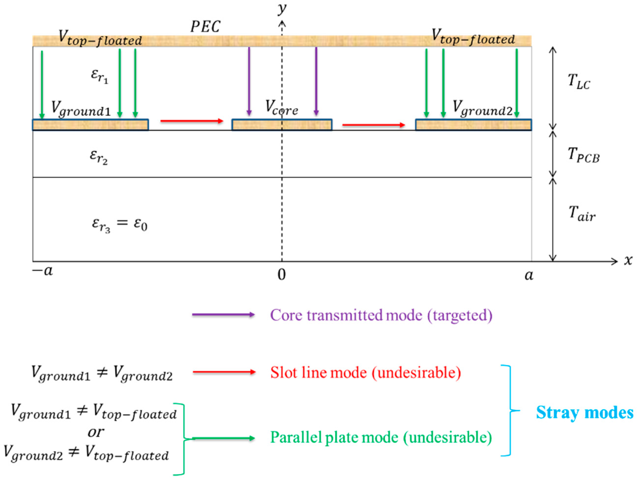
Extensive research attempts have been made on LC-based microwave technology [5,6,7,8,9,10], while rather less attention has been paid to the millimeter-wave applications with LC, challenged by the more stringent requirement regarding phase shifting range and resolution, insertion loss, operating bandwidth, linearity, signal-to-noise figure, power consumption, response time, robustness, size, large-scale integration, manufacturing tolerance, and cost, etc. We have explored the use of LC as low-loss tunable media for passive microwave analog components [11,12] and extended our phase shifter design into 60–90 GHz [3]. Different approaches of electrically-tunable device configurations combining with LC were studied for the millimeter-wavelength range, among which coplanar waveguide (CPW) was desirable as compared with other transmission lines [5,13,14] or waveguide structures [15,16,17,18] in terms of overall performance, ease of control, and circuit size. Specifically, conventional LC-based inverted microstrip line (IMSL) topology (well established below 30 GHz) struggles to target the 60 GHz band due to sharply increased insertion loss above 40 GHz, as evidenced in the phase shift-to-insertion loss ratio (figure-of-merit) compromising from 110°/dB at 24 GHz [13] to 20.8°/dB at 60.7 GHz [19] and 10°/dB at 66 GHz [5], respectively. Exploring into different aspects of the CPW approach, there are a host of variables and different configurations, but mainly divided into two groups, i.e., with or without a top-floating electrode (FE). Phase modulation of the FE-free CPW is entirely based on the two vertical slots instead of a planar cavity. We did a pilot study [3] on the tuning range limit of the FE-free CPW structure parameterized with geometrical aspect ratios and pointed out that such thin-Cu patterned structure suffers from low wave-occupied volume ratio of tunable LC to nontunable substrates, while a countermeasure we proposed using thick-Cu patterning and surface anchoring inside a deep channel challenged the status of precision manufacturing and LC alignment technology. Instead, the CPW-FE structure with a floating electrode on top [20,21,22,23] modulated the LC predominately at a planar cavity with the wave largely occupying tunable dielectrics, and, hence, reasonably higher tuning ranges and phase shifts were reported at microwave frequencies. A periodically loaded CPW-FE segments approach [24] reported a figure-of-merit of 60°/dB at 20 GHz with response times in the range of 110 ms–340 ms for LC layer thickness of 4 µm. However, CPW-FE was fundamentally narrowband and highly lossy at millimeter-wave frequencies due to the electric potential difference between coplanar grounds and the top electrode, producing stray modes (e.g., a slot line mode and a parallel plate mode as depicted in Figure 1) and even standing waves resonance that degraded the fundamental quasi-TEM mode transmission. In response to these limitations, this paper proposes a low-loss, broadband, and compact enclosed coplanar waveguide (ECPW) structure enabling 60 GHz applications based on a combination of LC and planar transmission line technologies, with a particular novelty on optimizing the tuning range and insertion losses by tailoring the spatial volume and distribution of millimeter-wave signal occupying tunable dielectrics versus nontunable dielectrics.
2. Materials and Methods
We propose a novel enclosed coplanar waveguide (ECPW) structure as shown in Figure 2 below, featuring a unified ground combining two coplanar ground planes with an enclosure engraved by electrical discharge machining (EDM). Compared with the conventional LC-based CPW-FE, the top conductor in our proposed ECPW structure was electrically shorted with the two coplanar grounds by continuous lateral sidewalls densely spaced within half a wavelength, which defined the electromagnetic boundary conditions for the tunable dielectrics (LC). The wide and flat enclosure-attached structure was envisaged to largely equalize the grounding electrodes’ electric potential for suppressing parasitic modes and the associated modes-coupling problems. Compared with traditional wire-bonded CPW implementation and grounded CPW (GCPW) by plated through-hole bias, our bias-free enclosure solution exhibited an improved grounding connectivity, lower insertion loss, and lower cost and enabled fast prototyping.
It remains a challenge to balance between insertion loss and phase-tuning range of a LC-based phase shifter for a reasonably good performance. The following methods are newly proposed to optimize our LC-based ECPW phase shifter design.
2.1. Bias Voltage-Dependent Impedance Matching
At different phase-shifting states, the characteristic impedance, reflection loss, and absorption loss of the phase shifter can change remarkably with the bias voltage due to the LC’s dielectric variations. At the voltage biasing state where the LC director field is perpendicular to the millimeter-wave polarization, the absorption loss tangent in LC was at a maximum, e.g., tanδ⊥ = 0.0123 ≫ tanδ∥ = 0.0032 at 60 GHz for the GT3-24002 (Merck) we used in this study. A particular novelty of this work is proposing a biasing-voltage dependent impedance-matching scenario to systematically reduce insertion loss, i.e., we strategically design the ECPW geometry to be of lowest reflection loss at the biasing state with maximal absorption losses. Thereby, adding up absorption and reflection losses, the total insertion loss was minimized. Furthermore, this method minimized insertion loss variation with bias voltages during 0–π continuous phase tuning, thereby minimizing the steering beam distortion without the need for tunable amplifiers or attenuators. This hugely reduced the system complexity and mitigated noise level introduced by the amplitude-compensating networks.
2.2. Tuning Range Ratio and Insertion Loss Analysis
Phase shift and insertion loss both closely connect with the dielectric constant ratio of tunable to nontunable media, i.e., in this study, as it determined spatial volume distribution of millimeter-wave electric flux in lossy but functional dielectrics (i.e., LC). Wave-occupied volume ratio (WoVR) is proposed in Equation (1) below for analyzing the effective dielectric constant () of the transmission line.
where WoVRk represents the electric flux ratio in the region k, the quantity of which hinges on dielectric constant of the region () and the conductors’ geometry. Based on this, the maximum obtainable differential phase shift is given by Equation (2), where f is the frequency of the millimeter-wave signal, L is the physical length of the phase shifter (tunable part), is the light velocity in vacuum, and denote the effective dielectric constant of the structure with LC biased by a saturated voltage, and a reference voltage (0 V in this study), respectively.
Combining Equations (1) and (2), increasing results in an elevated and thus an improved . Without loss of generality for a variety of LCs with different birefringence, we denote the maximum tuning range ratio (TRR) normalized to a specific type of LC as
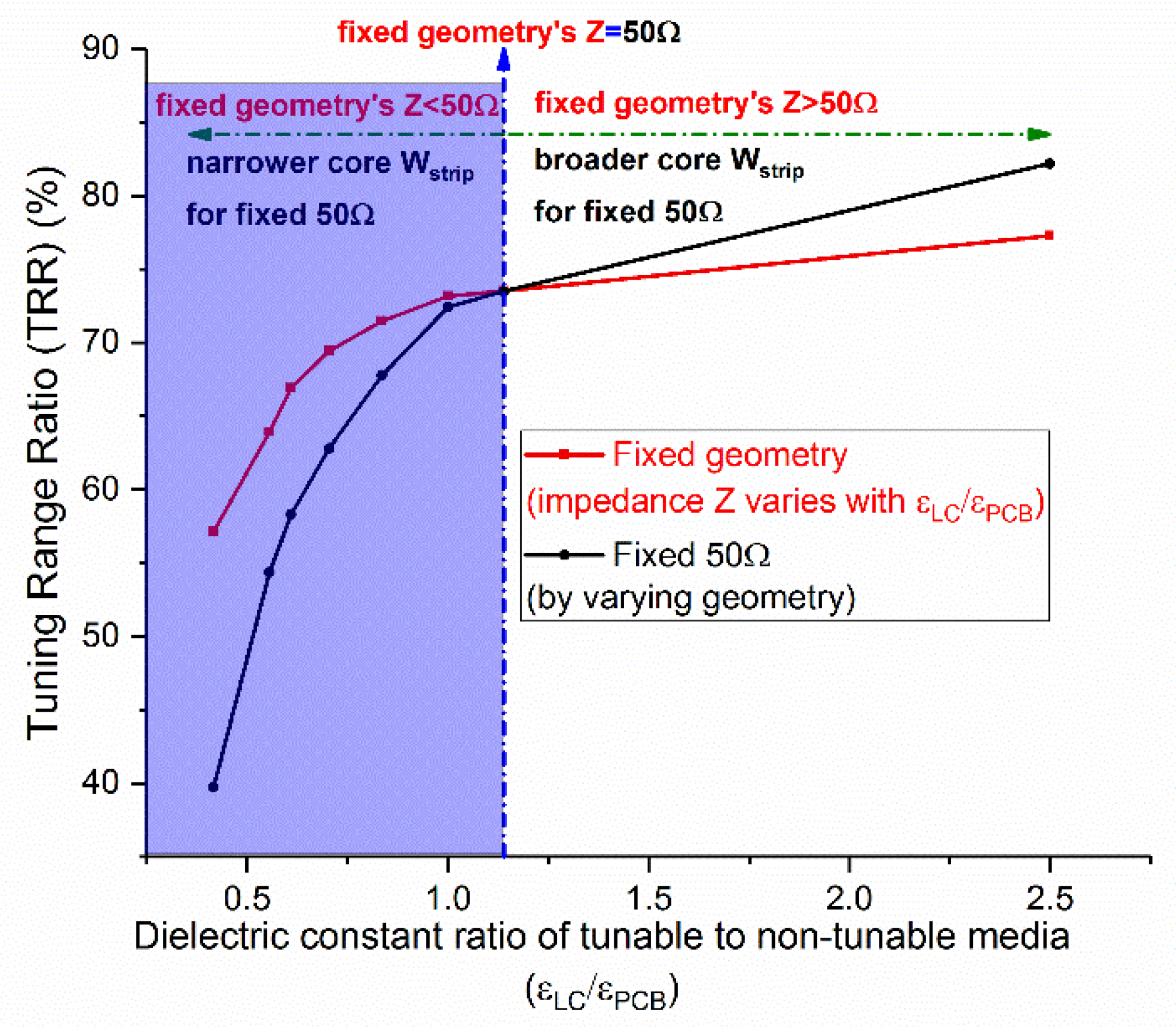
Note that LC’s dielectric constant ranges around 2.4 to 3.3 at microwave and millimeter-wave frequencies, thus a change of LC materials makes a limited difference to the WoVR as compared with that of nontunable print circuit board (PCB) substrates with ranging from 2.1 to 10.2 depending on material compositions (e.g., polytetrafluoroethylene (PTFE), ceramic, woven glass fiber). We firstly modeled an enclosed CPW (ECPW) with a fixed LC and a fixed LC-layer thickness , computing the maximum TRR parametrized with for the following two cases, i.e., a fixed geometry (with varied impedance), and a fixed impedance (by a varied geometry). By 66 GHz simulations using a 3D electromagnetic (EM) simulation software, ANSYS HFSS, we obtain in Figure 3 that TRR drops with the decrease of owing to the reduced . However, there was a slump in TRR in the case of the 50 Ω controlled-impedance requirement as compared with that in case of a fixed geometry, as illustrated in the area colored blue where the fixed geometry exhibited an impedance lower than 50 Ω.
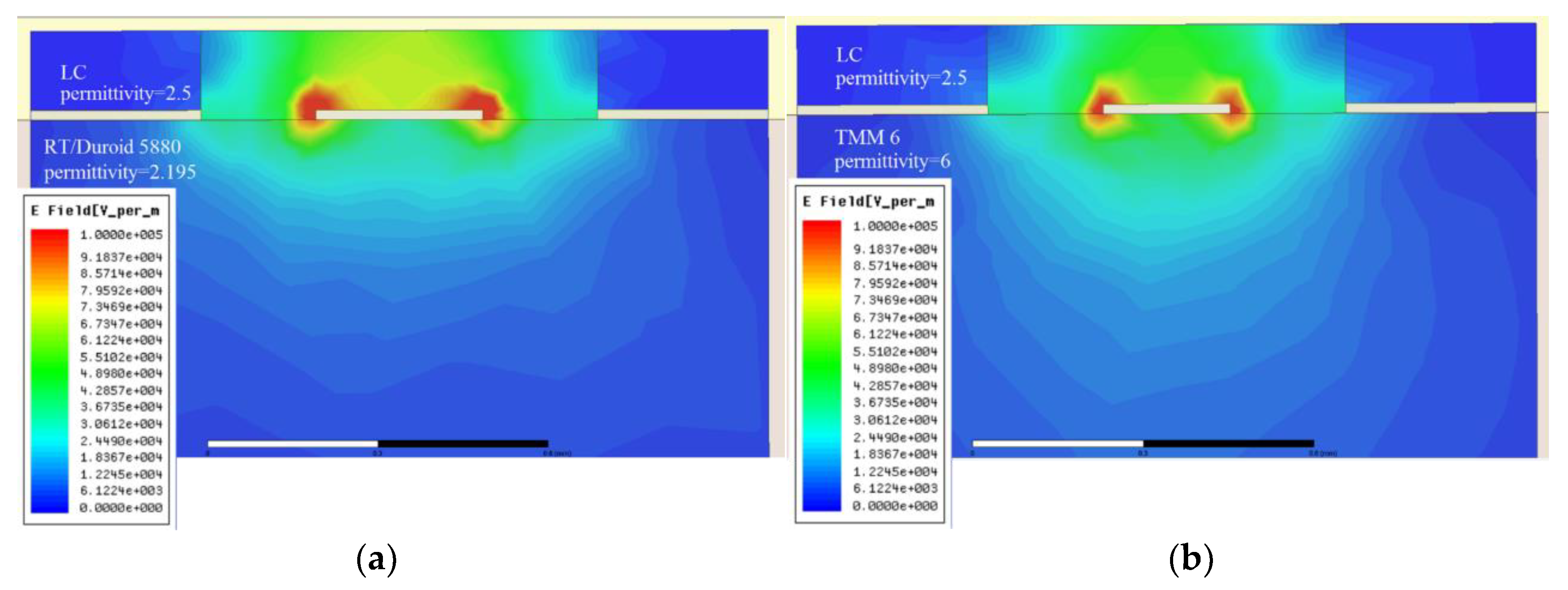
The enhanced nonlinearity observed in the fixed-impedance case is attributed to the core line’s geometrical variations, i.e., to maintain 50 Ω, the core line’s width, , narrowed with the decrease of . By way of illustration in Figure 4a,b below (with a same power input and a scale bar of the field intensity), the narrowing of the core reduced the further, which aggravated the nonlinearity as shown above in Figure 3, i.e., the TRR nonlinearity was a combined effect of the dielectric constant ratio () and the geometry. Arguably, the maximum TRR characterizes the geometrical coefficient of the tunable dielectrics, which positively correlated to the . Commercially available Roger’s RT/duroid 5880 or Taconic’s TLY-5 are theoretically the suitable PCB substrate candidates with dielectric constant ( = 2.195) at 54–66 GHz closest for the optimal dielectric constant ratio () based on the nematic LC we used, i.e., GT3-24002 (Merck) with 2.5 at 0 V bias, and 3.3 at saturated bias.
Based on the aspect ratios derived for 50 Ω impedance matching, the optimal thickness of the liquid crystal was searched for by looking into the minimum insertion loss while satisfying the phase shift requirement of π in this study. For a fixed geometry, the phase-tuning range and insertion loss both increased with , as observed. However, such increase was nonlinear in case of a controlled impedance because of the geometrical variation’s impact on The phase shift-to-loss optimization was performed in recognition of this nonlinearity. According to our previous work on loss derivation [3], the peak phasor forms of the LC volumetric loss per unit length at the 0 V biasing state, and the total metal core line loss (thickness considered) per unit length are given by Equations (4) and (5), respectively.
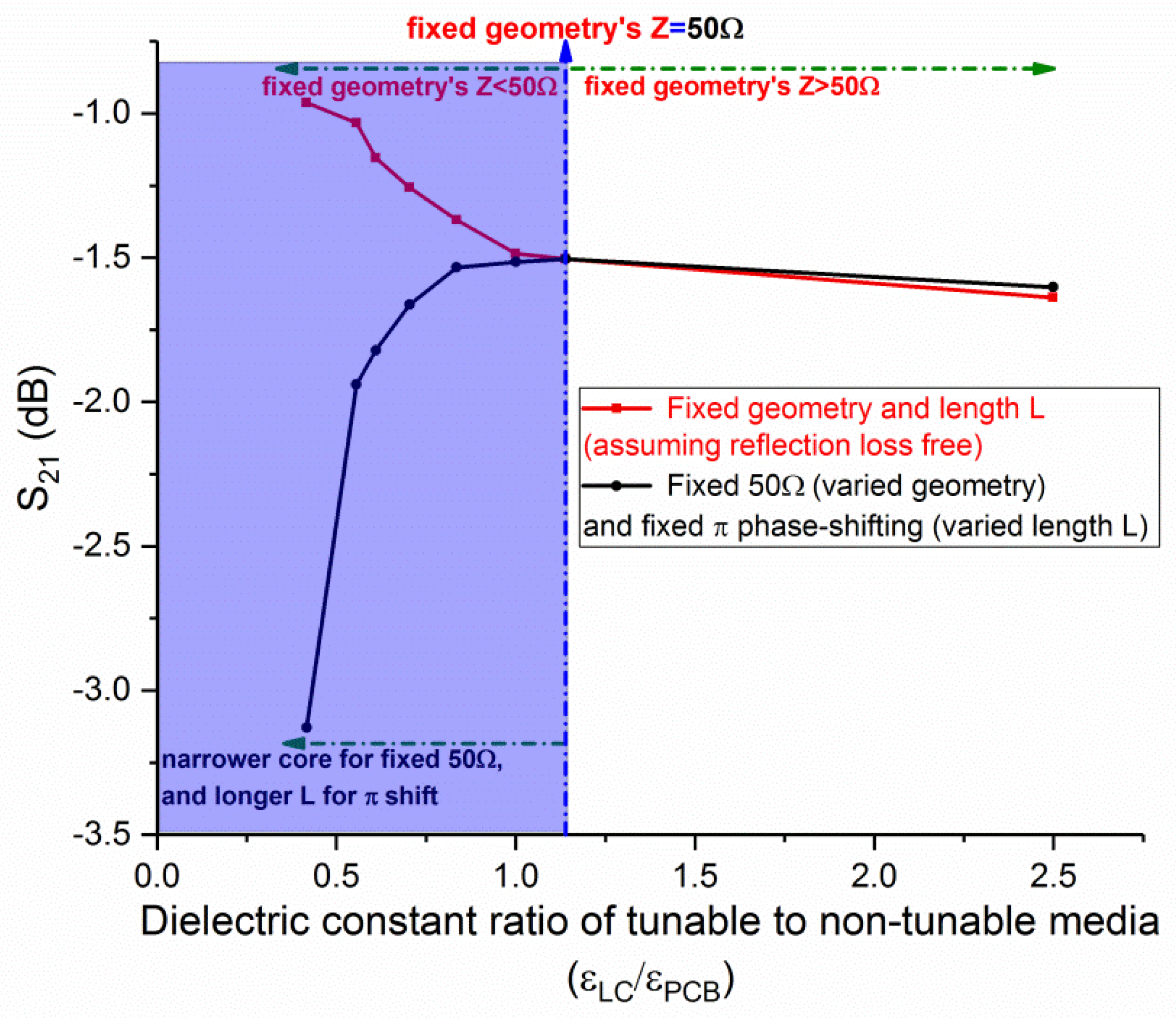
Based on this, we quantified the insertion loss in Figure 5 for the above parametric models. For the case of a fixed geometry and line length L, it was assumed that the loss calculation was not normalized to any controlled impedance, and thus the forward transmission obtained is free of return loss, i.e., only the materials’ absorption losses constituted the insertion loss. Note that at 66 GHz the PCB substrate was less lossy than LC as tan, thus the decrease of (i.e., a reduced ) resulted in an improved . However, for the case of a fixed 50 Ω (reflection-free) and a fixed phase shift, the slump in TRR required an increased length L to compensate for a fixed phase-shifting requirement (e.g., π), and, hence, a dramatic drop in was observed with the decrease of . The insertion loss nonlinearity was a joint effect of not only the dielectric constant ratio () and the cross-sectional geometry but also of the transmission line length (L).
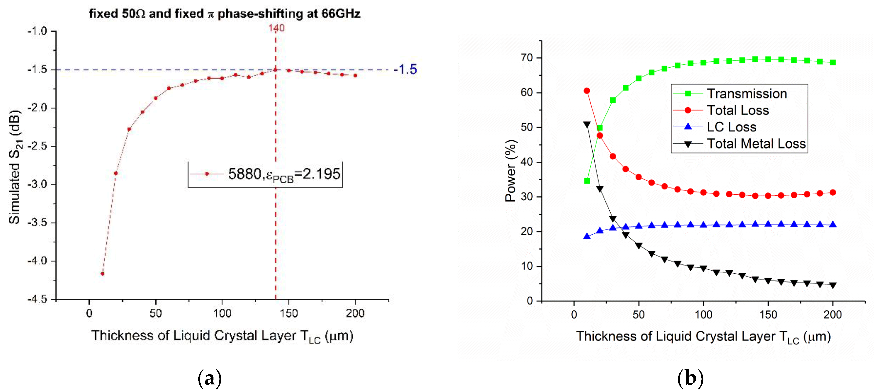
In awareness of the nonlinearities above for a fixed LC-layer thickness , we subsequently varied targeted for fixed 50 Ω and π shifting. Likewise, narrowed with the drop of the to keep 50 Ω. However, the closer proximity of core and top conductors resulted in an elevated electric field intensity especially around the core’s surface, hence, the domination of metal loss (see Figure 6b below), which contributed to a slump in as shown in Figure 6a. The ratio of the total conductor losses (assuming a perfectly smooth surface) to the total losses was quantified as parameterized with the LC thickness at 66 GHz. The simulation was performed in a 50 Ω controlled impedance (by varying and for each ) and for a fixed phase shifting of π (by varying the line length L).
It is worth noting the difference in the order of operations between Equations (4) and (5) regarding the derived material losses, i.e., squaring then integrating (for dielectric loss), versus the integrating first then squaring (for metal loss), which accounted for the different phenomena that metal loss and dielectric loss level off with , respectively, as illustrated in the almost constant LC loss level versus the change of , while the metal loss drops dramatically. Very few freedoms were envisaged to optimize the LC’s dielectric dissipation by changing the geometry, due to the limit of keeping the aspect ratio ( to ) for impedance matching. However, increasing the LC thickness played a dominant role in mitigating the conductor loss and, hence, reducing the total material absorption loss at 66 GHz, even without considering the metal surface roughness (which elevated the proportion of conductor loss further). Increasing the LC thickness from 10 μm to 100 μm, the conductor loss reduced from 51.1% to 9.6%, the total loss correspondingly dropped by 30%. Based on an optimal = 140 μm, the corresponding 50 Ω-optimized ECPW transmission line (with fabrication tolerances considered) was with a cross section of = 293 μm, = 203 μm, and a length L of 14.32 mm for a maximum differential phase shift of π at 66 GHz.
2.3. PCB-to-Connectors Interface Design by Time Domain Reflectometry
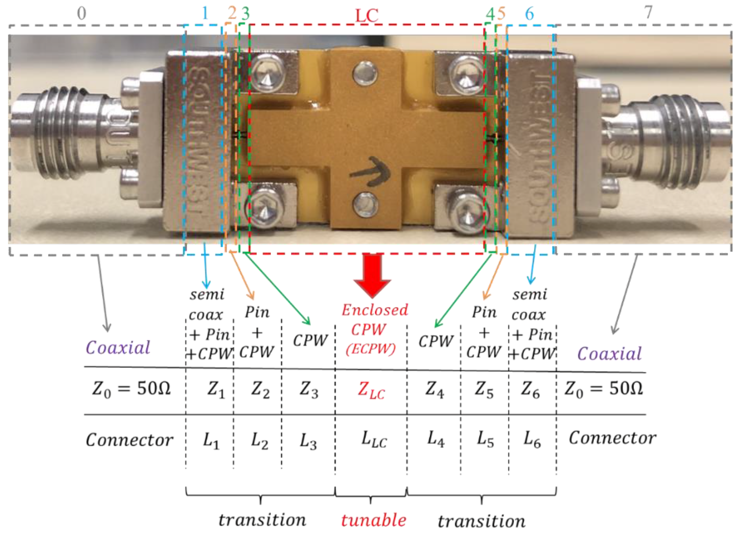
Interfaces between the optimized 50 Ω tunable ECPW and 50 Ω 1.85 mm coaxial connectors were not 50 Ω, owing to the change of polarization, hence the need for a transition design for the whole-device impedance matching and low-reflection signal transmission. The work itself was challenging because of the irregular nature of the connection region. Time domain reflectometry (TDR) method was employed to accurately characterize the transient impedance of the coaxial CPW ECPW interfaces.
From the wave-propagating point of view (longitudinal direction), configuration of the phase shifter device was divided into multiple cross-sections (Figure 7 below) with different propagation modes at the interface of each geometrical discontinuity, e.g., from coaxial to CPW to ECPW for the input, and vice versa for the output. To minimize losses due to reflection and higher-order modes radiation, the designed PCB’s edge patterns at these interfaces were sized with minimized diametrical discontinuities, which tailored smooth polarization transitions in different planes and produced tight transverse couplings.
3. Experiment and Results
3.1. Device Fabrication
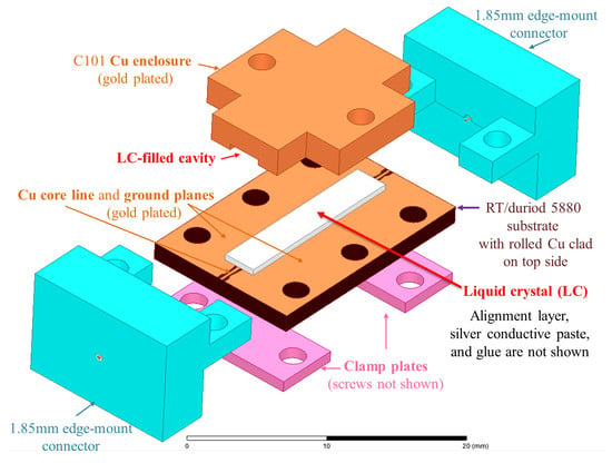
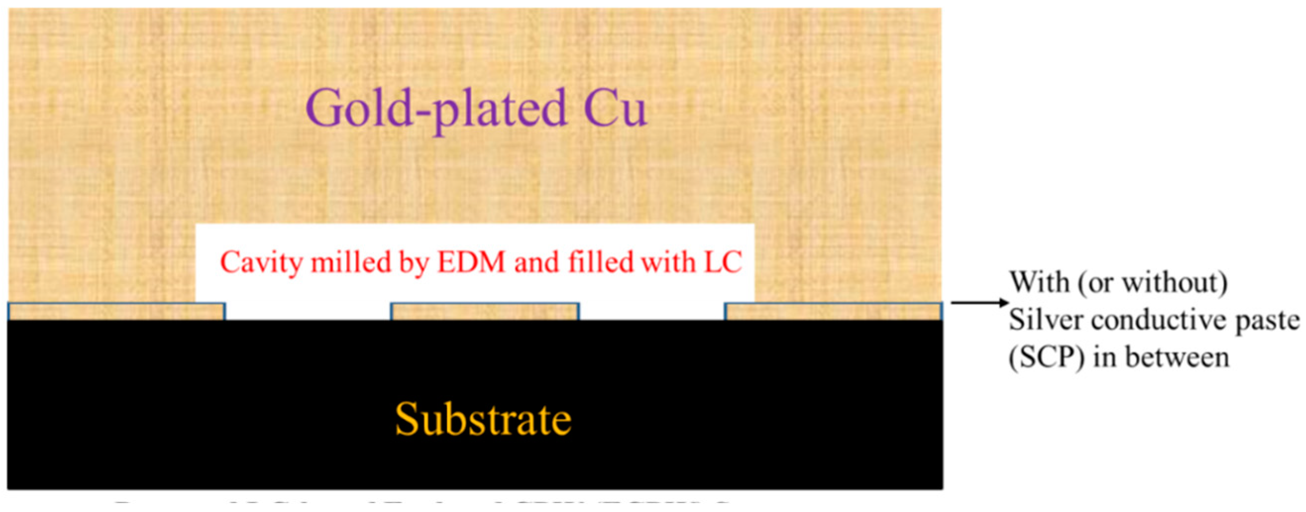
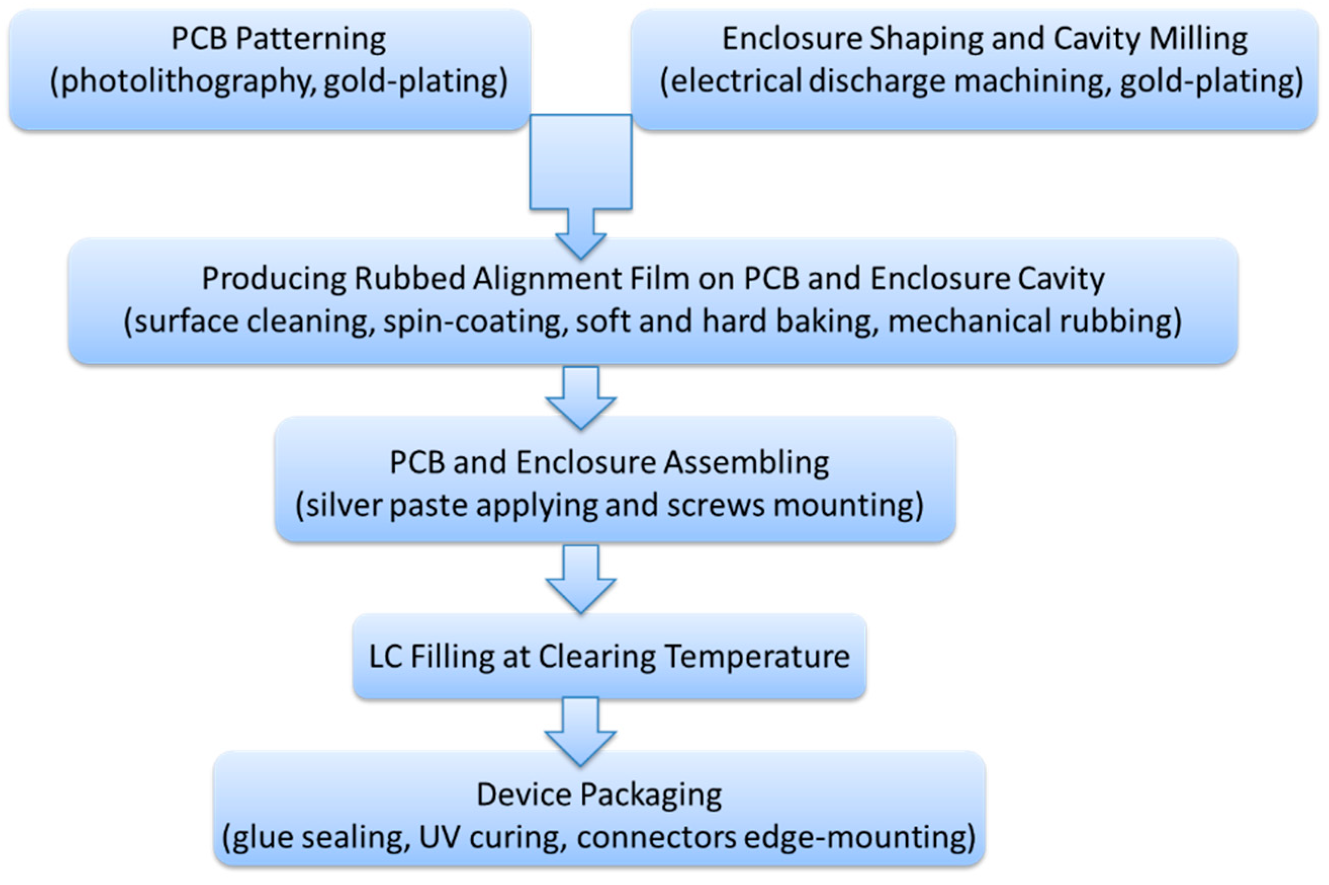
Prototyping process of the designed phase shifter is outlined in Figure 8. The proposed ECPW was patterned in two parts, i.e., a RT/duroid 5880 PCB substrate (with rolled annealed copper foil of lowest surface roughness to our knowledge) and an enclosure, which were then electrically joined by inverting the enclosure and attaching to the PCB. Sidewalls of the enclosed cavity eliminated spacers used in traditional LC-based IMSL structures, which provided improved uniformity of the LC layer and enabled fast prototyping. All the patterned conductors were gold-plated (nickel-free) in an optimal thickness of 2 μm by experiment for reliable protection against copper oxidation and the subsequent migration into gold after 200 °C baking (a process for evaporating the solvent of the coated alignment agent on the substrate). Silver conductive paste was then applied between the enclosure and the CPW’s ground planes for enhanced electric connectivity.
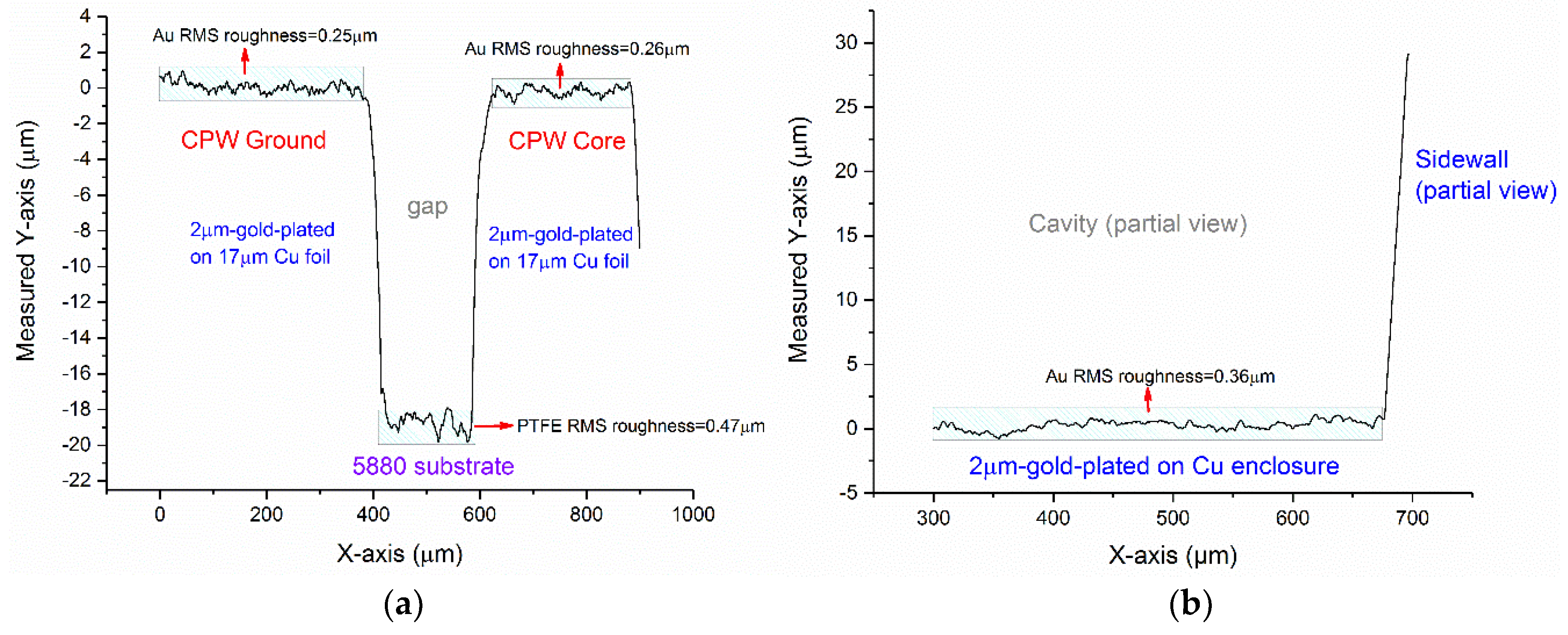
Cross-section profiles of the gold-plated conductors were measured using a Dektak profilometer (Veeco) with a stylus radius of 12.5 µm. Measured statistics are enclosed in Figure 9a for the CPW part, and Figure 9b for the enclosure. Standard deviation analysis showed that root-mean-square (RMS) roughness of the 2-µm thick gold-plating surface was 0.26 µm for the CPW core line, and 0.25 µm for the CPW ground plane, the smoothness of which outperformed most documentation with 0.4–0.5 µm reported.
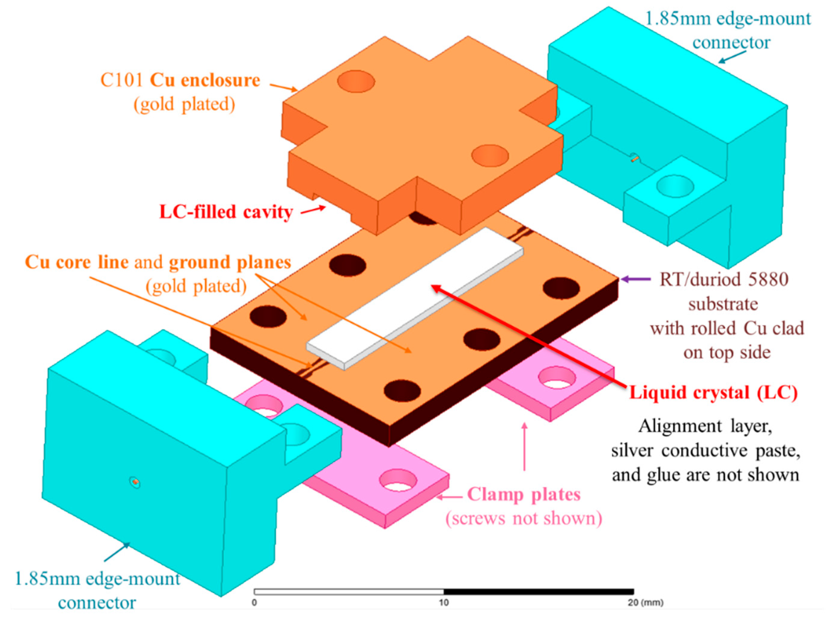
The patterned substrates were then coated with a planar alignment layer, i.e., Optmer AL1254 polyimide (JSR Micro), and mechanically rubbed to anchor LC for a targeted orientation. Compared with nylon solution, AL1254 is free of formic acid and hence eliminated the corrosion problem. Moreover, the processing time was significantly reduced from 3 h to less than 30 min, exhibiting two benefits. First, the much shorter baking time alleviated dimensional instability of substrates due to mismatch in coefficient of thermal expansion, hence mitigating a series of losses at millimeter-wave caused by this. Second, the decreased time needed for substrates processing allowed fast device prototyping. This benefit was noticeable, as the efficiency of the LC-based device assembling process was highly limited by the long baking time. Figure 10 below illustrates the components assembling process in four steps, i.e., PCB and enclosure screwing with silver conductive paste added, LC filling by a one-drop capillary method, followed by openings sealing, and finally connectors edge mounting.
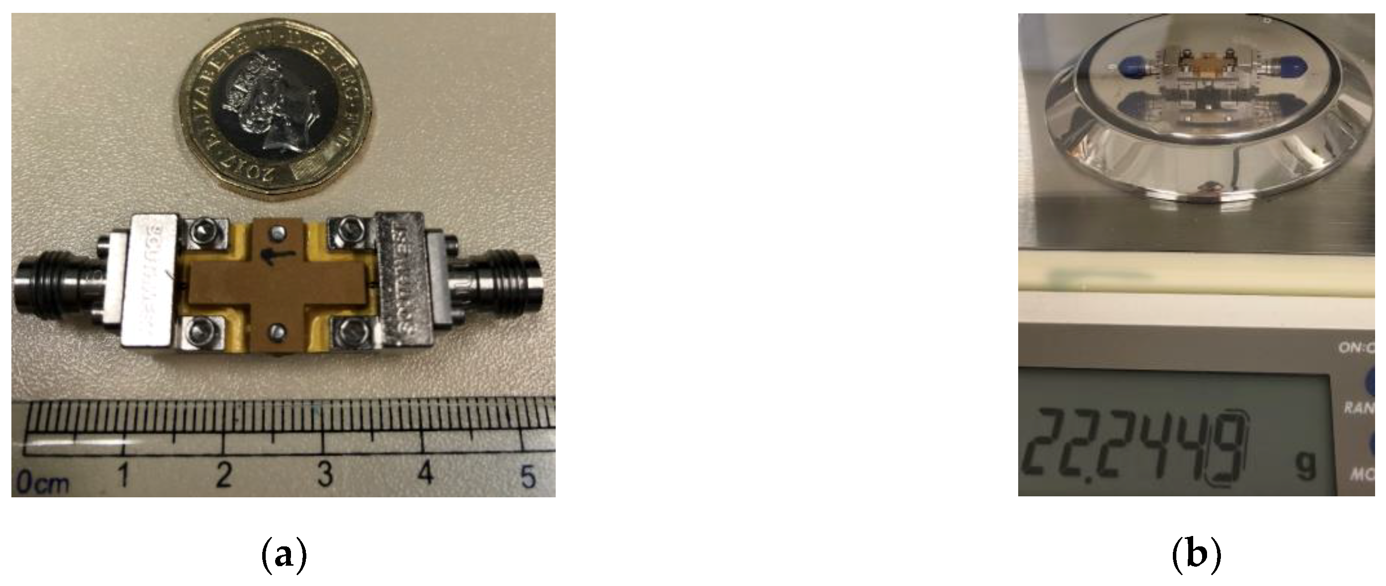
Scattering parameters were measured using R&S ZVA67, a two-port one-source vector network analyzer (Rohde & Schwarz) covering the useful 57–66 GHz unlicensed band designated for 5G communications in Europe. Two iterations of devices were fabricated to optimize the linear phase shift-voltage response, and mitigate parasitic resonance and pseudo rectangular waveguide modes, while compensating for the substrate’s stress relief and dimensional deformation. A final prototype is shown in Figure 11, with 5.2 cm in length and 22.2 g in weight including connectors.
3.2. Measurement Results and Device Optimization
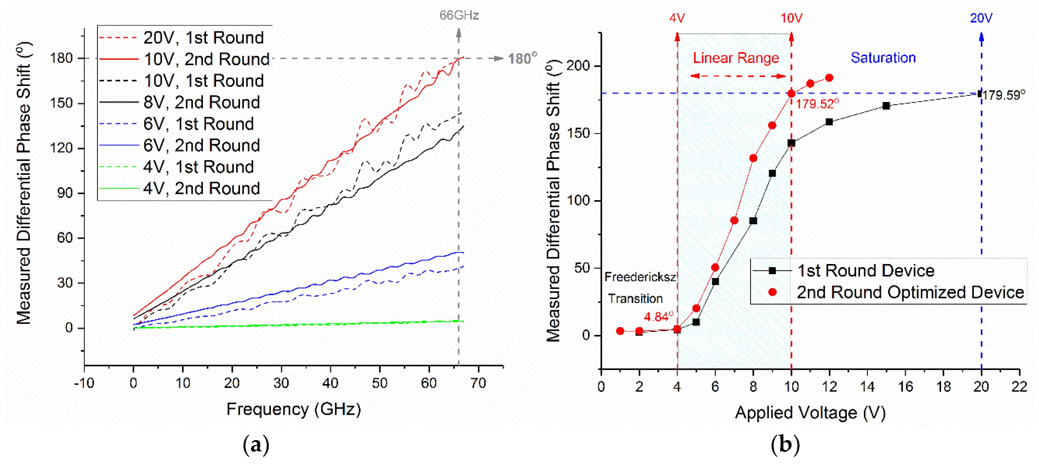
Differential phase shifts as a function of frequency and bias voltages were measured for devices of the first round and the second iteration designs. As demonstrated in Figure 12 below, a phase shift of π at 66 GHz was achieved with ease by a much lower biasing field of only up to 10 V for the second-round optimized device, as compared with the 20 V required by the first round. In Figure 12a, phase shift ripples in the spectrum were further mitigated through addressing the coefficient of thermal expansion mismatch and surface waves radiation. As evidenced by Figure 12b, the second-round device keeps a desirable feature of the first-round design, i.e., the linear response of differential phase shift vs. bias voltage from 5 V to 10 V for low-voltage control (≈0.1 V/μm). By extending the length of the tunable ECPW part but without altering the LC’s thickness (i.e., not changing the agility of field-dependent orientation variation), the bias voltage required for π shift was confirmed to decrease from 20 V to 10 V for ease of control and a reduced power consumption. The linear phase shift agility now covers a phase shift range from 4.8° to 179.5°, corresponding to a low-frequency voltage bias from 4 V to 10 V. The nonlinearities occurring below the Fredericks transition voltage (4 V) and above the saturation voltage (10 V) were of minor importance to the performance, as the linear range had covered most of the full phase tuning range (0–π).
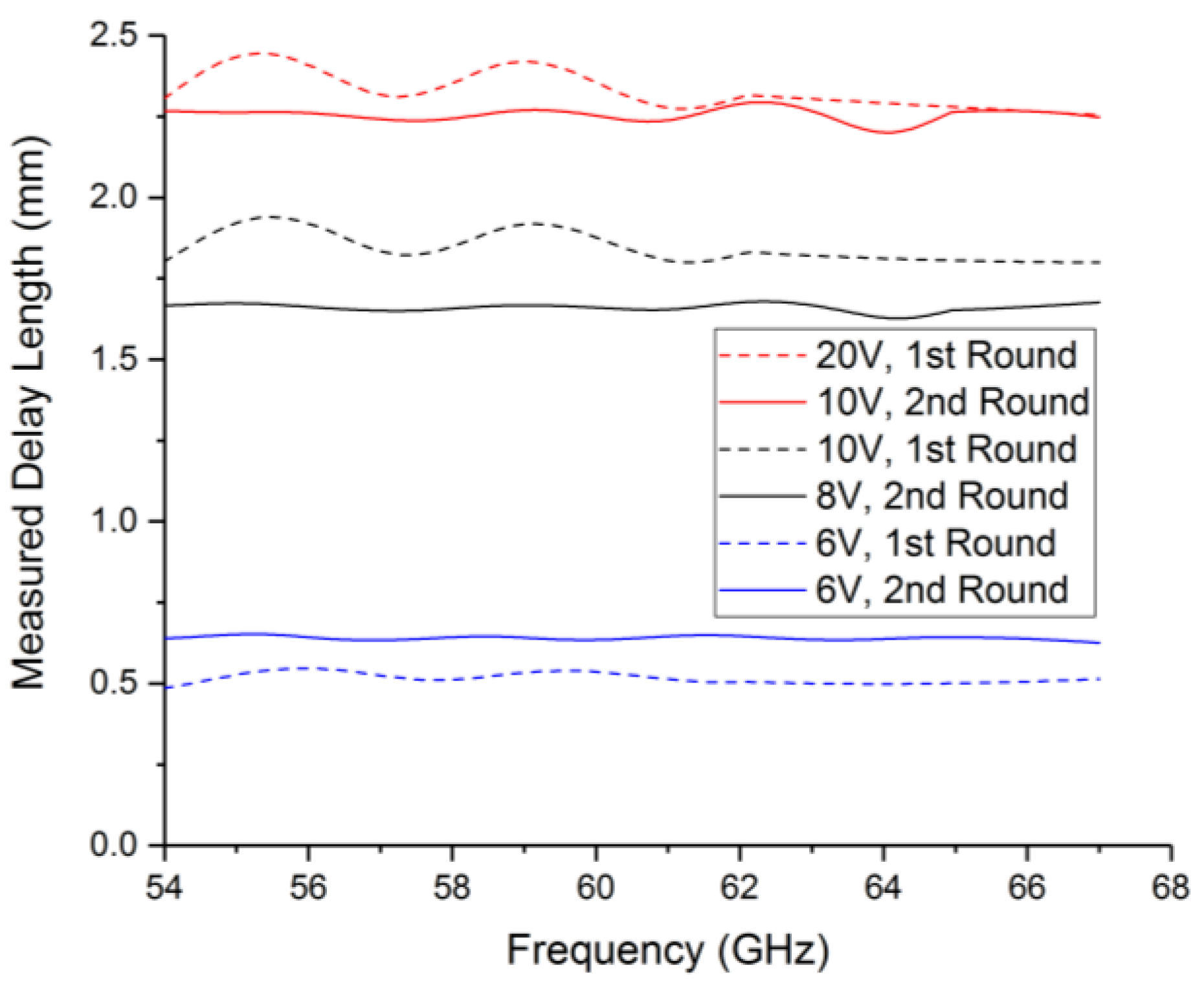
Based on the differential phase shift measured, delay length (in millimeter) is quantified in Figure 13 below. The delay produced by the optimized device (second round) exhibited frequency independence, indicating a highly desirable true time-delay property for ultra-wideband phased array antenna beam steering free of beam squinting.
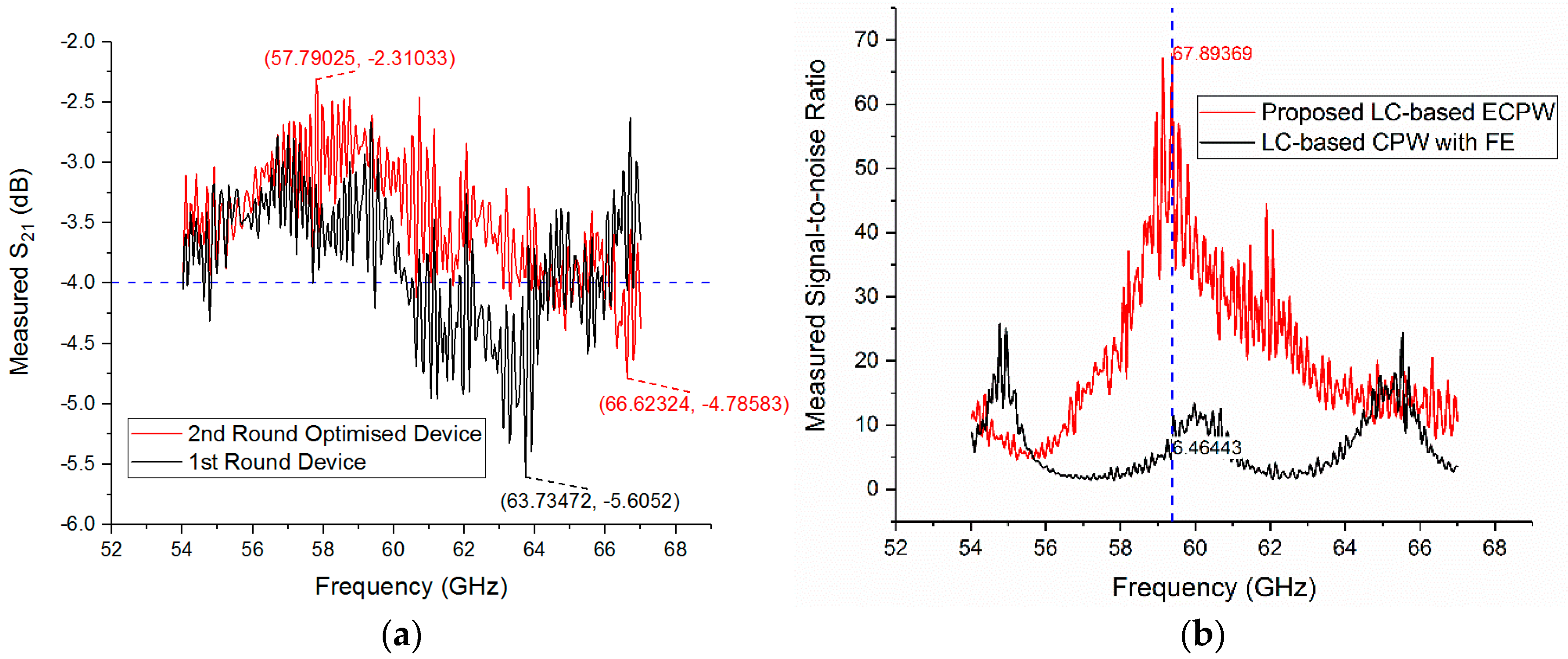
Measured insertion loss shown in Figure 14a below confirms that the narrowing of the cavity width (from 1.3 mm to 1 mm) compared with wavelength accounted for the insertion loss dip-free spectrum broadening, with the single mode upper operation frequency (limited by the onset of waveguide modes and the associated surface wave coupling) pushed from 64 GHz to above 66 GHz. Signal-to-noise ratios were measured for fabricated LC-based phase shifters designed in the proposed ECPW structure, as well as one based on a conventional CPW-FE configuration. The measurement results compared in Figure 14b demonstrates a broadband improvement in the signal-to-noise ratio from 57 GHz to 66 GHz, as the proposed ECPW structure including an enclosed ground in the design appreciably reduced the instability due to the floating effect in a multiconductor transmission line.
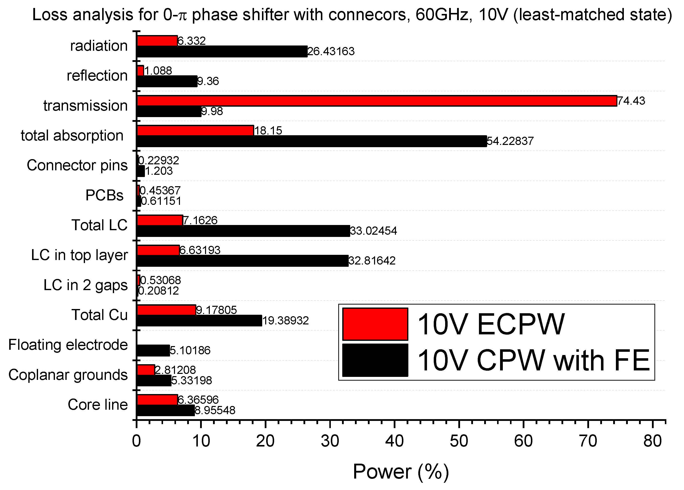
Further analysis was performed by a loss decomposition simulation at 60 GHz, concerning the power percentage of signal transmission, signal reflection (due to mismatching and higher-order modes), material absorptions by dielectrics and metals (including energy from the fundamental mode, as well as the stray modes), higher-order modes, and surface wave radiation into the free space. As summarized in Figure 15 below, the proposed ECPW achieved suppression of higher-order spurious modes radiation by 20% and reduced LC absorption loss by 26% due to the elimination of extra dissipations introduced by the higher-order modes. For the similar reason, the total metal loss also decreased by 10%. Return loss dropped by 8%, and, in total, insertion loss reduced by 65%.
Transient performance of the LC-based ECPW phase shifter was assessed by measuring the response time under various voltages biases, with the results ranging from 4 s (rise time with 10 V bias applied) to 12 s (fall time once removal of bias), with minor dependence on the millimeter-wave spectrum (identical switching speed for 54 GHz and 67 GHz signal), as the LC orientation was attributed to the change of low frequency electric field intensity only.
4. Discussion
Measured performance of the optimized LC-based ECPW phase shifter at 66 GHz was compared with up-to-date documentations covering state-of-the-art millimeter-wave phase shifters realized in a variety of technologies and structures. As listed in Table 1 below, the different technologies compared at a same frequency (66 GHz), our wideband (54–66 GHz) phase-shifting solution outperformed solid state technology in terms of lower insertion loss (−4 dB > −5.9 dB). Our modest loss solution was even as competitive as those state-of-the-art MEMS and magnetic-biased waveguides. Note that the results measured in other people’s work were predominately with on-wafer probe-based characterization setups (no connectors), under which case the insertion loss reported could be underestimated as compared with our connectors-embedded device.
Compared with our LC-based ECPW, the MEMS-based phase shifter [26] at 66 GHz exhibited a lower insertion loss (−2.7 dB > −4 dB) for a phase shift of π. However, the MEMS solution was inherently digital and, hence, resolution-limited when integrating in a beam steering system. Furthermore, the reliability and robustness merits further investigation for a clearer picture of its competitiveness over LC. Regarding LC-based waveguide technologies at 66 GHz, one of the ridged waveguide phase shifters [15] reported the highest phase shift and the highest phase shift-to-insertion loss ratio realized at the same time. The highly anisotropic LC material they deploy was MDA-03-2844 (Merck), with a 100 µm cell gap and a tunable length of 17 mm. However, the main disadvantage lies in its bulky and power-consuming magnetic biasing networks. Although the || state (LC director with respect to the millimeter-wave polarization) reported can be implemented by a 10 V driving, the ⊥ state cannot be realized without a strong magnetic field, which significantly limits its potential for applications requiring lightweight and low-power consumptions. Another ridged waveguide phase shifter [15] based on dual frequency switching LC MDA-05-1132 was reported with full-electric bias (free from magnets). However, the high insertion loss (−11 dB for 193° shift) and low figure-of-merit (17.5°/dB) impeded its deployment for low-loss applications.
The main drawback of our 0–10 V driven LC-based ECPW phase shifter lies in the tuning speed (4 s for switching on, 12 s for switching off). Regarding the quadratic dependence of the response time on the GT3-24002 LC thickness, we did not intend to reduce the LC thickness in this study for a faster response at a cost of degrading the desirable linearity of 0–π shift vs. 4–10 V bias, as well as increasing the material absorption and, hence, insertion loss due to elevated electric field intensity. Albeit struggling to meet the fast response requirement by automotive radars, our LC-based ECPW phase shifters can still be deployed advantageously at millimeter-wave as a static beam steering solution for applications where fast response is not a priority, e.g., satellite relay links (where the angular tracking requirement is typically 4°/min for a low earth-orbiting satellite tracking a geosynchronous satellite), weather radars, radio telescopes, etc.
5. Conclusions
This work contributed a passive millimeter-wave broadband (54–66 GHz) analogue phase shifter implemented in a liquid crystal-based enclosed coplanar waveguide (ECPW) structure which screened out interference and stray modes, allowing resonance-free quasi-TEM wave propagation from 54 GHz to 66 GHz. The structure not only retained the true-TEM advantage of the FE-free CPW we initially designed [3], but also achieved a high tuning range based on modulating a planar LC layer on top of the CPW’s core line in addition to the two CPW slots. More fundamentally, the continuous sidewalls of the enclosed cavity served as a unified grounding path to substantially address the stray modes and energy leakage problems posed by conventional CPW with floating electrodes. On this basis (i.e., a stray mode-free ECPW boundary condition), we optimized the tunable transmission line portion by competing for spatial volume distribution of the millimeter-wave signal occupying lossy tunable dielectrics (i.e., LC) versus low-loss but nontunable dielectrics (i.e., PTFE), and minimizing the total of dielectric volumetric loss and metal surface loss for a fixed phase-tuning range under a controlled impedance. For a fixed geometry, phase-tuning range and insertion loss both increased with dielectric constant ratio of LC to PCB substrate. However, such an increase was nonlinear in the case of a controlled impedance (e.g., 50 Ω) due to geometrical variation effects on the wave-occupied volume ratio. Phase shift to loss optimization was thereby performed in recognition of this nonlinearity. The fabricated device prototype outperformed other LC-based planar structures reported in terms of the measured phase shift-to-insertion loss ratio, signal-to-noise ratio, and linearity. An ease of control with a lower power consumption (0–10 V) and compact size was demonstrated as compared with LC-based waveguide solutions tuned by power-consuming and bulky magnets. Potentially, the proposed LC-based ECPW phase shifters are envisaged to be incorporated into a planar feeding network of a phased array antenna to develop compact beam-steering systems of improved performances targeted for ultra-high data rate wireless communications, intersatellite communications, and other smart devices such as hand gesture recognition sensors.
Author Contributions
Investigation, writing—original draft preparation, J.L.; supervision, conceptualization, writing—review and editing, D.C.
Funding
UK Engineering and Physical Sciences Research Council (EPSRC) through the EPSRC Centre for Doctoral Training in Integrated Photonic and Electronic Systems (EP/L015455/1).
Acknowledgments
The author would like to thank Kasia Surowiecka for the cleanroom training.
Conflicts of Interest
The authors declare no conflict of interest.
References
- Thomas, N.; Carlos, C.; Adriana, B.F.; Edward, W.K.; Eldad, P.; Joerg, W. IEEE 802.11ad: directional 60 GHz communication for multi-Gigabit-per-second Wi-Fi [Invited Paper]. IEEE Commun. Mag. 2014, 52, 132–141. [Google Scholar]
- Jaime, L.; Nicholas, G.; Emre, M.K.; Patrick, A. Soli: Ubiquitous gesture sensing with millimetre wave radar. ACM Trans. Graph. 2016, 35, 142. [Google Scholar]
- Li, J.F.; Xu, H.; Chu, D.P. Design of liquid crystal based coplanar waveguide tunable phase shifter with no floating electrodes for 60–90 GHz applications. In Proceedings of the 2016 46th European Microwave Conference (EuMC), London, UK, 4–6 October 2016; pp. 1047–1050. [Google Scholar]
- Lim, K.C.; Margerum, J.D.; Lackner, A.M. Liquid crystal millimetre wave electronic phase shifter. Appl. Phys. Lett. 1993, 75, 1065–1067. [Google Scholar] [CrossRef]
- Garbovskiy, Y.; Zagorodnii, V.; Krivosik, P.; Lovejoy, J.; Camley, R.E.; Celinski1, Z.; Glushchenko, A.; Dziaduszek, J.; Dąbrowski, R. Liquid crystal phase shifters at millimetre wave frequencies. J. Appl. Phys. 2012, 111, 054504. [Google Scholar] [CrossRef]
- Martin, N.; Laurent, P.; Prigent, G.; Philippe, G.; Fabrice, H. Technological evolution and performances improvements of a tunable phase-shifter using liquid crystal. Microw. Opt. Technol. Lett. 2004, 43, 338–341. [Google Scholar] [CrossRef]
- Zografopoulos, D.C.; Ferraro, A.; Beccherelli, R. Liquid-crystal high-frequency microwave technology: Materials and Characterization. Adv. Mater. Technol. 2019, 4, 1800447. [Google Scholar] [CrossRef]
- Holger, M.; Matthias, J.; Roland, R.; Ersin, P.; Matthias, N.; Rolf, J. Microwave liquid crystal technology. Crystals 2018, 8, 355. [Google Scholar] [CrossRef] [Green Version]
- Santi, C.P.; Enrica, M.; Francesco, C.; Matteo, A.; Stefano, M. Surface wave dispersion for a tunable grounded liquid crystal substrate without and with metasurface on top. IEEE Trans. Antennas Propag. 2017, 65, 3540–3548. [Google Scholar]
- Pouria, Y.; Onur, H.K.; Bevan, B.; Christophe, F.; Rolf, J. Electrically Tuned Microwave Devices Using Liquid Crystal Technology. Int. J. Antenn. Propag. 2013, 2013, 824214. [Google Scholar] [CrossRef] [Green Version]
- Longzhu, C.; Huan, X.; Jinfeng, L.; Daping, C. High Figure-of-merit compact phase shifters based on liquid crystal material for 1–10 GHz applications. Jpn. J. Appl. Phys. 2017, 56, 011701. [Google Scholar] [CrossRef]
- Longzhu, C.; Huan, X.; Jinfeng, L.; Daping, C. High FoM liquid crystal based microstrip phase shifter for phased array antennas. In Proceedings of the 2016 International Symposium on Antennas and Propagation (ISAP), Okinawa, Japan, 24–28 October 2016; pp. 402–403. [Google Scholar]
- Muller, S.; Scheele, P.; Weil, C.; Wittek, M.; Hock, C.; Jakoby, R. Tunable passive phase shifter for microwave applications using highly anisotropic liquid crystals. In Proceedings of the IEEE MTT-S International Microwave Symposium Digest, Fort Worth, TX, USA, 6–11 June 2004; pp. 1153–1156. [Google Scholar]
- Mueller, S.; Penirschke, A.; Damm, C.; Scheele, P.; Wittek, M.; Weil, C.; Jakoby, R. Broad-band microwave characterization of liquid crystals using a temperature-controlled coaxial transmission line. IEEE Trans. Microw. Theory Tech. 2005, 53, 1937–1945. [Google Scholar] [CrossRef]
- Stefan, M.; Felix, G.; Patrick, S.; Michael, W.; Christian, H.; Rolf, J. Passive phase shifter for W-band applications using liquid crystals. In Proceedings of the 2006 European Microwave Conference (EuMC), Manchester, UK, 10–15 September 2006; pp. 306–309. [Google Scholar]
- Gaebler, A.; Goelden, F.; Manabe, A.; Goebel, M.; Mueller, S.; Jakoby, R. Investigation of high performance transmission line phase shifters based on liquid crystal. In Proceedings of the 2009 European Microwave Conference (EuMC), Rome, Italy, 29 September–1 October 2009; pp. 594–597. [Google Scholar]
- Jost, M.; Weickhmann, C.; Strunck, S.; Gäbler, A.; Fritzsch, C.; Karabey, O.H.; Jakoby, R. Liquid crystal based low-loss phase shifter for W-band frequencies. Electron. Lett. 2013, 49, 1460–1462. [Google Scholar] [CrossRef]
- Wang, K.D.; Wu, K. Liquid crystal enabled substrate integrated waveguide variable phase shifter for millimetre-wave application at 60GHz and beyond. In Proceedings of the 2015 IEEE MTT-S International Microwave Symposium, Phoenix, AZ, USA, 17–22 May 2015; pp. 1–4. [Google Scholar]
- Bulja, S.; Mirshekar-Syahkal, D.; Yazdanpanahi, M.; James, R.; Day, S.E.; Fernández, F.A. Liquid Crystal Based Phase Shifters in 60 GHz Band. In Proceedings of the 3rd European Wireless Technology Conference, Paris, France, 27–28 September 2010; pp. 37–40. [Google Scholar]
- Sahbani, F.; Tentillier, N.; Legrand, C.; Karine, B. Coplanar liquid crystal reconfigurable phase-shifters. Mol. Cryst. Liq. Cryst. 2011, 542, 726. [Google Scholar] [CrossRef]
- Kamei, T.; Moritake, H.; Utsumi, Y. Microwave and light-wave measurements for nematic-liquid-crystal-loaded phase shifter using coplanar waveguide with floating electrode. Jpn. J. Appl. Phys. 2010, 49, 01AF03. [Google Scholar] [CrossRef]
- Nose, T.; Yanase, T.; Yanagihara, S.; Honma, M. Transmission properties of the coplanar waveguide type liquid crystal cell. In Proceedings of the 2005 Joint 30th International Conference on Infrared and Millimetre Waves and 13th International Conference on Terahertz Electronics, Williamsburg, VA, USA, 19–23 September 2005; pp. 567–568. [Google Scholar]
- Nose, T.; Yanagihara, S.; Honma, M. Operational mode of millimetre-wave phase shifter using liquid crystal materials with coplanar waveguide. Jpn. J. Appl. Phys. 2007, 46, 1114–1117. [Google Scholar] [CrossRef]
- Goelden, F.; Gaebler, A.; Goebel, M.; Manabe, A.; Mueller, S.; Jakoby, R. Tunable liquid crystal phase shifter for microwave frequencies. Electron. Lett. 2009, 45, 686–687. [Google Scholar] [CrossRef]
- Ku, B.H.; Schmalenberg, P.; Inac, O.; Gurbuz, O.D.; Lee, J.S.; Shiozaki, K.; Rebeiz, G.M. A 77–81-GHz 16-element phased-array receiver with 50 beam scanning for advanced automotive radars. IEEE Trans. Microw. Theory Tech. 2014, 62, 2823–2832. [Google Scholar] [CrossRef]
- Kim, H.T.; Park, J.H.; Lee, S.; Kim, S.; Kim, J.M.; Kim, Y.K.; Kwon, Y. V-band 2-b and 4-b low-loss and low-voltage distributed MEMS digital phase shifter using metal-air-metal capacitors. IEEE Trans. Microw. Theory Tech. 2002, 50, 2918–2923. [Google Scholar]
- Carsten, F.; Flavio, G.; Onur, H.K.; Saygin, B.; Sabrina, C.; Rolf, J. Advanced characterisation of a W-band phase shifter based on liquid crystals and MEMS technology. Int. J. Microw. Wirel. Technol. 2012, 4, 379–386. [Google Scholar]
Figure 1.
Stray modes in a liquid crystal (LC)-based coplanar waveguide (CPW) with floating electrodes (CPW-FE).
Figure 1.
Stray modes in a liquid crystal (LC)-based coplanar waveguide (CPW) with floating electrodes (CPW-FE).

Figure 2.
Proposed LC-filled enclosed coplanar waveguide (ECPW) structure (cross section).

Figure 3.
Simulated maximum tuning range ratio (TRR) of the LC-based ECPW at 66 GHz: Fixed geometry with varied impedances vs. fixed 50 Ω with varied geometries.
Figure 3.
Simulated maximum tuning range ratio (TRR) of the LC-based ECPW at 66 GHz: Fixed geometry with varied impedances vs. fixed 50 Ω with varied geometries.

Figure 4.
Simulated 66 GHz electric field intensity distribution in a LC-based ECPW with materials of different dielectric constant ratios (a) = 1.14, (b) = 0.42 (both with 0V bias, power input = 1W at 66GHz, varied geometries for a fixed 50 Ω).
Figure 4.
Simulated 66 GHz electric field intensity distribution in a LC-based ECPW with materials of different dielectric constant ratios (a) = 1.14, (b) = 0.42 (both with 0V bias, power input = 1W at 66GHz, varied geometries for a fixed 50 Ω).

Figure 5.
Simulated at 66 GHz (0 V bias) for two cases: Fixed geometry with varied impedances vs. fixed 50 Ω and π-shift by varied geometries.
Figure 5.
Simulated at 66 GHz (0 V bias) for two cases: Fixed geometry with varied impedances vs. fixed 50 Ω and π-shift by varied geometries.

Figure 6.
Simulated effects of on (a) , (b) different loss components (both with 0 V bias, fixed 50 Ω, π-shifting at 66 GHz).
Figure 6.
Simulated effects of on (a) , (b) different loss components (both with 0 V bias, fixed 50 Ω, π-shifting at 66 GHz).

Figure 7.
Segmentation analysis of the proposed phase shifter device with connectors.

Figure 8.
Flowchart of the device-making procedure.

Figure 9.
Measured cross-section profile of (a) gold-plated CPW, (b) gold-plated enclosure.

Figure 10.
Exploded view of the proposed LC-filled ECPW phase shifter before assembling.

Figure 11.
Photographs of the fabricated LC-filled ECPW phase shifter in (a) size, (b) weight.

Figure 12.
(a) Measured phase shift of first and second rounds devices (20 MHz–67 GHz), (b) measured phase shift-voltage response of first and second rounds devices (66 GHz).
Figure 12.
(a) Measured phase shift of first and second rounds devices (20 MHz–67 GHz), (b) measured phase shift-voltage response of first and second rounds devices (66 GHz).

Figure 13.
Measured delay length vs. frequency: Devices before and after optimization.

Figure 14.
Measured (a) insertion loss of first-round vs. second-round devices at 0 V bias, (b) signal-to-noise ratio of LC-based phase shifters realized in the proposed ECPW vs. traditional CPW-FE.
Figure 14.
Measured (a) insertion loss of first-round vs. second-round devices at 0 V bias, (b) signal-to-noise ratio of LC-based phase shifters realized in the proposed ECPW vs. traditional CPW-FE.

Figure 15.
Loss analysis of LC-based phase shifters by the proposed ECPW vs. CPW-FE.


Table 1.
Comparison of 66G Hz phase shifters implemented in different technologies.
| Technology | Max. Phase Shift (ΔΦ) | Min. Insertion Loss (IL) | Figure-of-Merit |
|---|---|---|---|
| SiGe BiCMOS [25] | 180° | −5.9 dB | 31°/dB |
| 4-bit distributed MEMS [26] | 182° | −2.7 dB | 67°/dB |
| LC and MEMS [27] | 74° | −2.0 dB | 37°/dB |
| E7 LC-based substrate integrated waveguide with magnets bias [18] | 300° | −8.5 dB | 35°/dB |
| MDA-03-2844 LC-based ridged waveguide with magnets & electric bias [15] | 325° | −4.6 dB | 70°/dB |
| MDA-05-1132 LC-based ridged waveguide with dual-frequency electric bias [15] | 193° | −11 dB | 17.5°/dB |
| W-1825 LC-based inverted microstrip with coplanar access, electric bias [5] | 180° | −10 dB | 8°/dB |
| GT3-24002 LC-based enclosed CPW (ECPW) with 0–10V bias (this work) | 180° | −4.0 dB | 45°/dB |
© 2019 by the authors. Licensee MDPI, Basel, Switzerland. This article is an open access article distributed under the terms and conditions of the Creative Commons Attribution (CC BY) license (http://creativecommons.org/licenses/by/4.0/).
Share and Cite
MDPI and ACS Style
Li, J.; Chu, D. Liquid Crystal-Based Enclosed Coplanar Waveguide Phase Shifter for 54–66 GHz Applications. Crystals 2019, 9, 650. https://0-doi-org.brum.beds.ac.uk/10.3390/cryst9120650
AMA Style
Li J, Chu D. Liquid Crystal-Based Enclosed Coplanar Waveguide Phase Shifter for 54–66 GHz Applications. Crystals. 2019; 9(12):650. https://0-doi-org.brum.beds.ac.uk/10.3390/cryst9120650
Chicago/Turabian StyleLi, Jinfeng, and Daping Chu. 2019. "Liquid Crystal-Based Enclosed Coplanar Waveguide Phase Shifter for 54–66 GHz Applications" Crystals 9, no. 12: 650. https://0-doi-org.brum.beds.ac.uk/10.3390/cryst9120650
Note that from the first issue of 2016, this journal uses article numbers instead of page numbers. See further details here.