Inorganic, Organic, and Perovskite Halides with Nanotechnology for High–Light Yield X- and γ-ray Scintillators

 , , , , , , and
Abstract
:
1. Introduction
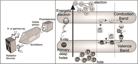
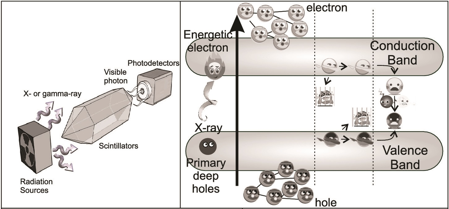
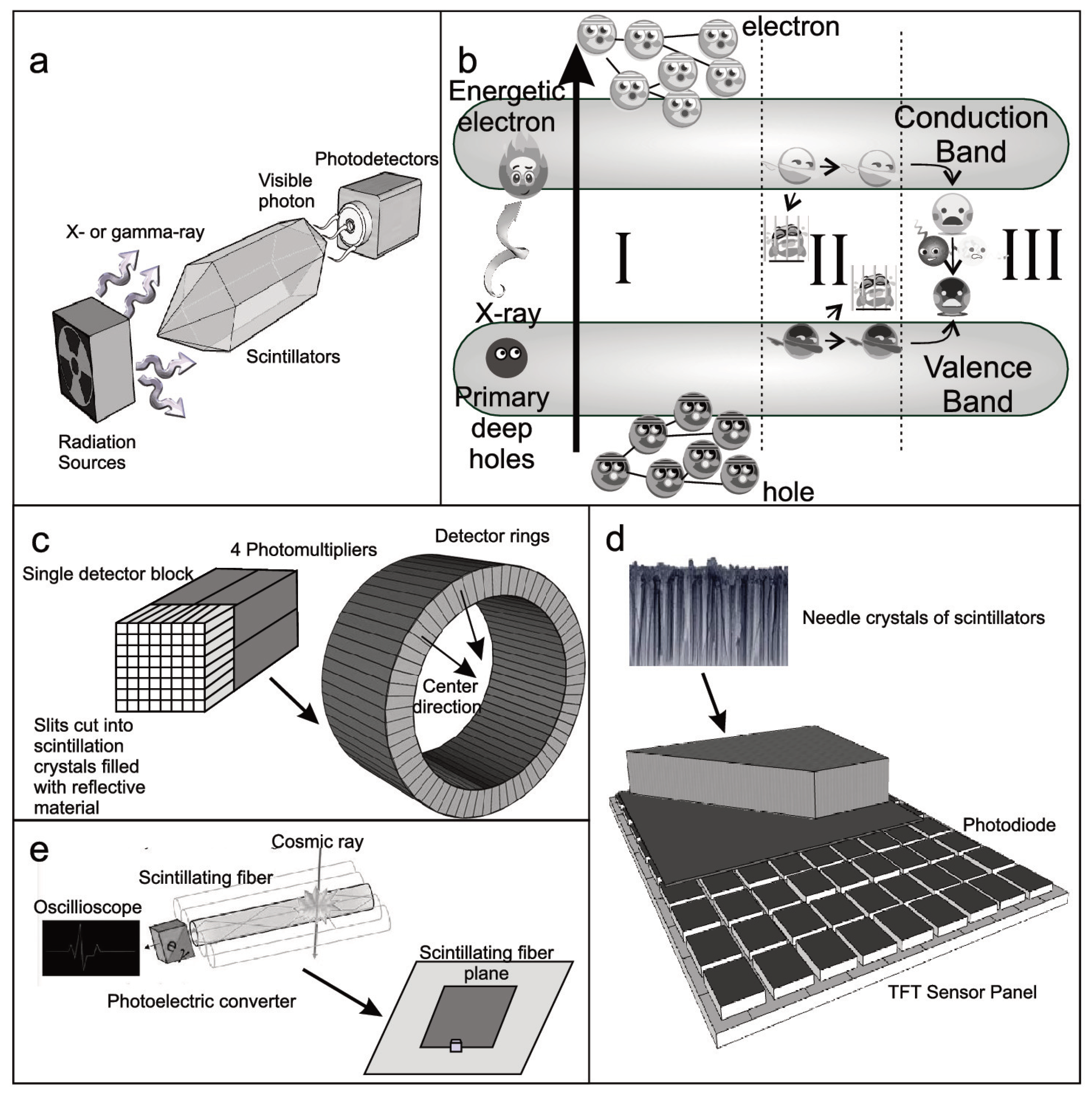
2. Concept of Scintillators and Applications
2.1. Mechanism of the Scintillation Process
2.2. Applications of Scintillators
2.3. Material Requirements for Scintillators
- Radiation absorption efficiency, absorption coefficient or absorption length: This parameter determines how efficiently a material will absorb the radiation during the conversion stage of scintillation. For X-ray and -ray detection, materials with high density and high atomic number are preferred as discussed in Section 2.1. A related concept, applied to particle radiation rather than photons, is stopping power, which is a measure of how efficiently a material can absorb the kinetic energy of a particle.
- Light yield (LY): the number of photons emitted per unit of deposited energy. This is one of the most important parameters of scintillators, playing a major role in determining the scintillators’ efficiency, sensitivity, and energy resolution. The light yield depends on by the number of electron–hole pairs that can be created in the ionization tracks resulting from the interaction of the incident photon and the scintillating material. The number of electron–hole pairs and thus, the light yield are related to the bandgap of the compound [26]. The light yield, expressed in photons/MeV, is given by the relation: , where S is the efficiency of electron–hole transport to the optical center, Q is the is the luminescence quantum efficiency of the optical center and is a constant, usually with a value of ∼2.5. Once the light is produced, some losses also occur during the transport to the detector, depending on internal scattering and re-absorption, hence, the actual light yield of a scintillator might be lower than the theoretically expected value, depending also on the geometry of the scintillator.
- Response time: the length of time for the scintillator to emit a UV/Vis photon after radiation absorption. The response time is mainly determined by the decay time of the scintillation. Fast response times, hence, short decay times, are very important for applications where timing is involved such as computer tomography or particle detection in accelerators. However, additional trapping process prior the luminescence in some scintillators, i.e., afterglow, is a disadvantage for this application. Some quenching processes may accelerate the decay as well, but at the cost of the light yield.
- Self-absorption of light: For the scintillator, the optical transmission for the nominal thickness for the scintillation spectrum should be considered. If there is too much self-absorption, the converted photons will be reabsorbed and can be lost through non-radiative processes.
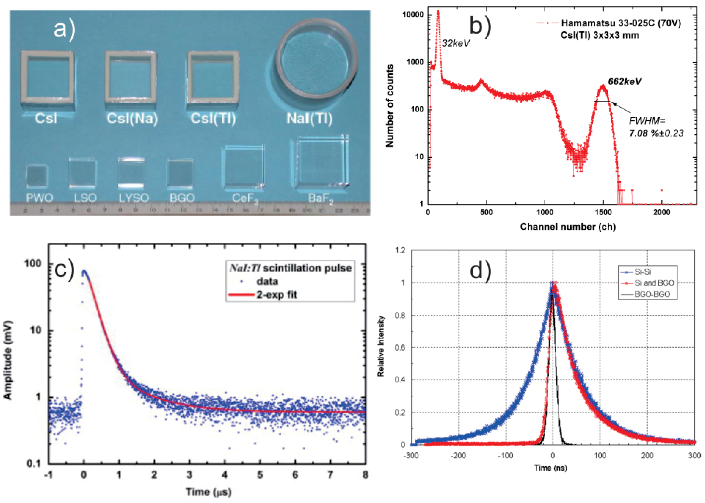
- Energy resolution: the ratio of the full width at half maximum (FWHM) of the peak at a certain energy in response to the exciting radiation, divided by the peak energy position in the pulse height spectrum. This feature is mainly important for spectral measurements of the incoming radiation, in particular for applications in -ray spectroscopy, and the ability of the scintillator to discriminated between different radiation energies. The intrinsic resolution of a scintillator is mainly determined by the non-proportional response of the material, but imperfections such as inhomogeneities in the scintillator resulting into local variations in light output and non-uniform reflectivity can also affect the energy resolution.
- Emission wavelength: A spectrum emitted by the scintillator after being excited by the radiation should match the spectrum of the photo-detector, in order to avoid post-scintillation losses. This is called spectral matching and is often more of an engineering rather than a material problem, requiring that the sensitivity and efficiency of the detector is near its peak in the spectral region where the scintillator emits. However, materials might need to be tailored in order to conform their emission to available commercial detectors.
- Stability: This is divided into chemical and radiation stability. Chemical stability pertains to the intrinsic stability of the material, including self-life. Radiation stability, also called radiation hardness, pertains the ability of the material not to degrade significantly when exposed to radiation. The stability determines thus, how long a material can be used as a scintillator before it needs to be changed.
- Proportionality: The scintillation response should be linear with the incident radiation, which can affect intensity discrimination. Although nowadays with computational method it is possible to correct a non-linear response with relative ease, it is still preferable in many occasions to have a linear response of the scintillator, at least in the energy range of interest.
- Spatial resolution: The parameter is usually known as a modulation transfer function (MTF). This is the spatial frequency response of an imaging system or a component. It is the contrast at a given spatial frequency relative to low frequencies and it is involved in the conversion of contrast values of different-sized objects (object contrast) into contrast intensity levels in the image (image contrast). The value is relevant to the effective resolution, which accounts for the amounts of blur and contrast over a range of spatial frequencies.
- Imaging performance: This is usually the detective quantum efficiency (DQE). Unlike MTF, it is the combined effects of the signal (related to image contrast) and noise performance of an imaging system, generally expressed as a function of spatial frequency. The effective of X-ray imaging for producing an image with high signal-to-noise ratio relative to an ideal detector.
3. Traditional Scintillators
3.1. Traditional Inorganic Scintillators
3.2. Traditional Organic Scintillators
4. Lanthanide Doped Scintillators
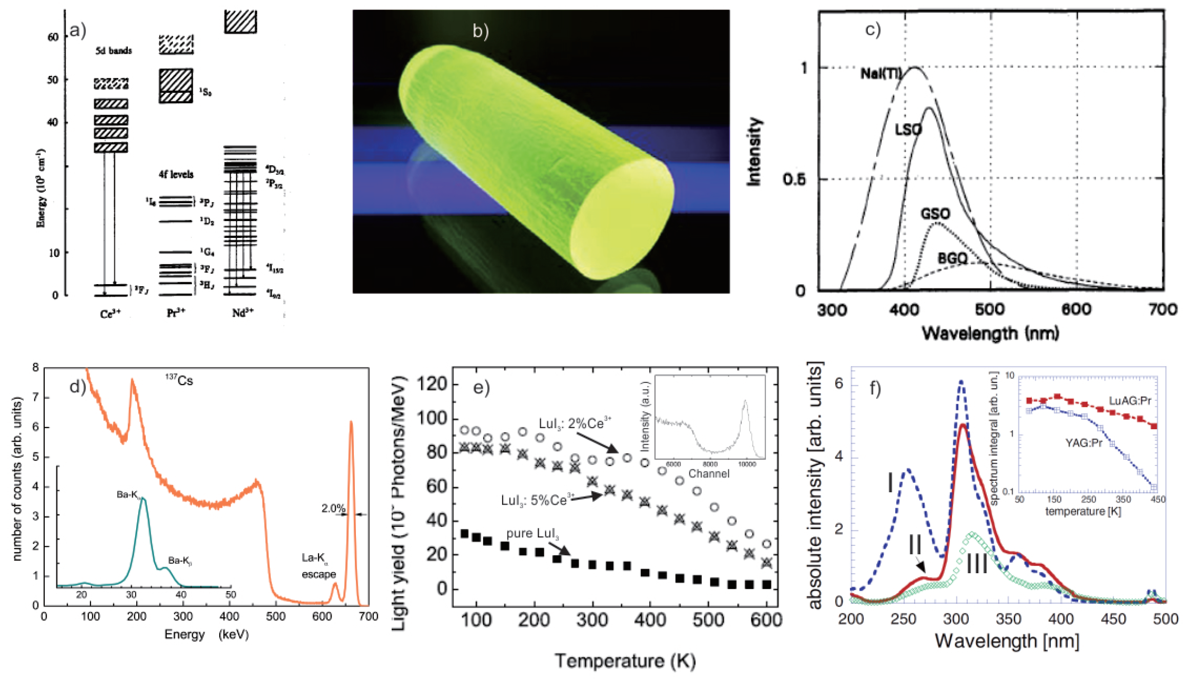
4.1. , , and Doped Scintillators
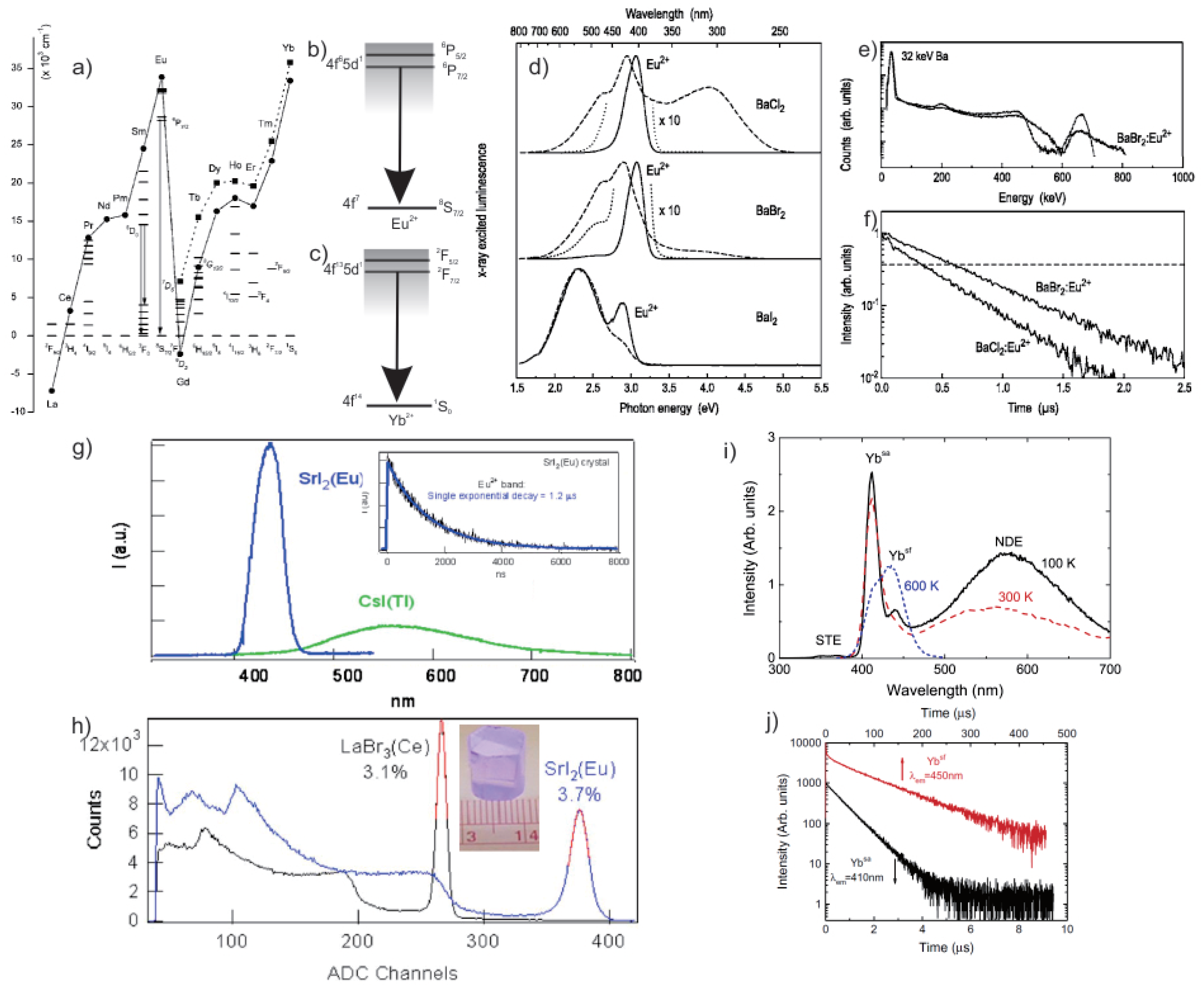
4.2. and Doped Scintillators
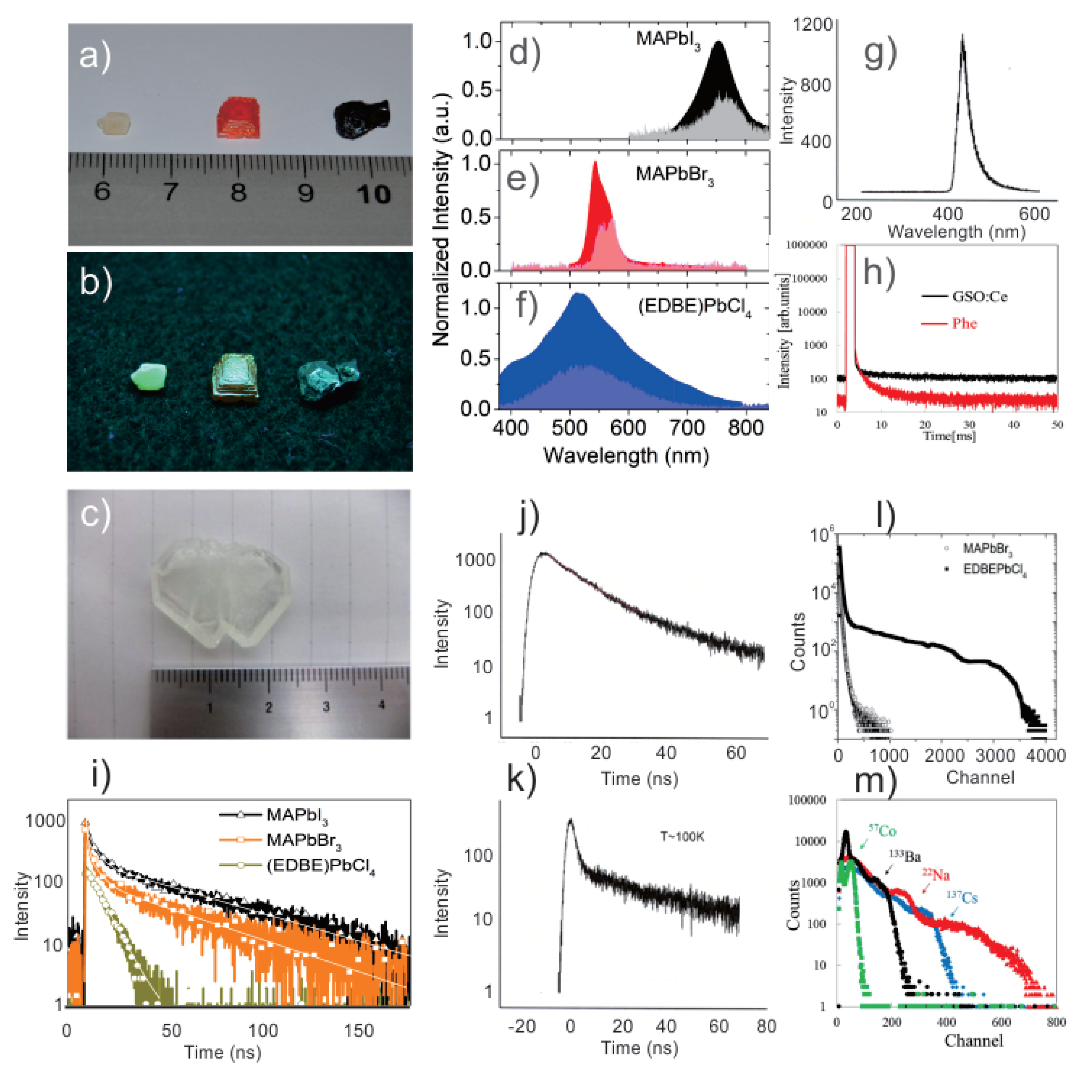
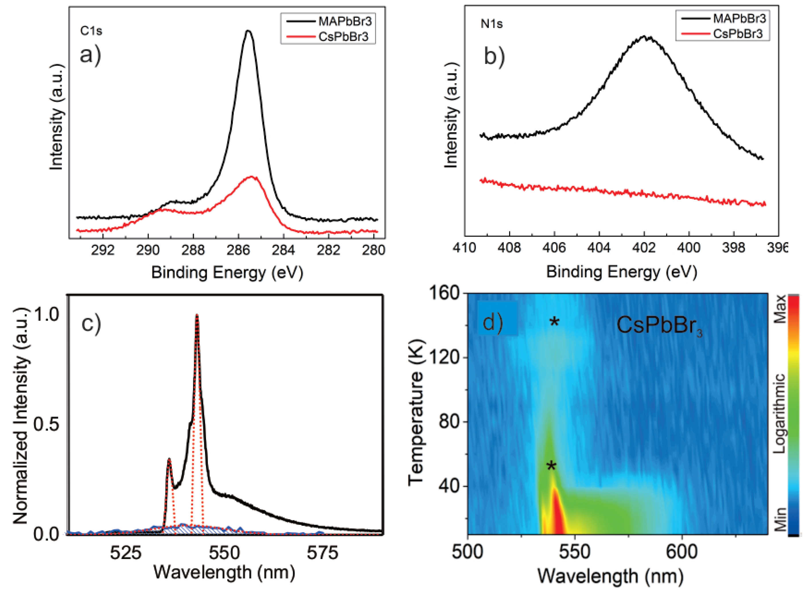
5. Perovskite Scintillators: Advantages and Limitations
6. Nanotechnology Improvements for Scintillators
6.1. Nanostructuring of Bulk Scintillators
6.1.1. Self-Assembled Methods
6.1.2. Lithographic Methods
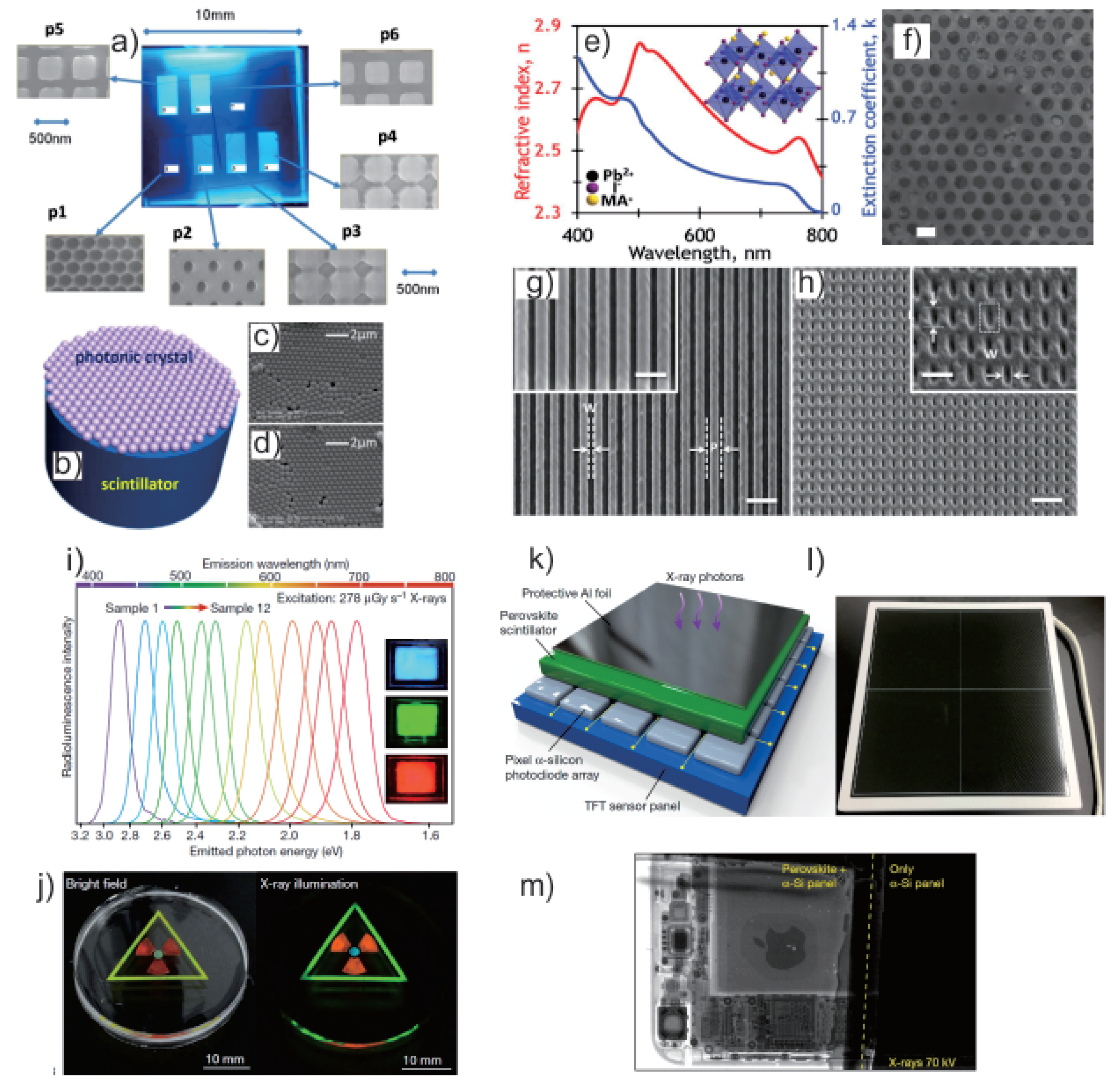
- Electron beam lithographyElectron beam lithography (EBL) is used to create patterns on a resist layer. Such method gives highly accurate pattern but due to its serial nature of the pattern writing, it is rather impracticable for mass production. The patterns are then transferred by etching techniques such as Reactive Ion Etching (RIE) to an intermediate layer such as silicon nitride (), if the scintillator material is not etchable by standard lithographic methods. Figure 7a shows photonic crystals of patterned by EBL on top of scintillator [156]. Light yield improvement of 20-60% compared to unpatterned scintillator is demonstrated [159]. Recently our co-workers Hou et al. demonstrated high enhancement of PL intensity from photonic crystal of perovskite thin film. The PMMA patterns are transferred directly to the perovskite material, without any intermediate layer, to form the perovskite photonic crystal [160]. This ability to pattern hygroscopic perovskite material, combined with excellent scintillation properties of perovskite material will be promising for future applications. Figure 7e,f shows the refractive index of and the SEM picture of perovskite photonic crystals, respectively.
- Soft X-ray interference lithographyUsing a mask consisting of four diffraction gratings creating interference patterns, conical holes of 45 nm thick of PMMA is patterned on . layer is then deposited using Atomic Layer Deposition (ALD). The high refractive index of the conformal layer enables light extraction enhancement of up to 95.1% [161]. This technique is mass scalable however the patterns are limited to those which can be produced from wave interference.
- Direct thermal nanoimprint lithographyUsing commercially available nanoimprinting stamp [162], low lasing threshold of 3.8 J/cm has been demonstrated from 2D photonic crystal on . This low threshold shows the good quality of the nanostructured perovskite which might be potential for scintillating applications. The nanoimprinting technique also gives the advantage of mass scalability.
6.1.3. Focused Ion Beam (FIB) Milling
6.2. QD and Nanocrystal Scintillators
6.2.1. II-VI QDs
6.2.2. Perovskite Nanocrystals
7. Summary
Author Contributions
Acknowledgments
Conflicts of Interest
References
- Rodnyi, P.A. Physical Processes in Inorganic Scintillators, 1st ed.; CRC Press: Boca Raton, FL, USA, 1997. [Google Scholar]
- Knoll, G. Radiation Detection and Measurement; Wiley: Hoboken, NJ, USA, 2000. [Google Scholar]
- Lecoq, P.; Gektin, A.; Korzhik, M. Inorganic Scintillators for Detector Systems, 2nd ed.; Springer International Publishing: Berlin, Germany, 2017. [Google Scholar]
- Russo, P. Handbook of X-ray Imaging: Physics and Technology; CRC Press: Boca Raton, FL, USA, 2018. [Google Scholar]
- Lille, S.; Marshall, W. Mammographic Imaging; Wolters Kluwer: South Holland, The Netherlands, 2018. [Google Scholar]
- Attix, F. Introduction to Radiological Physics and Radiation Dosimetry; Wiley: Hoboken, NJ, USA, 2004. [Google Scholar]
- Webb, W.R.; Major, N.M. Fundamentals of Body CT; Elsevier Health Sciences: Amsterdam, The Netherlands, 2014. [Google Scholar]
- Nikl, M. Scintillation detectors for X-rays. Meas. Sci. Technol. 2006, 17, R37. [Google Scholar] [CrossRef]
- Bailey, D.L.; Townsend, D.W.; Valk, P.; Maisey, M. Positron Emission Tomography; Springer: London, UK, 2005. [Google Scholar]
- Barkhausen, J.; Rody, A.; Schäfer, F.K.W. Digital Breast Tomosynthesis: Technique and Case; George Thieme Verlag KG: Stuttgart, Germany, 2016. [Google Scholar]
- Grajo, J.R.; Patino, M.; Prochowski, A.; Sahani, D.V. Dual energy CT in practice: Basic principles and applications. Appl. Rad. 2016, 45, 6–12. [Google Scholar]
- Anger, H.O. Scintillation Camera. Rev. Sci. Instrum. 1958, 29, 27–33. [Google Scholar] [CrossRef]
- MacAllister, D.; Miller, K.; Yang, C.; Graham, S. Application of X-ray CT scanning to determine gas/water relative permeabilities. SPE Form. Eval. 1993, 3, 184–188. [Google Scholar] [CrossRef]
- Dujardin, C.; Auffray, E.; Bourret-Courchesne, E.; Dorenbos, P.; Lecoq, P.; Nikl, M.; Vasilév, A.N.; Yoshikawa, A.; Zhu, R. Needs, Trends, and Advances in Inorganic Scintillators. IEEE Trans. Nucl. Sci. 2018, 65, 1977–1997. [Google Scholar] [CrossRef]
- Nikl, M.; Yoshikawa, A. Recent R&D Trends in Inorganic Single-Crystal Scintillator Materials for Radiation Detection. Adv. Opt. Mater. 2015, 3, 463–481. [Google Scholar]
- Blasse, G. Scintillator Materials. Chem. Mater. 1994, 6, 1465–1467. [Google Scholar] [CrossRef]
- Röntgen, W.C. On a New Kind of Rays. Science 1896, 3, 227–231. [Google Scholar] [CrossRef]
- Weber, M.J. Inorganic scintillators: Today and tomorrow. J. Lumin. 2002, 100, 35–45. [Google Scholar] [CrossRef]
- Brooks, F. Development of organic scintillators. Nucl. Instrum. Methods Phys. Res. 1979, 162, 477–505. [Google Scholar] [CrossRef]
- Lecoq, P. Development of new scintillators for medical applications. Nucl. Instrum. Methods Phys. Res. 2016, 809, 130–139. [Google Scholar] [CrossRef]
- van Eijk, C.W.E.; de Haas, J.T.M.; Rodnyi, P.A.; Khodyuk, I.V.; Shibuya, K.; Nishikido, F.; Koshimizu, M. Scintillation properties of a crystal of (C6H5(CH2)2NH3)2PbBr4. In Proceedings of the 2008 IEEE Nuclear Science Symposium Conference Record, Dresden, Germany, 19–25 October 2008; pp. 3525–3528. [Google Scholar]
- Birowosuto, M.D.; Cortecchia, D.; Drozdowski, W.; Brylew, K.; Lachmanski, W.; Bruno, A.; Soci, C. X-ray Scintillation in Lead Halide Perovskite Crystals. Sci. Rep. 2016, 6, 37254. [Google Scholar] [CrossRef] [PubMed]
- Nabet, B. Photodetectors, Materials, Devices and Applications; Woodhead Publishing: Sawston, UK, 2016. [Google Scholar]
- van Eijk, C.W.E. Fast scintillators and their applications. Radiat. Meas. 1993, 21, 5–10. [Google Scholar] [CrossRef]
- van Eijk, C.W.E.; Dorenbos, P.; Visser, R. Nd3+ and Pr3+ doped inorganic scintillators. IEEE Trans. Nucl. Sci. 1994, 41, 738–741. [Google Scholar] [CrossRef]
- Lempicki, A.; Wojtowicz, A.; Berman, E. Fundamental limits of scintillator performance. Nucl. Instrum. Methods Phys. Res. A 1993, 333, 304–311. [Google Scholar] [CrossRef]
- Rodnyi, P.A.; Dorenbos, P.; van Eijk, C.W.E. Energy Loss in Inorganic Scintillators. Phys. Stat. Sol. B 1995, 187, 15–29. [Google Scholar] [CrossRef]
- Dorenbos, P. Scintillation mechanisms in Ce3+ doped halide scintillators. Phys. Stat. Sol. A 2005, 202, 195–200. [Google Scholar] [CrossRef]
- Hall, H. The Theory of Photoelectric Absorption for X-rays and y-Rays. Rev. Mod. Phys. 1936, 29, 358–397. [Google Scholar] [CrossRef]
- Eisenberg, P.; Platzman, P. Compton Scattering of X Rays from Bound Electrons. Phys. Rev. A 1970, 2, 415–423. [Google Scholar] [CrossRef]
- Hubbell, J. Electron–positron pair production by photons: A historical overview. Rad. Phys. Chem. 2006, 75, 614–623. [Google Scholar] [CrossRef]
- Kinchin, G.H.; Pease, R.S. The Displacement of Atoms in Solids by Radiation. Rep. Prog. Phys. 1955, 18, 1. [Google Scholar] [CrossRef]
- Frenkel, J. Über die Wärmebewegung in festen und flüssigen Körpern. Z. Phys. 1926, 35, 652–669. [Google Scholar] [CrossRef]
- Karim, D.P.; Aldred, A.T. Localized level hopping transport in La(Sr)CrO3. Phys. Rev. B 1979, 20, 2255–2263. [Google Scholar] [CrossRef]
- Shepherd, J.A.; Gruner, S.M.; Tate, M.W.; Tecotzky, M. Study of afterglow in X-ray phosphors for use on fast-framing charge-coupled device detectors. Opt. Eng. 1997, 36, 36–36. [Google Scholar] [CrossRef]
- Blasse, G. New Luminescent Materials. Chem. Mater. 1989, 3, 294–301. [Google Scholar] [CrossRef]
- Kerisit, S.; Rosso, K.M.; Cannon, B.D.; Gao, F.; Xie, Y. Computer simulation of the light yield nonlinearity of inorganic scintillators. J. Appl. Phys. 2009, 105, 114915. [Google Scholar] [CrossRef]
- Dujardin, C.; Pedrini, C.; Blanc, W.; Gacon, J.C.; van’t Spijker, J.C.; Frijns, O.W.V.; van Eijk, C.W.E.; Dorenbos, P.; Chen, R.; Fremout, A.; et al. Optical and scintillation properties of large crystals. J. Phys. Condens. Matter 1998, 10, 3061–3073. [Google Scholar] [CrossRef]
- Wojtowicz, A.; Drozdowski, W.; Ptaszyk, M.; Galazka, Z.; Lefaucheur, J.L. Scintillation Light Yield of Ce-Doped LuAP and LuYAP Pixel Crystals. In Proceedings of the 8th International Conference on Inorganic Scintillators and Their Use in Scientific and Industrial Applications, Kharkov, Ukraine, 19–23 September 2005; Gektin, A.V., Ed.; National Academy of Sciences of Ukraine: Kiev, Ukraine, 2006; pp. 473–476. [Google Scholar]
- ter Weele, D.N.; Schaart, D.R.; Dorenbos, P. The Effect of Self-Absorption on the Scintillation Properties of Ce3+ Activated LaBr3 and CeBr3. IEEE Trans. Nucl. Sci. 2014, 61, 683–688. [Google Scholar] [CrossRef]
- Melcher, C.L. Scintillation Crystals for PET. J. Nucl. Med. 2000, 41, 1501–1505. [Google Scholar]
- Melcher, C.L.; Schweitzer, S. Cerium-doped lutetium oxyorthosilicate: A fast, efficient new scintillator. IEEE Trans. Nucl. Sci. 1992, 39, 502–505. [Google Scholar] [CrossRef]
- Tian, Y.; Cao, W.H.; Luo, X.X.; Fu, Y. Preparation and luminescence property of Gd2O2S:Tb X-ray nano-phosphors using the complex precipitation method. J. Alloy. Compd. 2007, 433, 313–317. [Google Scholar] [CrossRef]
- Leblans, P.; Struye, L.; Willems, P. A new needle-crystalline computed radiography detector. J. Digit. Imaging 2000, 13, 117–120. [Google Scholar] [CrossRef] [PubMed]
- Neitzel, U. Status and prospects of digital detector technology for CR and DR. Radiat. Prot. Dosim. 2005, 114, 32–38. [Google Scholar] [CrossRef]
- Sawant, A.; Antonuk, L.E.; El-Mohri, Y.; Zhao, Q.; Li, Y.; Su, Z.; Wang, Y.; Yamamoto, J.; Du, H.; Cunningham, I.; et al. Segmented crystalline scintillators: An initial investigation of high quantum efficiency detectors for megavoltage X-ray imaging. Med. Phys. 2005, 32, 3067–3083. [Google Scholar] [CrossRef] [PubMed]
- Schaefer-Prokop, C.; Neitzel, U.; Venema, H.W.; Uffmann, M.; Prokop, M. Digital chest radiography: an update on modern technology, dose containment and control of image quality. Eur. Radiol. 2008, 18, 1818–1830. [Google Scholar] [CrossRef]
- Pititeeraphab, Y.; Laksanapanai, B.; Lertprasert, P.; Pintaviroo, C. X-ray-Detector with CMOS Sensor Camera. In Proceedings of the World Congress of Medical Physics and Biomedical Engineering, Seoul, Korea, 27 August–1 Septmber 2006; Magjarevic, R., Nagel, J.H., Eds.; Springer: Berlin/Heidelberg, Germany, 2006; pp. 813–816. [Google Scholar]
- Rocha, J.; Minas, G.; Lanceros-Mendez, S. Optical coupling between scintillators and standard CMOS detectors. Nucl. Instrum. Methods Phys. Res. A 2006, 556, 281–286. [Google Scholar] [CrossRef]
- Takahashi, T.; Gunji, S.; Hirayama, M.; Kamae, T.; Miyazaki, S.; Sekimoto, Y.; Tamura, T.; Tanaka, M.; Yamasaki, N.Y.; Yamagami, T.; et al. Newly developed low background hard X-ray/gamma-ray telescope with the well-type phoswich counters. IEEE Trans. Nucl. Sci. 1993, 40, 890–898. [Google Scholar] [CrossRef]
- Biswas, S.; Das, S.; Ghosh, S.; Nag, D.; Raha, S. Development of scintillator detector for detection of cosmic ray shower. J. Instrum. 2017, 12, C06026. [Google Scholar] [CrossRef]
- Atac, M.; Streets, J.; Wilcer, N. Detection of cosmic ray tracks using scintillating fibers and position sensitive multi-anode photomultipliers. AIP Conf. Proc. 1998, 422, 251–256. [Google Scholar]
- Bross, A.D. Applications for Large Solid Scintillator Detectors in Neutrino and Particle Astrophysics. Nucl. Phys. B Proc. Suppl. 2000, 229–232, 363–367. [Google Scholar] [CrossRef]
- Annenkov, A.N.; Buzanov, O.; Danevich, F.; Georgadze, A.; Kim, S.; J. Kim, H.; D Kim, Y.; Kobychev, V.; Kornoukhov, V.; Korzhik, M.; et al. Development of CaMoO4 crystal scintillators for double beta decay experiment with 100-Mo. Nucl. Instrum. Methods Phys. Res. A 2008, 584, 334–345. [Google Scholar] [CrossRef]
- Crookes, W. Certain Properties of the Emanations of Radium. Chem. News 1903, 87, 241. [Google Scholar]
- Hofstadter, R. Alkali Halide Scintillation Counters. Phys. Rev. 1948, 74, 100–101. [Google Scholar] [CrossRef]
- Porter, F.; Freedman, M.; Wagner, F.; Sherman, I. Response of NaI, anthracene and plastic scintillators to electrons and the problems of detecting low energy electrons with scintillation counters. Nucl. Instrum. Methods Phys. Res. 1966, 39, 35–44. [Google Scholar] [CrossRef]
- Blahuta, S.; Bessiere, A.; Viana, B.; Dorenbos, P.; Ouspenski, V. Evidence and Consequences of Ce4+ in LYSO: Ce, Ca and LYSO: Ce, Mg Single Crystals for Medical Imaging Applications. IEEE Trans. Nucl. Sci. 2013, 60, 3134–3141. [Google Scholar] [CrossRef]
- Nikl, M.; Kamada, K.; Babin, V.; Pejchal, J.; Pilarova, K.; Mihokova, E.; Beitlerova, A.; Bartosiewicz, K.; Kurosawa, S.; Yoshikawa, A. Defect Engineering in Ce-Doped Aluminum Garnet Single Crystal Scintillators. Cryst. Growth Des. 2014, 14, 4827–4833. [Google Scholar] [CrossRef]
- Moretti, F.; Hovhannesyan, K.; Derdzyan, M.; Bizarri, G.A.; Bourret, E.D.; Petrosyan, A.G.; Dujardin, C. Consequences of Ca Codoping in YAlO3:Ce Single Crystals. Chem. Phys. Chem. 2017, 18, 493–499. [Google Scholar] [CrossRef]
- Moszynski, M.; Balcerzyk, M.; Czarnacki, W.; Nassalski, A.; Szczęśniak, T.; Kraus, H.; Mikhailik, V.; Solskii, I. Characterization of CaWO4 Scintillator at Room and Liquid Nitrogen Temperatures. Nucl. Instrum. Methods Phys. Res. A 2005, 553, 578–591. [Google Scholar] [CrossRef]
- Bauer, R.; Weingart, R. Fabrication of thin NaI(TI) scintillation layers for low energy X-ray detection. Nucl. Instrum. Methods Phys. Res. 1967, 55, 55–60. [Google Scholar] [CrossRef]
- Nagarkar, V.V.; Gupta, T.K.; Miller, S.R.; Klugerman, Y.; Squillante, M.R.; Entine, G. Structured CsI(Tl) scintillators for X-ray imaging applications. IEEE Trans. Nucl. Sci. 1998, 45, 492–496. [Google Scholar] [CrossRef]
- van Eijk, C.; Dorenbos, P.; van Loef, E.; Krämer, K.; Güdel, H. Energy resolution of some new inorganic-scintillator gamma-ray detectors. Rad. Meas. 2001, 33, 521–525. [Google Scholar] [CrossRef]
- Sakai, E. Recent Measurements on Scintillator-Photodetector Systems. IEEE Trans. Nucl. Sci. 1987, 34, 418–422. [Google Scholar] [CrossRef]
- Moszyński, M.; Allemand, R.; Laval, M.; Odru, R.; Vacher, J. Recent progress in fast timing with CsF scintillators in application to time-of-flight positron tomography in medicine. Nucl. Instrum. Methods Phys. Res. 1983, 205, 239–249. [Google Scholar] [CrossRef]
- Laval, M.; Moszyński, M.; Allemand, R.; Cormoreche, E.; Guinet, P.; Odru, R.; Vacher, J. Barium fluoride—Inorganic scintillator for subnanosecond timing. Nucl. Instrum. Methods Phys. Res. 1983, 206, 169–176. [Google Scholar] [CrossRef]
- Derenzo, S.E.; Moses, W.W.; Cahoon, J.L.; Perera, R.C.C.; Litton, J.E. Prospects for new inorganic scintillators. IEEE Trans. Nucl. Sci. 1990, 37, 203–208. [Google Scholar] [CrossRef]
- Kinloch, D.R.; Novak, W.; Raby, P.; Toepke, I. New developments in cadmium tungstate. IEEE Trans. Nucl. Sci. 1994, 41, 752–754. [Google Scholar] [CrossRef]
- Kapusta, M.; Pawelke, J.; Moszyński, M. Comparison of YAP and BGO for high-resolution PET detectors. Nucl. Instrum. Methods Phys. Res. A 1998, 404, 413–417. [Google Scholar] [CrossRef]
- Schotanus, P.; Dorenbos, P.; Ryzhikov, V.D. Detection of CdS(Te) and ZnSe(Te) scintillation light with silicon photodiodes. IEEE Trans. Nucl. Sci. 1992, 39, 546–550. [Google Scholar] [CrossRef]
- Raue, R.; Shiiki, M.; Matsukiyo, H.; Toyama, H.; Yamamoto, H. Saturation of ZnS:Ag and Al under cathode X-ray excitation. J. Appl. Phys. 1994, 75, 481–488. [Google Scholar] [CrossRef]
- Hotta, S. Electronic and Optical Properties of Conjugated Molecular Systems in Condensed Phases; Research Signpost: Kerala, India, 2003. [Google Scholar]
- Yanagida, T.; Watanabe, K.; Fujimoto, Y. Comparative study of neutron and gamma-ray pulse shape discrimination of anthracene, stilbene, and p-terphenyl. Nucl. Instrum. Methods Phys. Res. A 2015, 784, 111–114. [Google Scholar] [CrossRef]
- Bass, C.; Beise, E.; Breuer, H.; Heimbach, C.; Langford, T.; Nico, J. Characterization of a 6Li-loaded liquid organic scintillator for fast neutron spectrometry and thermal neutron detection. Appl. Radiat. Isot. 2013, 77, 130–138. [Google Scholar] [CrossRef] [PubMed]
- Birks, J.B. Scintillations from Organic Crystals: Specific Fluorescence and Relative Response to Different Radiations. Proc. Phys. Soc. Sect. A 1951, 64, 874. [Google Scholar] [CrossRef]
- Zaitseva, N.; Glenn, A.; Carman, L.; Martinez, H.P.; Hatarik, R.; Klapper, H.; Payne, S. Scintillation properties of solution-grown trans-stilbene single crystals. Nucl. Instrum. Methods Phys. Res. A 2015, 789, 8–15. [Google Scholar] [CrossRef]
- Smeltzer, J.C. Energy Dependence of the Naphthalene Scintillation Detector. Rev. Sci. Instrum. 1950, 21, 669–669. [Google Scholar] [CrossRef] [PubMed]
- Adrova, N.A.; Koton, M.M.; Florinsky, F.S. Preparation of 2,5-diphenyloxazole and its. scintillation efficiency in plastics. Bull. Acad. Sci. USSR 1957, 6, 394–395. [Google Scholar] [CrossRef]
- Wegh, R.T.; Donker, H.; Oskam, K.D.; Meijerink, A. Visible Quantum Cutting in LiGdF4:Eu3+ Through Downconversion. Science 1999, 283, 663–666. [Google Scholar] [CrossRef] [PubMed]
- Yu, D.; Martín-Rodríguez, R.; Zhang, Q.; Meijerink, A.; Rabouw, F.T. Multi-photon quantum cutting in Gd2O2S:Tm3+ to enhance the photo-response of solar cells. Light Sci. Appl. 2015, 4, e344. [Google Scholar] [CrossRef]
- Zych, E.; Meijerink, A.; de Mello Doneg, C. Quantum efficiency of europium emission from nanocrystalline powders of Lu2O3:Eu. J. Phys. Condens. Matter 2003, 15, 5145–5155. [Google Scholar] [CrossRef]
- Birowosuto, M.D.; Dorenbos, P. Novel γ- and X-ray Scintillator Research: On the Emission Wavelength, Light Yield and Time Response of Ce3+ Doped Halide Scintillators. Phys. Status Solidi A 2009, 206, 9–20. [Google Scholar] [CrossRef]
- Moszyński, M.; Wolski, D.; Ludziejewski, T.; Kapusta, M.; Lempicki, A.; Brecher, C.; Wiśniewski, D.; Wojtowicz, A. Properties of the new LuAP:Ce scintillator. Nucl. Instrum. Methods Phys. Res. A 1997, 385, 123–131. [Google Scholar] [CrossRef]
- Drozdowski, W.; Wojtowicz, A.J.; Lukasiewicz, T.; Kisielewski, J. Scintillation properties of LuAP and LuYAP crystals activated with Cerium and Molybdenum. Nucl. Instrum. Methods Phys. Res. A 2006, 562, 254–261. [Google Scholar] [CrossRef]
- Alekhin, M.S.; de Haas, J.T.M.; Khodyuk, I.V.; Kramer, K.W.; Menge, P.R.; Ouspenski, V.; Dorenbos, P. Improvement of γ-ray energy resolution of LaBr3:Ce3+ scintillation detectors by Sr2+ and Ca2+ co-doping. Appl. Phys. Lett. 2013, 102, 161915. [Google Scholar] [CrossRef]
- Bessiere, A.; Dorenbos, P.; van Eijk, C.; Krämer, K.; Güdel, H.; de Mello Donega, C.; Meijerink, A. Luminescence and scintillation properties of the small bandgap compound LaI3:Ce3+. Nucl. Instrum. Methods Phys. Res. A 2005, 537, 22–26. [Google Scholar] [CrossRef]
- Birowosuto, M.D.; Dorenbos, P.; de Haas, J.T.M.; van Eijk, C.W.E.; Krämer, K.W.; Güdel, H.U. Optical Spectroscopy and Luminescence Quenching of LuI3:Ce3+. J. Lumin. 2006, 118, 308–316. [Google Scholar] [CrossRef]
- Birowosuto, M.D.; Dorenbos, P.; van Eijk, C.W.E.; Krämer, K.W.; Güdel, H.U. High-light-output scintillator for photodiode readout: LuI3:Ce3+. J. Appl. Phys. 2006, 99, 123520. [Google Scholar] [CrossRef]
- Birowosuto, M.D.; Dorenbos, P.; van Eijk, C.W.E.; Krämer, K.W.; Güdel, H.U. Scintillation properties of LuI3:Ce3+-high–light yield scintillators. IEEE Trans. Nucl. Sci. 2005, 52, 1114–1118. [Google Scholar] [CrossRef]
- C Watson, C.; Casey, M.; Eriksson, L.; Mulnix, T.; Adams, D.; Bendriem, B. NEMA NU 2 performance tests for scanners with intrinsic radioactivity. J. Nucl. Med. 2004, 45, 822–6. [Google Scholar]
- Moses, W.; Derenzo, S. The scintillation properties of cerium-doped lanthanum fluoride. Nucl. Instrum. Methods Phys. Res. A 1990, 299, 51–56. [Google Scholar] [CrossRef]
- Schotanus, P.; Eijk, C.V.; Hollander, R. Detection of LaF3:Nd3+ scintillation light in a photosensitive multiwire chamber. Nucl. Instrum. Methods Phys. Res. A 1988, 272, 913–916. [Google Scholar] [CrossRef]
- Dorenbos, P.; Visser, R.; van Eijk, C.W.E.; Khaidukov, N.M.; Korzhik, M.V. Scintillation properties of some Ce3+ and Pr3+ doped inorganic crystals. IEEE Trans. Nucl. Sci. 1993, 40, 388–394. [Google Scholar] [CrossRef]
- van Loef, E.V.D.; Dorenbos, P.; van Eijk, C.W.E.; Krämer, K.; Güdel, H.U. High-energy-resolution scintillator:Ce3+ activated LaCl3. Appl. Phys. Lett. 2000, 77, 1467–1468. [Google Scholar] [CrossRef]
- Birowosuto, M.D.; Dorenbos, P.; van Eijk, C.W.E.; Krämer, K.W.; Güdel, H.U. Thermal Quenching of Ce3+ Emission in PrX3 (X = Cl, Br) by Intervalence Charge Transfer. J. Phys. Condens. Matter 2007, 19, 256209. [Google Scholar] [CrossRef]
- van Loef, E.V.D.; Dorenbos, L.P.; van Eijk, C.W.E.; Kramer, K.; Gudel, H.U. Scintillation properties of LaCl3:Ce3+ crystals: fast, efficient, and high-energy resolution scintillators. IEEE Trans. Nucl. Sci. 2001, 48, 341–345. [Google Scholar] [CrossRef]
- Glodo, J.; van Loef, E.; Hawrami, R.; Higgins, W.M.; Churilov, A.; Shirwadkar, U.; Shah, K.S. Selected Properties of Cs2LiYCl6, Cs2LiLaCl6, and Cs2LiLaBr6 Scintillators. IEEE Trans. Nucl. Sci. 2011, 58, 333–338. [Google Scholar] [CrossRef]
- Bessiere, A.; Dorenbos, P.; van Eijk, C.W.E.; Kramer, K.W.; Gudel, H.U. New thermal neutron scintillators: Cs2LiYCl6:Ce3+ and Cs2LiYBr6:Ce3+. IEEE Trans. Nucl. Sci. 2004, 51, 2970–2972. [Google Scholar] [CrossRef]
- van Loef, E.V.D.; Glodo, J.; Higgins, W.M.; Shah, K.S. Optical and scintillation properties of Cs2LiYCl6:Ce3+ and Cs2LiYCl6:Pr3+ crystals. IEEE Trans. Nucl. Sci. 2005, 52, 1819–1822. [Google Scholar] [CrossRef]
- van ’t Spijker, J.; Dorenbos, P.; van Eijk, C.; Krämer, K.; Güdel, H. Scintillation and luminescence properties of Ce3+ doped K2LaCl5. J. Lumin. 1999, 85, 1–10. [Google Scholar] [CrossRef]
- van’t Spijker, J.; Frijns, O.W.V.; Dorenbos, P.; van Eijk, C.; Krämer, K.; Güdel, H. RbGd2Cl7:Ce3+ and RbGd2Br7: Ce3+: New Scintillators with a High Light Yield. In Proceedings of the International Conference on Inorganic Scintillators and their Applications, Shanghai, China, 22–25 September 1997; Yin, Z., Ed.; Crystal Clear Collaboration, Chinese Academy of Sciences: Shanghai, China, 1997; Volume 2, p. 330. [Google Scholar]
- van Loef, E.V.D.; Dorenbos, P.; van Eijk, C.W.E.; Krämer, K.; Güdel, H.U. High-energy-resolution scintillator:Ce3+ activated LaBr3. Appl. Phys. Lett. 2001, 79, 1573–1575. [Google Scholar] [CrossRef]
- Glodo, J.; Farrell, R.; van Loef, E.V.D.; Higgins, W.M.; Shah, K.S. LaBr3:Pr3+—A new red-emitting scintillator. IEEE Nucl. Sci. Symp. Conf. Rec. 2005, 1, 98–101. [Google Scholar]
- van Loef, E.; Dorenbos, P.; van Eijk, C.; Krämer, K.; Güdel, H. Optical and scintillation properties of pure and Ce3+ doped GdBr3. Opt. Comm. 2001, 189, 297–304. [Google Scholar] [CrossRef]
- Birowosuto, M.D.; Dorenbos, P.; van Eijk, C.W.E.; Krämer, K.W.; Güdel, H.U. Scintillation and luminescence properties of Ce3+ doped ternary cesium rare-earth halides. Phys. Stat. Sol. A 2007, 204, 850–860. [Google Scholar] [CrossRef]
- Birowosuto, M.D.; Dorenbos, P.; van Eijk, C.W.E.; Krämer, K.W.; Güdel, H.U. Scintillation properties and anomalous Ce3+ emission of Cs2NaREBr6:Ce3+ (RE = La, Y, Lu). J. Phys. Condens. Matter 2006, 18, 6133–6148. [Google Scholar] [CrossRef] [PubMed]
- van Loef, E.; Dorenbos, P.; van Eijk, C.; Krämer, K.; Güdel, H. Scintillation properties of K2LaX5:Ce3+ (X = Cl, Br, I). Nucl. Instrum. Methods Phys. Res. A 2005, 537, 232–236. [Google Scholar] [CrossRef]
- Birowosuto, M.D.; Dorenbos, P.; Haas, J.T.M.D.; Eijk, C.W.E.V.; Krämer, K.W.; Güdel, H.U. Li-Based Thermal Neutron Scintillator Research; Rb2LiYBr6:Ce3+ and Other Elpasolites. IEEE Trans. Nucl. Sci. 2008, 55, 1152–1155. [Google Scholar] [CrossRef]
- Birowosuto, M.D.; Dorenbos, P.; Bizarri, G.; van Eijk, C.W.E.; Kraemer, K.W.; Guedel, H.U. Temperature dependent scintillation and luminescence characteristics of GdI3: Ce3+. IEEE Trans. Nucl. Sci. 2008, 55, 1164–1169. [Google Scholar] [CrossRef]
- Grabmeier, B.C.; Rossner, W.; Berthold, T. Phospors in X-ray Computed Tomography and for the gamma-ray Anger Camera. In Proceedings of the International Conference on Inorganic Scintillators and Their Applications, Delft, The Netherlands, 28 August–September 1 1995; van Eijk, C.W.E., Ed.; Crystal Clear Collaboration, Delft University of Technology: Delft, The Nertherlands, 1995; Volume 1, p. 29. [Google Scholar]
- Moszyński, M.; Kapusta, M.; Wolski, D.; Klamra, W.; Cederwall, B. Properties of the YAP: Ce scintillator. Nucl. Instrum. Methods Phys. Res. A 1998, 404, 157–165. [Google Scholar] [CrossRef]
- Mihóková, E.; Nikl, M.; Mareš, J.; Beitlerová, A.; Vedda, A.; Nejezchleb, K.; Blažek, K.; D’Ambrosio, C. Luminescence and scintillation properties of YAG:Ce single crystal and optical ceramics. J. Lumin. 2007, 126, 77–80. [Google Scholar] [CrossRef]
- Ogino, H.; Yoshikawa, A.; Nikl, M.; Krasnikov, A.; Kamada, K.; Fukuda, T. Growth and scintillation properties of Pr-doped Lu3Al5O12 crystals. J. Crys. Growth 2006, 287, 335–338. [Google Scholar] [CrossRef]
- Nikl, M.; Yoshikawa, A.; Vedda, A.; Fukuda, T. Development of novel scintillator crystals. J. Cryst. Growth 2006, 292, 416–421. [Google Scholar] [CrossRef]
- Pauwels, D.; Masson, N.L.; Viana, B.; Kahn-Harari, A.; van Loef, E.V.D.; Dorenbos, P.; van Eijk, C.W.E. A novel inorganic scintillator: Lu2Si2O7:Ce3+ (LPS). IEEE Trans. Nucl. Sci. 2000, 47, 1787–1790. [Google Scholar] [CrossRef]
- Drozdowski, W.; Brylew, K.; Wojtowicz, A.J.; Kisielewski, J.; Świrkowicz, M.; ukasiewicz, T.; de Haas, J.T.; Dorenbos, P. 33000 photons per MeV from mixed (Lu0.75Y0.25)3Al5O12:Pr scintillator crystals. Opt. Mater. Express 2014, 4, 1207–1212. [Google Scholar] [CrossRef]
- Mareš, J.A.; Jacquier, B.; Pédrini, C.; Boulon, G. Fluorescence decays and lifetimes of Nd3+, Ce3+ and Cr3+ in YAG. Czech. J. Phys. B 1988, 38, 802–816. [Google Scholar] [CrossRef]
- Drozdowski, W.; Dorenbos, P.; de Haas, J.T.M.; Drozdowska, R.; Owens, A.; Kamada, K.; Tsutsumi, K.; Usuki, Y.; Yanagida, T.; Yoshikawa, A. Scintillation Properties of Praseodymium Activated Lu3Al5O12 Single Crystals. IEEE Trans. Nucl. Sci. 2008, 55, 2420–2424. [Google Scholar] [CrossRef]
- Melcher, C.L.; Schweitzer, J.S.; Peterson, C.A.; Manente, R.A.; Suzuki, H. Crystal growth and scintillation properties of the rare earth orthosilicates. In Proceedings of the International Conference on Inorganic Scintillators and Their Applications, Delft, The Netherlands, 28 August–1 September 1996; van Eijk, C.W.E., Ed.; Crystal Clear Collaboration, Delft University of Technology: Delft, The Netherlands, 1995; Volume 1, p. 309. [Google Scholar]
- Kawamura, S.; Kaneko, J.H.; Higuchi, M.; Yamaguchi, T.; Haruna, J.; Yagi, Y.; Susa, K.; Fujita, F.; Homma, A.; Nishiyama, S.; et al. Floating Zone Growth and Scintillation Characteristics of Cerium-Doped Gadolinium Pyrosilicate Single Crystals. IEEE Trans. Nucl. Sci. 2007, 54, 1383–1386. [Google Scholar] [CrossRef]
- Shimizu, S.; Kurashige, K.; Usui, T.; Shimura, N.; Sumiya, K.; Senguttuvan, N.; Gunji, A.; Kamada, M.; Ishibashi, H. Scintillation properties of Lu0.4Gd1.6SiO5: Ce (LGSO) crystal. IEEE Trans. Nucl. Sci. 2006, 53, 14–17. [Google Scholar] [CrossRef]
- Selling, J.; Birowosuto, M.D.; Dorenbos, P.; Schweizer, S. Europium-doped barium halide scintillators for X-ray and gamma-ray detections. J. Appl. Phys. 2007, 101, 034901. [Google Scholar] [CrossRef]
- Cherepy, N.J.; Hull, G.; Niedermayr, T.R.; Drobshoff, A.; Payne, S.A.; Roy, U.N.; Cui, Y.; Bhattacharaya, A.; Harrison, M.; Guo, M.; et al. Barium iodide single-crystal scintillator detectors. Proc. SPIE 2007, 6706. [Google Scholar]
- Gundiah, G.; Bourret-Courchesne, E.; Bizarri, G.; Hanrahan, S.M.; Chaudhry, A.; Canning, A.; Moses, W.W.; Derenzo, S.E. Scintillation properties of Eu2+-activated barium fluoroiodide. IEEE Trans. Nucl. Sci. 2010, 57, 3. [Google Scholar] [CrossRef]
- Gundiah, G.; Yan, Z.; Bizarri, G.; Derenzo, S.E.; Bourret-Courchesne, E.D. Structure and scintillation of Eu2+-activated BaBrCl and solid solutions in the BaCl2–BaBr2 system. J. Lumin. 2013, 138, 143–149. [Google Scholar] [CrossRef]
- Bourret-Courchesne, E.; Bizarri, G.; Borade, R.; Gundiah, G.; Samulon, E.; Yan, Z.; Derenzo, S. Crystal growth and characterization of alkali-earth halide scintillators. J. Crys. Growth 2012, 352, 78–83. [Google Scholar] [CrossRef]
- Bizarri, G.; Bourret-Courchesne, E.D.; Yan, Z.; Derenzo, S.E. Scintillation and Optical Properties BaBrI:Eu2+ and CsBa2I5:Eu2+. IEEE Trans. Nucl. Sci. 2011, 58, 3403–3410. [Google Scholar] [CrossRef]
- Derenzo, S.; Bizarri, G.; Borade, R.; Bourret-Courchesne, E.; Boutchko, R.; Canning, A.; Chaudhry, A.; Eagleman, Y.; Gundiah, G.; Hanrahan, S.; et al. New scintillators discovered by high-throughput screening. Nucl. Instrum. Methods Phys. Res. A 2011, 652, 247–250. [Google Scholar] [CrossRef]
- Holl, I.; Lorenz, E.; Mageras, G. A measurement of the light yield of common inorganic scintillators. IEEE Trans. Nucl. Sci. 1988, 35, 105–109. [Google Scholar] [CrossRef]
- Grippa, A.; Rebrova, N.; Gorbacheva, T.; Pedash, V.; Kosinov, N.; Cherginets, V.; Tarasov, V.; Tarasenko, O.; Lopin, A. Scintillation properties of CaBr2 crystals doped with Eu2+ ions. Nucl. Instrum. Methods Phys. Res. A 2013, 729, 356–359. [Google Scholar] [CrossRef]
- Cherepy, N.J.; Payne, S.A.; Asztalos, S.J.; Hull, G.; Kuntz, J.D.; Niedermayr, T.; Pimputkar, S.; Roberts, J.J.; Sanner, R.D.; Tillotson, T.M.; et al. Scintillators With Potential to Supersede Lanthanum Bromide. IEEE Trans. Nucl. Sci. 2009, 56, 873–880. [Google Scholar] [CrossRef]
- Borade, R.; Bourret-Courchesne, E.; Derenzo, S. Scintillation properties of CsBa2Br5:Eu2+. Nucl. Instrum. Methods Phys. Res. A 2011, 652, 260–263. [Google Scholar] [CrossRef]
- Rowe, E.; Bhattacharya, P.; Tupitsyn, E.; Groza, M.; Burger, A.; Cherepy, N.J.; Payne, S.A.; Sturm, B.W.; Pédrini, C. A New Lanthanide Activator for Iodide Based Scintillators:Yb2+. IEEE Trans. Nucl. Sci. 2013, 60, 1057–1060. [Google Scholar] [CrossRef]
- Zhuravleva, M.; Blalock, B.; Yang, K.; Koschan, M.; Melcher, C.L. New single crystal scintillators: CsCaCl3:Eu and CsCaI3:Eu. J. Cryst. Growth 2012, 352, 115–119. [Google Scholar] [CrossRef]
- Grippa, A.; Rebrova, N.; Gorbacheva, T.; Pedash, V.; Kosinov, N.; Cherginets, V.; Tarasov, V.; Tarasenko, O.; Lopin, A. Crystal growth and scintillation properties of CsCaBr3:Eu2+. J. Cryst. Growth 2013, 371, 112–116. [Google Scholar] [CrossRef]
- Cherginets, V.; Rebrova, N.; Grippa, A.; Datsko, Y.; Ponomarenko, T.; Pedash, V.; Kosinov, N.; Tarasov, V.; Zelenskaya, O.; Zenya, I.; et al. Scintillation properties of CsSrX3:Eu2+ (X = Cl, Br) single crystals grown by the Bridgman method. Mater. Chem. Phys. 2014, 143, 1296–1299. [Google Scholar] [CrossRef]
- Yang, K.; Zhuravleva, M.; Melcher, C.L. Crystal growth and characterization of CsSrI3:Eu2+ high–light yield scintillators. Phys. Stat. Sol. 2011, 5, 43–45. [Google Scholar]
- Stand, L.; Zhuravleva, M.; Chakoumakos, B.; Johnson, J.; Lindsey, A.; Melcher, C. Scintillation properties of Eu2+-doped KBa2I5 and K2BaI4. J. Lumin. 2016, 169, 301–307. [Google Scholar] [CrossRef]
- Cherepy, N.J.; Hull, G.; Drobshoff, A.D.; Payne, S.A.; Van Loef, E.; Wilson, C.M.; Shah, K.S.; Roy, U.N.; Burger, A.; Boatner, L.A.; et al. Strontium and barium iodide high–light yield scintillators. Appl. Phys. Lett. 2008, 92, 90–93. [Google Scholar] [CrossRef]
- Xie, A.; Nguyen, T.H.; Hettiarachchi, C.; Witkowski, M.E.; Drozdowski, W.; Birowosuto, M.D.; Wang, H.; Dang, C. Thermal Quenching and Dose Studies of X-ray Luminescence in Single Crystals of Halide Perovskites. J. Phys. Chem. C 2018, 122, 16265–16273. [Google Scholar] [CrossRef]
- Wei, H.; Fang, Y.; Mulligan, P.; Chuirazzi, W.; Fang, H.H.; Wang, C.; Ecker, B.R.; Gao, Y.; Loi, M.A.; Cao, L.; et al. Sensitive X-ray Detectors Made of Methylammonium Lead Tribromide Perovskite Single Crystals. Nat. Photon. 2016, 10, 333–339. [Google Scholar] [CrossRef]
- Kim, Y.C.; Kim, K.H.; Son, D.Y.; Jeong, D.N.; Seo, J.Y.; Choi, Y.S.; Han, I.T.; Lee, S.Y.; Park, N.G. Printable organometallic perovskite enables large-area, low-dose X-ray imaging. Nature 2017, 550, 87. [Google Scholar] [CrossRef] [PubMed]
- Wei, W.; Zhang, Y.; Xu, Q.; Wei, H.; Fang, Y.; Wang, Q.; Deng, Y.; Li, T.; Gruverman, A.; Cao, L.; et al. Monolithic integration of hybrid perovskite single crystals with heterogenous substrate for highly sensitive X-ray imaging. Nat. Photon. 2017, 11, 315. [Google Scholar] [CrossRef]
- Yakunin, S.; Sytnyk, M.; Kriegner, D.; Shrestha, S.; Richter, M.; Matt, G.J.; Azimi, H.; Brabec, C.J.; Stangl, J.; Kovalenko, M.V.; et al. Detection of X-ray photons by solution-processed lead halide perovskites. Nat. Photon. 2015, 9, 444–450. [Google Scholar] [CrossRef]
- Shrestha, S.; Fischer, R.; Matt, G.J.; Feldner, P.; Michel, T.; Osvet, A.; Levchuk, I.; Merle, B.; Golkar, S.; Chen, H.; et al. High-Performance Direct Conversion X-ray Detectors Based on Sintered Hybrid Lead Triiodide Perovskite Wafers. Nat. Photon. 2017, 11, 436–440. [Google Scholar] [CrossRef]
- Wei, H.; DeSantis, D.; Wei, W.; Deng, Y.; Guo, D.; Savenije, T.J.; Cao, L.; Huang, J. Dopant compensation in alloyed CH3NH3PbBr3-xClx perovskite single crystals for gamma-ray spectroscopy. Nat. Mater. 2017, 16, 826. [Google Scholar] [CrossRef]
- Tan, Z.K.; Moghaddam, R.S.; Lai, M.L.; Docampo, P.; Higler, R.; Deschler, F.; Price, M.; Sadhanala, A.; Pazos, L.M.; Credgington, D.; et al. Bright light-emitting diodes based on organometal halide perovskite. Nat. Nanotechnol. 2014, 9, 687–692. [Google Scholar] [CrossRef] [PubMed]
- Chin, X.Y.; Perumal, A.; Bruno, A.; Yantara, N.; Veldhuis, S.A.; Martínez-Sarti, L.; Chandran, B.; Chirvony, V.; Lo, A.S.Z.; So, J.; et al. Self-assembled hierarchical nanostructured perovskites enable highly efficient LEDs via an energy cascade. Energy Environ. Sci. 2018, 11, 1770–1778. [Google Scholar] [CrossRef]
- Shibuya, K.; Koshimizu, M.; Takeoka, Y.; Asai, K. Scintillation Properties of (C6H13NH3)2PbI4: Exciton Luminescence of an Organic/Inorganic Multiple Quantum Well Structure Compound Induced by 2.0 MeV protons. Nucl. Instrum. Methods Phys. Res. B 2002, 194, 207–212. [Google Scholar] [CrossRef]
- Kishimoto, S.; Shibuya, K.; Nishikido, F.; Koshimizu, M.; Haruki, R.; Yoda, Y. Subnanosecond time-resolved X-ray measurements using an organic-inorganic perovskite scintillator. Appl. Phys. Lett. 2008, 93, 261901. [Google Scholar] [CrossRef]
- Ma, D.; Fu, Y.; Dang, L.; Zhai, J.; Guzei, I.A.; Jin, S. Single-crystal microplates of two-dimensional organic–inorganic lead halide layered perovskites for optoelectronics. Nano Res. 2017, 10, 2117–2129. [Google Scholar] [CrossRef]
- Kawano, N.; Koshimizu, M.; Okada, G.; Fujimoto, Y.; Kawaguchi, N.; Yanagida, T.; Asai, K. Scintillating Organic-Inorganic Layered Perovskite-Type Compounds and the Gamma-Ray Detection Capabilities. Sci. Rep. 2017, 7, 14754. [Google Scholar] [CrossRef] [PubMed]
- Eperon, G.E.; Paternò, G.M.; Sutton, R.J.; Zampetti, A.; Haghighirad, A.A.; Cacialli, F.; Snaith, H.J. Inorganic caesium lead iodide perovskite solar cells. J. Mater. Chem. A 2015, 3, 19688–19695. [Google Scholar] [CrossRef]
- Diguna, L.J.; Tjahjana, L.; Darma, Y.; Zeng, S.; Wang, H.; Birowosuto, M.D. Light and Matter Interaction of Single Quantum Emitters with Dielectric Nanostructures. Photonics 2018, 5, 14. [Google Scholar] [CrossRef]
- Knapitsch, A.; Lecoq, P. Review on photonic crystal coatings for scintillators. Int. J. Mod. Phys. A 2014, 29, 1430070. [Google Scholar] [CrossRef]
- Salomoni, M.; Pots, R.; Auffray, E.; Lecoq, P. Enhancing Light Extraction of Inorganic Scintillators Using Photonic Crystals. Crystals 2018, 8, 78. [Google Scholar] [CrossRef]
- Liu, J.; Liu, B.; Zhu, Z.; Chen, L.; Hu, J.; Xu, M.; Cheng, C.; Ouyang, X.; Zhang, Z.; Ruan, J.; et al. Modified timing characteristic of a scintillation detection system with photonic crystal structures. Opt. Lett. 2017, 42, 987–990. [Google Scholar] [CrossRef] [PubMed]
- Knapitsch, A.; Auffray, E.; Fabjan, C.W.; Leclercq, J.; Letartre, X.; Mazurczyk, R.; Lecoq, P. Results of Photonic Crystal Enhanced Light Extraction on Heavy Inorganic Scintillators. IEEE Trans. Nucl. Sci. 2012, 59, 2334–2339. [Google Scholar] [CrossRef]
- Hou, S.; Xie, A.; Xie, Z.; Tobing, L.Y.M.; Zhou, J.; Tjahjana, L.; Yu, J.; Hettiarachichi, C.; Zhang, D.; Dang, C.; et al. Concurrent Inhibition and Redistribution of Spontaneous Emission from All Inorganic Perovskite Photonic Crystals. 2018. in submission. [Google Scholar]
- Zhu, Z.; Wu, S.; Xue, C.; Zhao, J.; Wang, L.; Wu, Y.; Liu, B.; Cheng, C. Enhanced light extraction of scintillator using large-area photonic crystal structures fabricated by soft-X-ray interference lithography. Appl. Phys. Lett. 2015, 106, 241901. [Google Scholar] [CrossRef]
- Pourdavoud, N.; Wang, S.; Mayer, A.; Hu, T.; Chen, Y.; Marianovich, A.; Kowalsky, W.; Heiderhoff, R.; Scheer, H.C.; Riedl, T. Photonic Nanostructures Patterned by Thermal Nanoimprint Directly into Organo-Metal Halide Perovskites. Adv. Mater. 2017, 29, 1605003. [Google Scholar] [CrossRef]
- Gholipour, B.; Adamo, G.; Cortecchia, D.; Krishnamoorthy, H.N.S.; Birowosuto, M.D.; Zheludev, N.I.; Soci, C. Organometallic Perovskite Metasurfaces. Adv. Mater. 2017, 29, 1604268. [Google Scholar] [CrossRef]
- Bulin, A.L.; Vasil’ev, A.; Belsky, A.; Amans, D.; Ledoux, G.; Dujardin, C. Modelling energy deposition in nanoscintillators to predict the efficiency of the X-ray-induced photodynamic effect. Nanoscale 2015, 7, 5744–5751. [Google Scholar] [CrossRef] [PubMed]
- Yaffe, M.J.; Rowlands, J.A. X-ray detectors for digital radiography. Phys. Med. Biol. 1997, 42, 1–39. [Google Scholar] [CrossRef]
- Kang, Z.; Zhang, Y.; Menkara, H.; Wagner, B.K.; Summers, C.J.; Lawrence, W.; Nagarkar, V. CdTe quantum dots and polymer nanocomposites for X-ray scintillation and imaging. Appl. Phys. Lett. 2011, 98, 181914. [Google Scholar] [CrossRef] [PubMed]
- Xu, G.; Zeng, S.; Zhang, B.; Swihart, M.T.; Yong, K.T.; Prasad, P.N. New Generation Cadmium-Free Quantum Dots for Biophotonics and Nanomedicine. Chem. Rev. 2016, 116, 12234–12327. [Google Scholar] [CrossRef] [PubMed]
- Burke, E.R.; DeHaven, S.L.; Williams, P.A. Scintillating quantum dots for imaging X-rays (SQDIX) for aircraft inspection. AIP Conf. Proc. 2016, 1706, 110007. [Google Scholar]
- Protesescu, L.; Yakunin, S.; Bodnarchuk, M.I.; Krieg, F.; Caputo, R.; Hendon, C.H.; Yang, R.X.; Walsh, A.; Kovalenko, M.V. Nanocrystals of Cesium Lead Halide Perovskites (CsPbX3, X = Cl, Br, and I): Novel Optoelectronic Materials Showing Bright Emission with Wide Color Gamut. Nano Lett. 2015, 15, 3692–3696. [Google Scholar] [CrossRef] [PubMed]
- Chen, Q.; Wu, J.; Ou, X.; Huang, B.; Almutlaq, J.; Zhumekenov, A.A.; Guan, X.; Han, S.; Liang, L.; Yi, Z.; et al. All-inorganic perovskite nanocrystal scintillators. Nature 2018, 561, 88–93. [Google Scholar] [CrossRef] [PubMed]
- Heo, J.H.; Shin, D.H.; Park, J.K.; Kim, D.H.; Lee, S.J.; Im, S.H. High-Performance Next-Generation Perovskite Nanocrystal Scintillator for Nondestructive X-ray Imaging. Adv. Mater. 2018, 30, 1801743. [Google Scholar] [CrossRef] [PubMed]


| Scintillator | (g/cm) | Light Yield (photons/MeV) | Energy Resolution (%, at 662keV) | (nm) | (ns) | Refs. | |
|---|---|---|---|---|---|---|---|
| : | 3.7 | 50.8 | 43,000 | 6.7 | 415 | 230 | [64,65] |
| : | 4.5 | 54.0 | 66,000 | 6.6 | 560 | 1000 | [64,65] |
| : | 4.5 | 54.0 | 43,000 | 7.4 | 425 | - | [65] |
| 4.6 | 53.2 | 1900 | 19 | 390 | 2–4 | [66] | |
| 4.9 | 52.7 | 1430 | 10 | 175 | 0.8 | [67] | |
| 6.1 | 75.6 | 15,800 | 6.3 | 425 | 6800 | [61] | |
| 8.3 | 75.6 | 140 | - | ∼475 | ∼10 | [68] | |
| 7.9 | 64.2 | 19,700 | 6.5 | 495 | 104 | [69] | |
| 7.1 | 75.2 | 8200 | 27 | 505 | 300 | [70] | |
| : | 4.8 | 48.0 | 17,000 | 14 | 640 | 270–3000 | [71] |
| : | 4.1 | 27.4 | 73,000 | - | 450 | 105 | [72] |
| Scintillator | Type | (g/cm) | Light Yield (photons/MeV) | (nm) | (ns) | Refs. | |
|---|---|---|---|---|---|---|---|
| Organic crystal | 1.25 | 5.24 | 16,000 | 447 | 30 | [57,74] | |
| Organic crystal | 1.16 | 5.14 | 8000 | 410 | 4.5 | [74,77] | |
| Organic crystal | 0.96 | 5.18 | 2000 | 348 | 80 | [78] | |
| 2,5- | Organic crystal | 1.06 | 5.52 | 8800 | 405 | 7 | [79] |
| p- | Liquid Solution | - | - | ∼9200 | 440 | 5 | [74] |
| Scintillator | (g/cm) | Light Yield (photons/MeV) | Energy Resolution (%, at 662 keV) | (nm) | (ns) | Ref. | |
|---|---|---|---|---|---|---|---|
| : | 5.9 | 40.3 | 2200 | - | 290 | 3 and 27 | [92] |
| : | 5.9 | 40.3 | 2000 | - | 173 | 6 | [93] |
| 6.2 | 41.1 | 4500 | - | 330 | 28 | [92] | |
| : | 8.3 | 50.2 | 8000 | - | 310 | 28 | [83] |
| : | 3.1 | 23.9 | 6900 | - | 240 | 20 | [94] |
| : | 3.9 | 49.5 | 49,000 | 3.3 | 330 | 25 | [95] |
| : | 4.0 | 51.5 | 21,000 | 8.4 | 340 | 17 | [96] |
| 3.9 | 50.4 | 28,000 | - | 360 | 25 | [97] | |
| : | 3.3 | 41.4 | 35,000 | 3.4 | 400 | 1 and 40 | [98] |
| : | 3.3 | 38.1 | 21,000 | 6.0 | 376 | 1 and 35 | [99] |
| : | 3.3 | 38.1 | 10,000 | 15.0 | 315 | 1 and 35 | [100] |
| : | 2.9 | 44.1 | 30,000 | 5.1 | 344 | 1000 | [101] |
| : | 3.7 | 53.9 | 40,000 | 5.0 | 370 | 90 | [102] |
| : | 5.1 | 46.9 | 67,000 | 2.8 | 358 | 15 | [103] |
| : | 5.1 | 46.9 | 75,000 | 3.2 | 450 to 900 | 11,000 | [104] |
| : | 5.3 | 48.3 | 21,000 | 5.5 | 365 | 6 | [96] |
| : | 4.6 | 52.4 | 44,000 | - | 350 | 20 | [105] |
| : | 4.6 | 42.7 | 10,400 | 30.0 | 390 | 46 | [106] |
| : | 3.9 | 46.9 | 17,000 | 11.3 | 414 | 61 | [107] |
| : | 3.9 | 44.5 | 9500 | 6.3 | 420 | 61 | [107] |
| : | 4.3 | 52.3 | 5800 | 10.5 | 422 | 61 | [107] |
| : | 3.3 | 44.1 | 60,000 | 2.9 | 410 | 55 | [98] |
| : | 4.1 | 41.5 | 24,000 | 7.0 | 389 | 85 | [99] |
| : | 3.9 | 42.8 | 40,000 | 4.9 | 359 | 100 | [108] |
| : | 3.9 | 42.1 | 33,000 | 4.8 | 363 | 26 | [109] |
| : | 3.8 | 35.9 | 23,000 | 4.7 | 385 | 42 | [109] |
| : | 4.8 | 50.6 | 56,000 | 3.8 | 420 | 43 | [102] |
| : | 4.4 | 52.4 | 57,000 | 4.2 | 401 | 24 | [108] |
| : | 5.2 | 56.9 | 47,000 | 4.7 | 525 | 45 | [110] |
| : | 4.7 | 57.0 | 2600 | - | 571 | - | [106] |
| : | 5.7 | 60.5 | 98,000 | 4.6 | 475 | 33 | [89] |
| : | 4.8 | 57.0 | 1500 | - | 429 | - | [106] |
| : | 4.8 | 57.9 | 22,800 | 9.0 | 556 | 18 | [106] |
| : | 7.3 | 61.1 | 40,000 | - | 511 | 3000 | [111] |
| : | 5.4 | 25.6 | 17,000 | 5.7 | 370 | 26 | [112] |
| : | 4.6 | 35.1 | 17,000 | 3.5 | 550 | 85 | [113] |
| : | 4.6 | 35.1 | 16,000 | - | 300 to 400 | 18 | [114] |
| : | 8.3 | 64.9 | 11,400 | 23 | 365 | 17 | [84] |
| : | 7.4 | 50.2 | 30,000 | 10 | 420 | 40 | [42] |
| : | 7.4 | 50.2 | 2200 | - | 247 | 26 | [115] |
| : | 6.2 | 46.4 | 26,000 | 9.5 | 378 | 38 | [116] |
| : | 6.2 | 44.1 | 33,000 | 4.4 | - | - | [117] |
| : | 6.7 | 44.3 | 12,500 | - | 510 | 70 | [118] |
| : | 6.7 | 44.3 | 19,000 | 4.6 | 310 | 20 | [119] |
| : | 6.7 | 45.3 | 12,500 | 7.0 | 430 | 56 | [120] |
| : | 5.5 | 41.8 | 40,000 | 6.0 | 372 | 46 | [121] |
| : | 7.3 | ∼63 | 30,000 to 39,000 | ∼8 | 410 to 430 | 30 to 40 | [122] |
| Scintillator | (g/cm) | Light Yield (photons/MeV) | Energy Resolution (%, at 662 keV) | (nm) | (ns) | Ref. | |
|---|---|---|---|---|---|---|---|
| : | 3.89 | 49.8 | 19,400 | 8.8 | 402 | 390 | [123] |
| : | 4.78 | 47.8 | 15,700 | 11.0 | 404 | 585 | [123] |
| : | 5.15 | 54.1 | 59,000 | 8.0 | 425 | 610 | [124] |
| : | 5.45 | 49.3 | 55,000 | 8.5 | 405 | 584 | [125] |
| : | 4.50 | 44.2 | 52,000 | 3.6 | 407 | 484 | [126] |
| : | 4.60 | 49.4 | 54,000 | 9.0 | 410 | - | [127] |
| : | 5.20 | 50.3 | 97,000 | 3.4 | 412 | 432 | [128] |
| : | 5.47 | 40.9 | 40,000 | - | 505 | 582 | [129] |
| : | 4.14 | 34.6 | 35,000 | - | 425 | 540 | [129] |
| : | 3.97 | 35.1 | 35,000 | - | 505 | 1296 | [129] |
| : | 3.73 | 33.4 | 30,000 | - | 520 | 2800 | [129] |
| : | 5.25 | 38.8 | 27,000 | - | 420 | 459 | [129] |
| : | 4.10 | 34.9 | 25,000 | - | 440 | 669 | [129] |
| : | 3.93 | 34.7 | 20,000 | - | 453 | 742 | [129] |
| : | 4.27 | 34.5 | 20,000 | - | 450 | 566 | [129] |
| : | 4.17 | 35.4 | 18,000 | - | 418 | 698 | [129] |
| : | 4.75 | 36.2 | 16,000 | - | 505 | 748 | [129] |
| : | 3.77 | 24.4 | 16,000 | - | 459 | 1100 | [129] |
| : | 3.75 | 32.8 | 11,000 | - | 420 | 640 | [129] |
| : | 4.26 | 35.8 | 10,000 | - | 505 | 692 | [129] |
| : | 3.40 | 15.5 | 24,000 | - | 430 | 940 | [130] |
| : | 3.35 | 35.3 | 36,000 | 9.1 | 448 | 2500 | [131] |
| : | 3.96 | 48.0 | 110,000 | 8.0 | 470 | 790 | [132] |
| : | 3.75 | 44.9 | 30,000 | - | 431 | - | [127] |
| : | 4.40 | 47.0 | 25,000 | - | 441 | - | [127] |
| : | 4.50 | 54.0 | 17,000 | - | 462 | - | [127] |
| : | 4.48 | 46.2 | 92,000 | - | 430 | 844 | [133] |
| : | 4.90 | 54.0 | 102,000 | 2.6 | 435 | 1200 | [128] |
| : | 4.90 | 54.0 | 54,000 | 5.7 | 414 | 870 | [134] |
| : | 3.00 | 44.3 | 18,000 | 8.9 | 445 | 5050 | [135] |
| : | 3.72 | 46.6 | 28,000 | 9.3 | 447 | 6097 | [136] |
| : | 4.06 | 54.0 | 38,500 | 8.0 | 450 | 1720 | [135] |
| : | 2.57 | 38.9 | 33,400 | 11.5 | 442 | 2700 | [137] |
| : | 3.34 | 42.1 | 31,300 | 9.0 | 448 | 2500 | [137] |
| : | 3.74 | 51.4 | 65,000 | 5.9 | 450 | 3300 | [138] |
| : | 4.12 | 49.4 | 63,000 | 2.9 | 448 | 1500 | [139] |
| : | 4.47 | 52.2 | 90,000 | 2.4 | 444 | 1700 | [139] |
| : | 4.22 | 36.1 | 20,000 | 7.0 | 410 | - | [132] |
| : | 4.60 | 49.4 | 85,000 | 3.7 | 422 | 1200 | [140] |
| : | 4.60 | 49.4 | 56,000 | 4.4 | 414 | 610 | [134] |
| : | 4.10 | 42.8 | 70,000 | - | 414 | - | [127] |
| : | 4.90 | 44.2 | 47,000 | - | 418 | - | [127] |
© 2019 by the authors. Licensee MDPI, Basel, Switzerland. This article is an open access article distributed under the terms and conditions of the Creative Commons Attribution (CC BY) license (http://creativecommons.org/licenses/by/4.0/).
Share and Cite
Maddalena, F.; Tjahjana, L.; Xie, A.; Arramel; Zeng, S.; Wang, H.; Coquet, P.; Drozdowski, W.; Dujardin, C.; Dang, C.; et al. Inorganic, Organic, and Perovskite Halides with Nanotechnology for High–Light Yield X- and γ-ray Scintillators. Crystals 2019, 9, 88. https://0-doi-org.brum.beds.ac.uk/10.3390/cryst9020088
Maddalena F, Tjahjana L, Xie A, Arramel, Zeng S, Wang H, Coquet P, Drozdowski W, Dujardin C, Dang C, et al. Inorganic, Organic, and Perovskite Halides with Nanotechnology for High–Light Yield X- and γ-ray Scintillators. Crystals. 2019; 9(2):88. https://0-doi-org.brum.beds.ac.uk/10.3390/cryst9020088
Chicago/Turabian StyleMaddalena, Francesco, Liliana Tjahjana, Aozhen Xie, Arramel, Shuwen Zeng, Hong Wang, Philippe Coquet, Winicjusz Drozdowski, Christophe Dujardin, Cuong Dang, and et al. 2019. "Inorganic, Organic, and Perovskite Halides with Nanotechnology for High–Light Yield X- and γ-ray Scintillators" Crystals 9, no. 2: 88. https://0-doi-org.brum.beds.ac.uk/10.3390/cryst9020088