1. Introduction
Solar cells have drawn much research interest in recent decades due to their important role in renewable energy production [
1,
2,
3]. Today, silicon is the predominant material used in the semiconductor devices of solar cells; however, solar cells based on III-V semiconductors exhibit superior energy conversion efficiencies. Many factors may affect the performance of solar cell devices. For example, the built-in electric field is the driving force of photogenerated carrier flow through external loads such as light bulbs or batteries. It has been reported that a high built-in electric field in the depletion region is helpful for photocarrier extraction from quantum wells [
4,
5]. Furthermore, it has been observed that a critical built-in electric field is necessary for an optimum carrier collection in multi-quantum well p-i-n diodes and a key factor in determining the open-circuit voltage (V
oc) [
6]. However, most characterization methods for solar cells, such as current–voltage (I-V) characteristics [
7], capacitance-voltage (C-V) characteristics [
8], and scanning Kelvin probe microscopy (SKPM) or scanning capacitance microscopy (SCM) [
9], can only measure the average or local built-in potential. Modulation spectroscopy, which employs various modulation techniques, such as photomodulation, electromodulation, piezomodulation and thermomodulation [
10,
11,
12,
13], is a powerful tool for studying fine structures in optical spectra of semiconductor devices and materials. Electroreflectance (ER) measurements are one kind of modulation spectroscopy which apply an AC voltage to a device under test to modulate the electric potential and thus the distribution of an electric field. ER spectra exhibit Franz–Keldysh oscillations (FKOs), from the oscillation period of which the electric field within the device can be determined experimentally. Therefore, the structural design and characteristic analysis of solar cell devices can benefit greatly from ER technology.
Another important consideration in the pursuit of the optimum device performance of solar cells is the collection of photogenerated carriers, which are pushed to the front and back surfaces of the cells. Usually, the back contact is simply a solid metal sheet and the front electrode is a mesh with many metal grids connected to bus bars. If we want to collect the photogenerated carriers more efficiently, more metal grids should be added to shorten the distance between the metal grids and to lower the spreading sheet resistance. However, incident light will be blocked by the metal grids and the effective cell area that is exposed to the sunlight for generating photocarriers will be reduced. Thus, an optimized grid pattern on the front contact is necessary for solar cells to perform well. Light beam induced current (LBIC) mapping uses a laser beam of small diameter to cause local excitation in a sample, through which electron-hole pairs are generated to give rise to a photocurrent and scan over the sample surface. LBIC mapping is a convenient tool for analyzation of the carrier collection efficiency at different positions on the surface and to find the low efficiency areas. Various groups have used the LBIC technique to investigate grain boundary distribution and to explain the minority carrier diffusion length and surface recombination velocity at a grain boundary or surface [
14,
15].
In this study, we measure ER modulation spectroscopy to estimate the electric field within the device. LBIC mapping is performed to evaluate the efficiency and sheet resistance of solar cells with different metal grid gaps. We also measure the photovoltaic characteristics of these solar cells by using an AM 1.5 solar simulator. The measurement results and extracted characteristic parameters are presented and discussed.
2. Materials and Methods
The p-i-n GaAs solar cell wafer was grown using metalorganic chemical vapor deposition (MOCVD). First an n-GaAs buffer layer (1 μm) was grown on the n-GaAs substrate, followed by an n-GaInP back surface field (BSF) layer (0.2 μm) and then a p-i-n structure consisting of an n-GaAs base (3 μm), an i-GaAs layer (0.02 μm) and a p-GaAs emitter layer (0.5 μm). Above the p-i-n structure, a p-GaInP window layer (0.05 μm) and a p-GaAs contact layer (0.3 μm) were grown. The detailed epitaxy growth information is listed in
Table 1. Several square samples with dimensions of about 3.4 × 3.4 mm
2 were prepared from the epitaxy wafer, and then underwent device processing. A metal sheet and metal grids were deposited by electron beam evaporation on the back side and front side of each sample, respectively, for ohmic contacts. The width of the metal grid was 20 μm. The intervals between metal grids for samples A, B, C and D were 600, 450, 300 and 150 μm, respectively.
The ER measurement uses an AC voltage signal with an amplitude of 0.1 V and a frequency of 200 Hz as the modulating source. The incident monochromatic light comes from a 150 W tungsten-halogen lamp filtered by a 0.25 m monochromator. The reflected light from the sample surface is detected by a Si photodetector, which outputs an electric signal composed of a DC level and an AC signal with the same frequency of the modulation voltage. A neutral density filter (ND filter) is equipped to maintain the DC level at a constant value and the AC signal is recorded by a lock-in amplifier.
The LBIC system uses a solid-state-diode-pumped (SSDP) laser (532 nm) focused with a 20× objective as the excitation source to induce the local photocurrent, which is then recorded by a picoammeter (Keithley 6485, Keithley Instruments, Solon, OH, USA), operating in the short-circuit mode. The diameter of the laser spot is about 14 μm. The samples are mounted on an x-y stage with a resolution of 1 μm, and the mapping procedures are controlled by a personal computer.
3. Results and Discussion
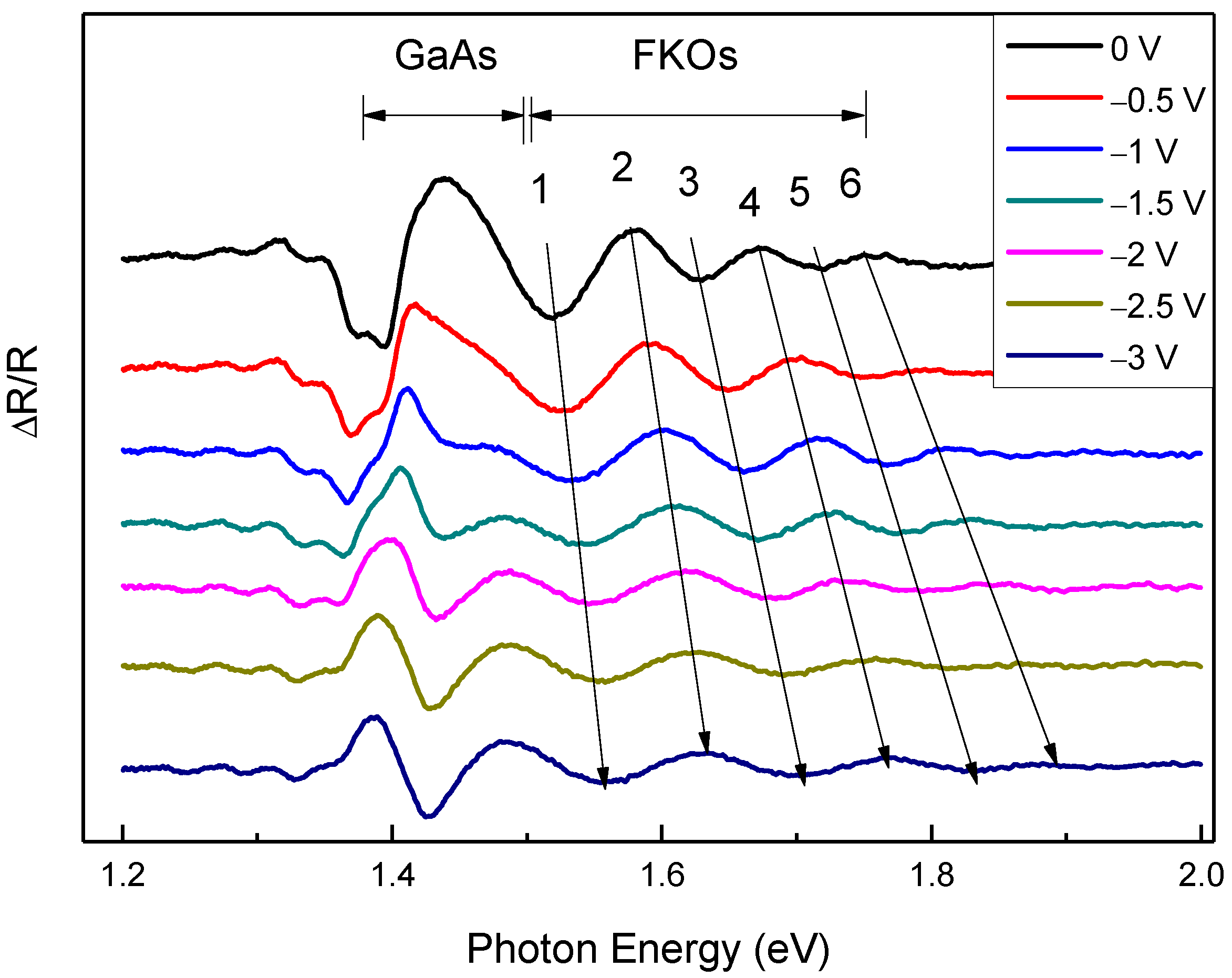
Figure 1 shows the ER spectra of sample A reversely biased at various voltages at 300 K. Samples B, C and D have similar ER spectra because all samples are from the same epitaxial wafer. For the purpose of easy observation and comparison, the ER spectra taken at different reverse biases have been shifted vertically. From the upper to the lower spectra, the bias voltage changes from 0 to −3 V with a step of −0.5 V. The bandgap transition feature starting at 1.42 eV has been observed in each spectrum, and several periods of FKOs follow behind the bandgap transition feature. The bandgap transition feature and FKOs in the ER spectra are characteristics of the Franz–Keldysh effect for a semiconductor in the presence of intermediate electric fields [
16]. Under an electric field, the wavefunctions of electrons in the conduction band and holes in the valence band are in the form of Airy functions with the exponential tail extending into the semiconductor bandgap. The overlap between electron and hole wavefunctions gives the optical absorption curve which shows a tail and oscillations below and above the bandgap energy, respectively. This phenomenon, in ER measurement, is manifested as the bandgap transition feature and FKOs shown in
Figure 1. As indicated by the arrows labeled 1–6, the extrema shift toward higher energy with increasing reverse bias is due to the increase of the built-in electric field. Based on the Franz–Keldysh theory, the electric field strength can be estimated by analyzing the period of FKOs [
17,
18,
19]. The ER line shape is expressed by [
19]
where
E is photon energy,
Γ a damping parameter,
ћΩ the electro-optic energy of carriers, and
θ a phase factor. The electro-optic energy
ћΩ is given by
where
e is the electronic charge,
ħ the reduced Planck constant,
F the built-in electric field and
μ the interband reduced effective mass in the field direction. The cosine term in Equation (1) has extrema at energies
Ej determined through the equation:
where
j is the index number of the
jth extremum.
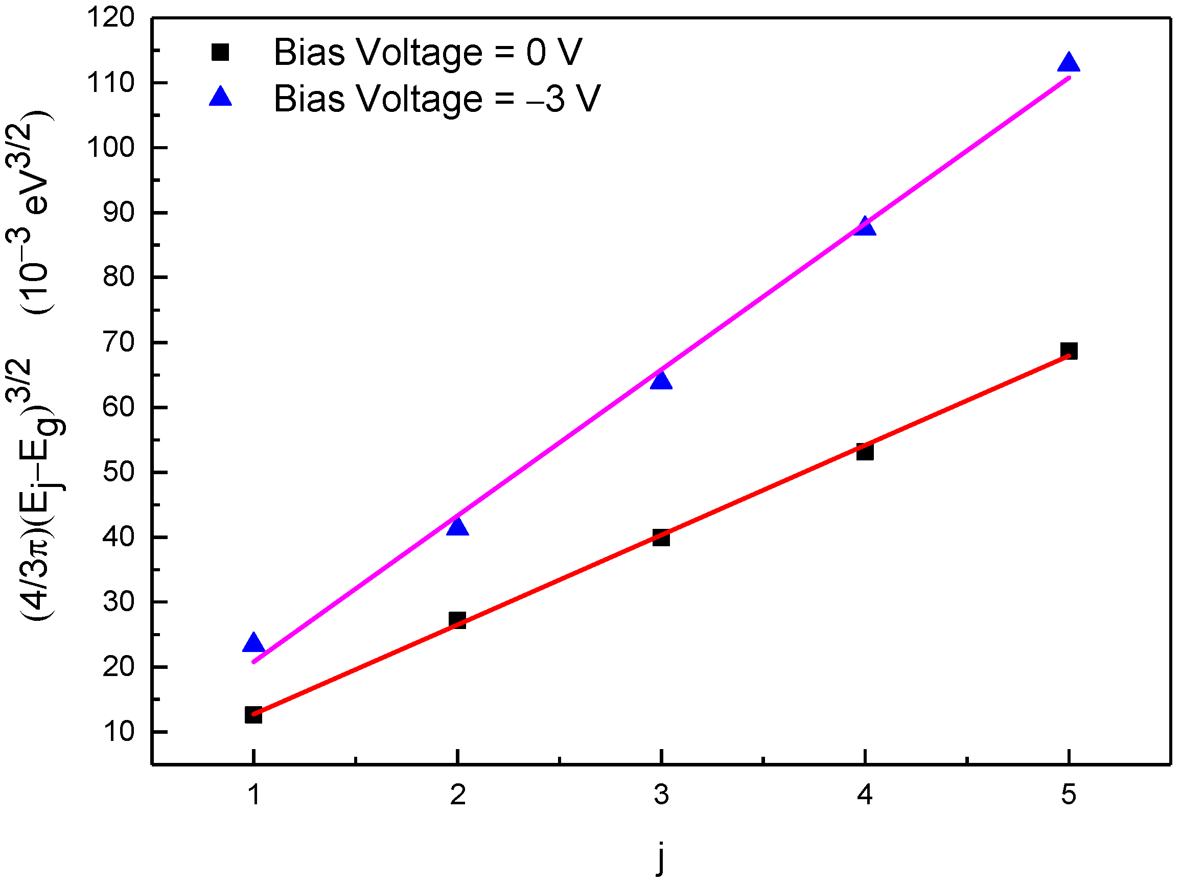
Figure 2 shows the quantity (4/3π)(
Ej −
Eg)
3/2 as a function of the index
j. The results are indicated by two straight lines connecting squares for zero bias and triangles for reverse bias of −3 V. From the slope of the straight line, the built-in electric field is determined to be 167 kV/cm at zero bias and 275 kV/cm at −3 V, respectively. This built-in electric field across the i-layer of a p-i-n structure is mainly determined by the doping levels in the n/p layers and the thickness of the i-layer. The doping levels are 2 × 10
18 cm
−3 and 3 × 10
17 cm
−3 respectively for the emitter and base layers of the p-i-n structure in this study. We have used capacitance-voltage (C-V) measurement to check the doping concentration of the lightly doped base layer and found the value is 2.65 × 10
17 cm
−3.
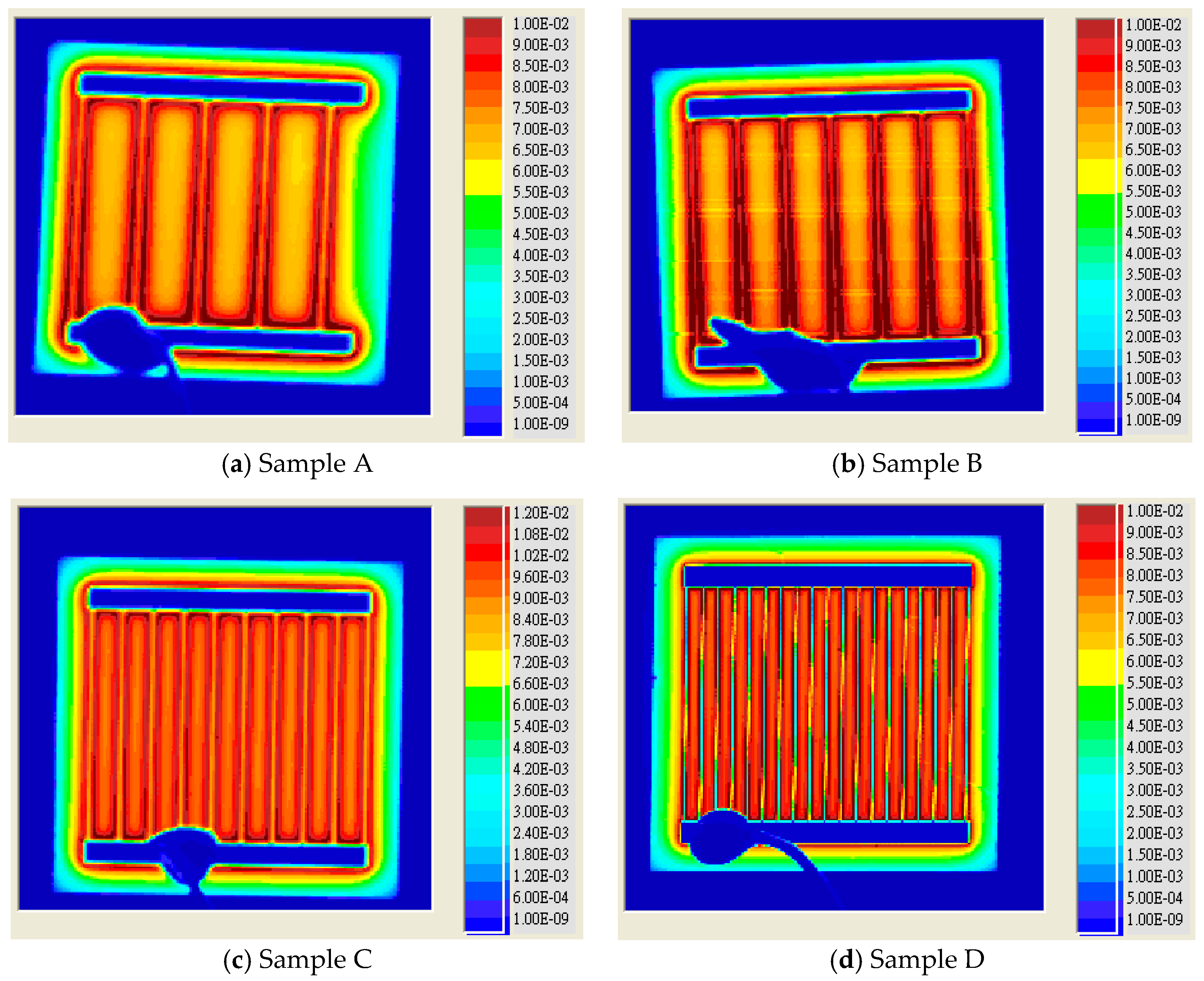
Figure 3 shows the LBIC mapping images of samples A to D. The scale bar is in an absolute scale with units of amperes (A). For each image, the blue background represents the area outside the sample area, and the two blue strips show the main bus bars, which block the transmission of the laser beam. Between the two bus bars, the metal grids, which are spaced 600 to 150 μm apart for samples A to D, respectively, have been clearly resolved.
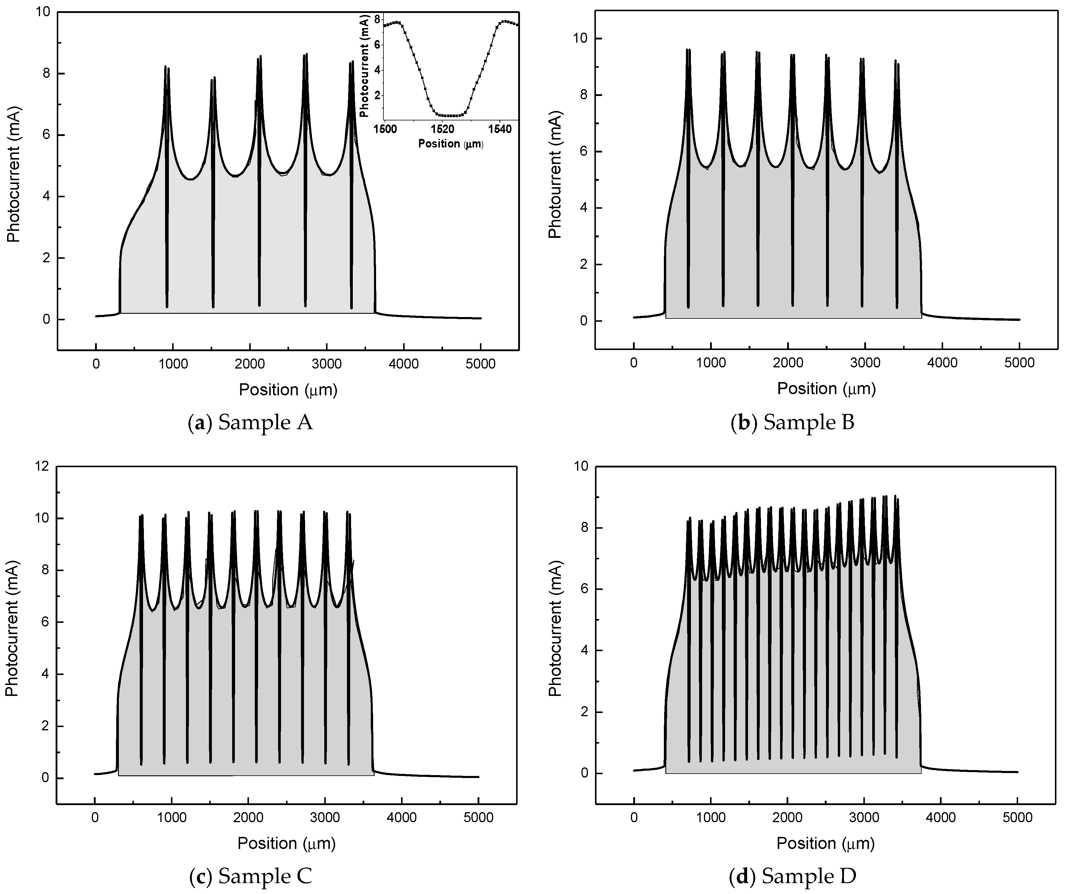
Figure 4 shows the LBIC signal trace crossing the metal grids for various samples. Taking sample A as the example, the LBIC profile located at the two sections within 0~305 μm and 3631~5000 μm shows almost no current response, because the laser beam is focused out of the sample. In
Figure 4a, there are five sharp dips located at 922, 1523, 2124, 2722 and 3321 μm, respectively, with a period of ~600 μm, which is exactly that of the original grid pattern design for sample A. The insertion in
Figure 4a illustrates the detailed profile around the dip and gives us information about the diameter of the laser beam spot. When the laser beam is focused on a metal grid (20 μm wide), the induced current will be very low, because the incident light is blocked by the metal grid. It can be seen that the lowest point of the dip spans about 6 μm, indicating a diameter of about 14 μm for the laser beam spot. For the other three samples B to D, as shown in
Figure 4b–d, the periods of the LBIC profile dips match well with the originally designed intervals between metal grids. These results confirm that the mapping system has good spatial resolution.
For all LBIC profiles shown in
Figure 4, the induced photocurrent starts increasing rapidly at around 300 μm, because the laser beam has been moved on to the solar cell. As the laser beam moves toward the grid, the current increases constantly. For example, in
Figure 4a, the induced photocurrent is 2.878 mA at the position of 400 μm, and increases to 3.821 mA at the position of 600 μm. At the peak position where the laser beam is focused adjacent to the grid edge, the induced photocurrent reaches a maximum. Thus, for each dip, two peaks show up on each side of the dip, which correspond to the two edges of a grid. As the laser beam sweeps from one metal grid to another, the photocurrent undergoes a maximum-minimum-maximum signal trace (with the sharp dips excluded). The maximum response happens when the laser spot hits the area adjacent to a grid edge, whereas the minimum response occurs at the midway position between two metal grids. Although a larger space between grids provides more area for light absorption, the increasing distance from the middle positions to the grids makes it difficult for the induced photo-carriers to reach the metal grids in order to contribute to the photocurrent. Integrating the LBIC profiles and taking sample A as a reference, the ratio of integrated photocurrent intensities for samples A to D is 1:1.17:1.33:1.16. The result shows that sample C performs best in terms of converting light to electric current, while sample A is the worst due to the overly wide spacing between the grids.
Furthermore, from the ratio of the maximum and minimum in a LBIC profile, the sheet resistance of the top region for carrier diffusion can be extracted using the equations [
20,
21]:
where
d is the distance between two metal grids,
ΩS is the sheet resistance and
σP is the shunt conductance. Using sample A for calculation, with the shunt conductance
σP of 0.583 S/cm
2 extracted from the I-V characteristics of the illuminated solar cell (to be presented later), the sheet resistance
ΩS is determined to be 2767
Ω/□.
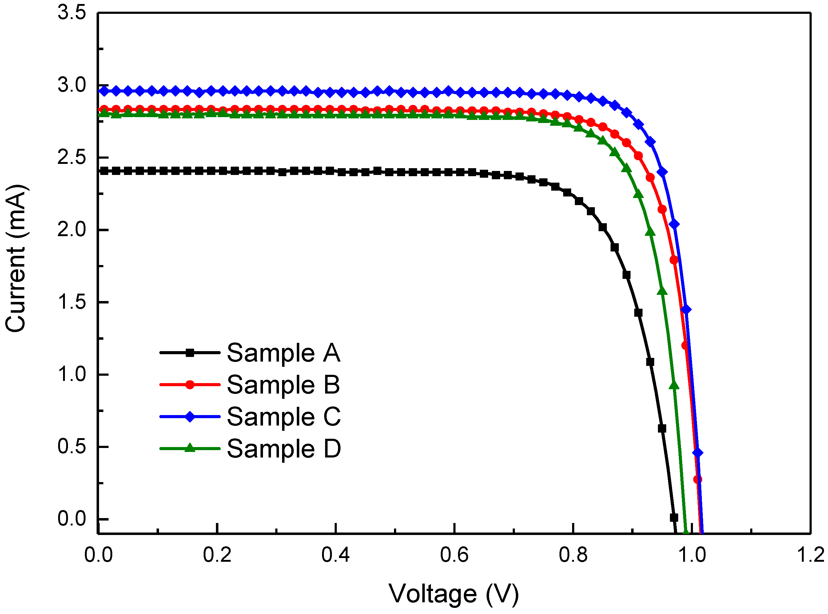
Figure 5 presents the I-V curves of the four samples under one sun condition by using an AM 1.5 solar simulator. The values of open-circuit voltage
Voc are obtained from the intersection of the I-V curve and the horizontal axis, and they are 0.97, 1.01, 1.02 and 0.99 V for samples A to D, respectively. The short-circuit currents
Isc for samples A to D are 2.41, 2.83, 2.96 and 2.79 mA, respectively, which are simply the device current at zero voltage. The maximum solar power
Pmax is estimated to be 1.79, 2.32, 2.50 and 2.22 mW for samples A to D, respectively, giving a power conversion efficiency
η of 15.5%, 20.0%, 21.6% and 19.2%. Sample C performs best, and this can be attributed to its highest short-circuit current
Isc (and therefore the highest induced photocurrent) due to the optimized grid spacing for effective light absorption and conversion to electric current. It may be noted that the solar performance in terms of
Pmax and
η for these samples is consistent with the LBIC measurement results of integrated photocurrent intensity presented previously. The consistency is not difficult to understand, because the solar illumination can be considered to be the amount of solar light beam incident at all positions on the sample surface at the same time. Although the LBIC light source is monochromatic, the integrated photocurrent intensity acquired in this study has managed to reflect the device’s solar performance to a significant extent.
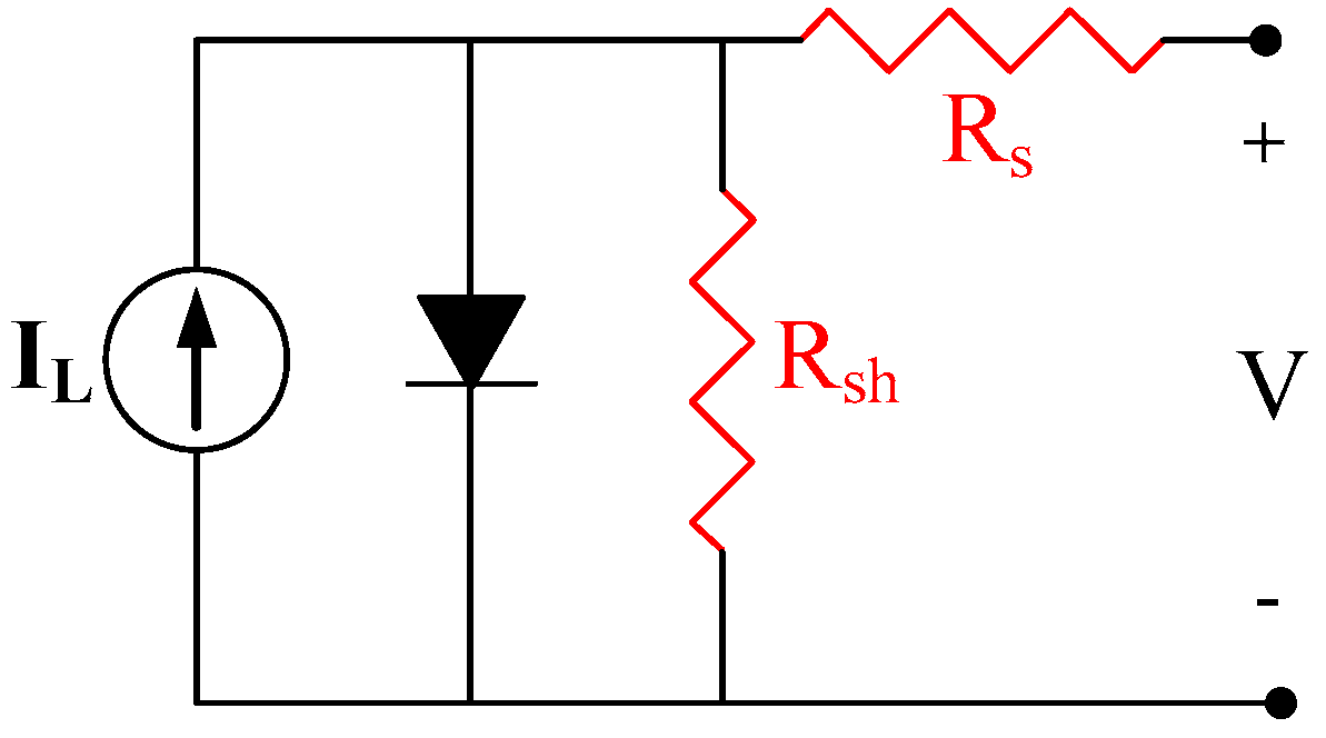
The equivalent circuit of a solar cell consisting of an ideal p-n diode, a photogenerated current source, and parasitic resistances (which most commonly are series resistance
Rs and shunt resistance
Rsh) is shown in
Figure 6. For an efficient solar cell, low
Rs and large
Rsh are beneficial for the fill factor
FF and thus the power conversion efficiency
η. The approximate values of
Rs and
Rsh can be extracted from the slopes of I-V curves at the open circuit and short circuit conditions, respectively. The results are listed in
Table 2. Given large values of
Rsh in this study, the ideality factor
n for our solar cell devices can be estimated through the simplified equation [
22]:
where
kB is the Boltzmann’s constant,
T is the absolute temperature,
q is the electron charge, and
I0 is the saturation current of the p-n diode. High
n values in solar cells tend to deteriorate the device’s solar characteristics.


