High-Responsivity Photovoltaic Photodetectors Based on MoTe2/MoSe2 van der Waals Heterojunctions


State Key Laboratory of New Ceramics and Fine Processing, School of Materials Science and Engineering, Tsinghua University, Beijing 100084, China
*
Author to whom correspondence should be addressed.
Crystals 2019, 9(6), 315; https://0-doi-org.brum.beds.ac.uk/10.3390/cryst9060315
Submission received: 4 June 2019
/
Revised: 16 June 2019
/
Accepted: 17 June 2019
/
Published: 19 June 2019
(This article belongs to the Special Issue Inorganic Layered Crystals: From Fundamentals to Materials Performance)
Abstract
:Van der Waals heterojunctions based on transition metal dichalcogenides (TMDs) show promising potential in optoelectronic devices, due to the ultrafast separation of photoexcited carriers and efficient generation of the photocurrent. Herein, this study demonstrated a high-responsivity photovoltaic photodetector based on a MoTe2/MoSe2 type-II heterojunction. Due to the interlayer built-in potential, the MoTe2/MoSe2 heterojunction shows obvious photovoltaic behavior and its photoresponse can be tuned by the gate voltage due to the ultrathin thickness of the heterojunction. This self-powered photovoltaic photodetector exhibits an excellent responsivity of 1.5 A W−1, larger than previously reported TMDs-based photovoltaic photodetectors. Due to the high-efficiency separation of electron-hole pairs and ultrafast charge transfer, the light-induced on/off ratio of current switching is larger than 104 at zero bias, and the dark current is extremely low (~10−13 A). These MoTe2/MoSe2 type-II heterojunctions are expected to provide more opportunities for future nanoscale optoelectronic devices.
1. Introduction
The recent advances in two-dimensional (2D) layered materials have provided brand-new platforms and thoughts for future novel, high-performance, and multi-functional electronic and optoelectronic applications. Of all these 2D materials, transition metal dichalcogenides (TMDs) including MoS2, WSe2, MoSe2, MoTe2, etc. have attracted a great deal of attention because of their peculiar characteristics, such as thickness-dependent bandgaps, valley-selective optical coupling, and large exciton binding energy [1,2]. Due to the lack of dangling bonds on the surface, heterojunctions can be assembled by any kinds of 2D materials through van der Waals (vdW) stacking without considering the lattice mismatch [3]. Recently, many novel physical phenomena and features are observed in these 2D-based vdW heterojunctions, including negative differential conductance, ultrafast carrier transport, interlayer excitons, moiré excitons, ballistic transport, etc. [4,5,6,7,8].
Depending on band structures of semiconductors, three types of heterojunctions can be obtained: Straddling gap (type-I), staggered (type-II), and broken gap (type-III). Among these heterojunctions, type-II junctions are superior candidates for optoelectronic devices, due to the high-efficiency separation of photoexcited carriers. In particular, type-II heterojunctions based on layered TMDs show promising potential in solar cells and photodetectors, due to their strong photon absorption, efficient generation of photocurrents, and ultrafast transfer of charges [9]. Furthermore, owing to the ultrathin thickness and steep interfacial charge-carrier gradient, 2D vdW heterojunctions exhibit distinct tunability in carrier density and band alignment, providing an alternative method for multi-functional electronic and optoelectronic devices. For instance, high external quantum efficiency (40–60%) is achieved in atomically thin GaTe/MoS2 and WSe2/MoS2 p-n heterojunctions [10,11]. On the other hand, gate-tunable photovoltaic response is also observed in WSe2/MoS2 heterojunctions [11,12], and photovoltaic photodetectors based on MoTe2/MoS2 vdW heterojunctions are also demonstrated [13,14,15]. However, the responsivity of these photovoltaic devices is still low (<0.5 A W−1), because of the small photocurrent flow without external bias driving. Therefore, more efforts are necessary to improve the performance of TMDs-based photovoltaic photodetectors for future nanoscale optoelectronic devices.
In this work, a high-responsivity photovoltaic photodetector based on a MoTe2/MoSe2 type-II vdW heterojunction is demonstrated. Due to the interlayer built-in potential, the MoTe2/MoSe2 heterojunction shows obvious photovoltaic behavior, and this photoresponse can be tuned by the gate voltage due to the ultrathin thickness of the heterojunction. This self-powered photodetector exhibits an excellent responsivity of 1.5 A W−1, larger than previously reported TMDs-based photodetectors. Due to the high efficiency of separation of electron-hole pairs and the ultrafast charge transfer, the light-induced on/off ratio of the current switching is larger than 104 at zero bias, and the dark current is extremely low (~10−13 A).
2. Materials and Methods
Device fabrication: The MoTe2/MoSe2 heterojunctions are fabricated by exfoliation and deterministic transfer methods. The few-layer MoTe2 and MoSe2 are exfoliated onto clean SiO2/Si substrate from MoTe2 and MoSe2 crystal (2D semiconductors Inc.) using scotch tape. Afterwards, the polymethyl methacrylate (PMMA) liquid is spin coated on the substrate with few-layer MoTe2 flakes with a rotating speed of 2000 r s−1. After annealed with 150 °C for 2 mins, the substrate with PMMA is soaked into the 1 mol L−1 KOH solution to remove the Si substrate. Then, the PMMA film with MoTe2 flakes is floated and transferred onto polydimethylsiloxane (PDMS) with MoTe2 flakes upside. After locating the appropriate thin MoTe2 flakes on the PMMA/PDMS film, the film with MoTe2/PMMA/PDMS structure is turned upside down and aligned with the target few-layer MoSe2 using a transfer stage under an optical microscope. Once the desired alignment is achieved, the MoTe2/PMMA/PDMS film structure is pressed against the substrate with MoSe2 compactly. Lastly, the substrate with MoTe2/MoSe2/PMMA/PDMS film structure is soaked into acetone to dissolve the PMMA in company with removing the PDMS and the stacked MoTe2/MoSe2 heterojunction is achieved. The contact electrodes were patterned by an electron beam lithography. Then, 20 nm Pt and 50 nm Au are deposited on MoTe2 and 20 nm Ti and 50 nm Au on MoSe2 by electron beam evaporation. After the liftoff process, the devices are annealed at 200 °C for 2 h in Ar/H2 (H2: 10%) atmosphere to remove the residual organics and improve the electrode contact between the semiconductor and metals. Herein, the MoTe2/MoSe2 heterojunctions are fabricated by the wet transfer process. In addition, dry transfer is also an alternative method to fabricate clean 2D devices [16].
Device characterization: Micro Raman spectra is measured by iHR550 spectrometer (HORIBA, Tokyo, Japan) with a 532 nm excitation wavelength. The thickness of materials are measured by an atomic force microscope (AFM, BRUKER Multimode 8, Germany) in contact mode using a silicon tip (on nitride lever). The surface potential is measured in the mode of a Kelvin probe force microscope (KPFM) with two scans, i.e., the morphology scan and interleave scan. During the interleave scan, the tip is lifted up and kept at an constant height over the sample surface based on the morphology scan. An alternating bias is applied on the tip to measure the surface potential of the sample. Electrical measurements are carried out on B1500A semiconductor device analyzer (KEYSIGHT, Santa Rosa, CA, USA) under an ambient environment in the dark and illumination condition (LED light source). The time-resolved photoresponse is also measured on B1500A under an illumination of LED light with the shutter switched between on and off for a period of 5 s.
3. Results and Discussion
3.1. Device Structure and Material Characterizations of MoTe2/MoSe2 Heterojunctions
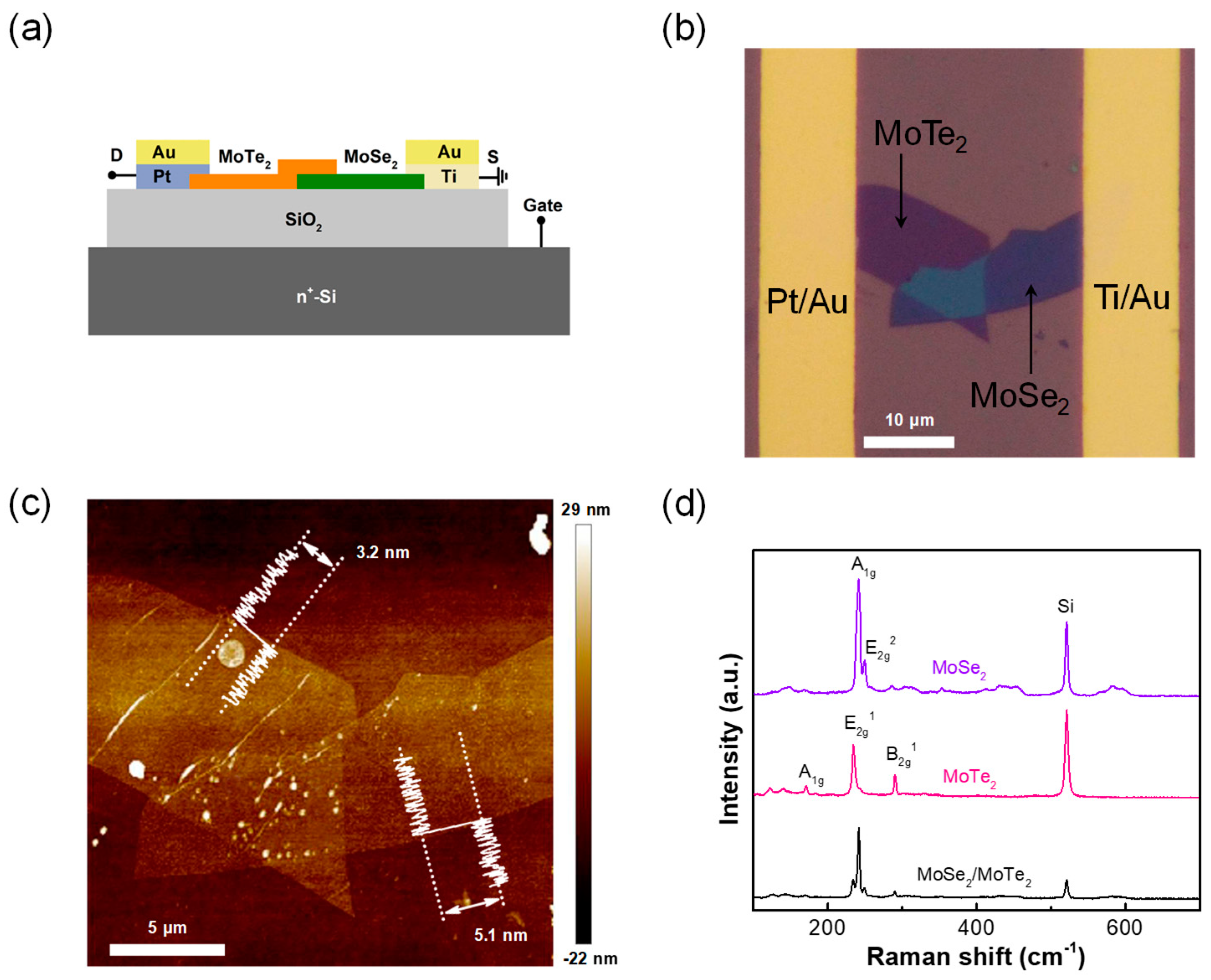
MoTe2/MoSe2 vdW heterojunctions are fabricated by mechanical exfoliation and deterministic transfer methods. Figure 1a shows the schematic of the MoTe2/MoSe2 heterojunction device. During electrical measurements, the source terminal (S) is grounded and the voltage is applied on the drain terminal (D) or n+-Si gate. An optical image of the MoTe2/MoSe2 device is displayed in Figure 1b. As MoTe2 layer has a smaller bandgap, to obtain good light absorption, the exfoliated few-layer MoTe2 flake is transferred on MoSe2 to form a heterojunction through vdW stacking. Metal Pt is deposited on MoTe2 layer to achieve good electrical contact and efficient holes injection. For MoSe2 layer, metal Ti is used as a contact electrode to ensure ohmic contact. The details on the device fabrication are depicted in the experimental section. According to the AFM results, the MoTe2 and MoSe2 thickness are 3.2 nm (~4 layer) and 5.1 nm (~7 layer), respectively, as shown in Figure 1c. Figure 1d shows the Raman spectra of a few-layered MoTe2 and MoSe2 nanoflakes as well as the overlapped junction zone. Two peaks are observed at 241.6 cm−1 and 249.8 cm−1 in the Raman spectra of MoSe2, which are attributed to out-of-plane vibrational mode A1g and two-phonon vibrational mode E2g 2 (a second-order Raman mode due to the longitudinal acoustic phonons at the M point in the Brillouin), respectively [17]. In the Raman spectra of MoTe2, three peaks appear at 171.8 cm−1, 234.9 cm−1, and 290.8 cm−1, corresponding to the out-of-plane vibrational mode A1g, in-plane vibrational mode E2g 1, and bulk in-active phonon vibrational mode B2g 1 [18]. In the MoTe2/MoSe2 heterojunction zone, the typical vibration peaks of both MoTe2 and MoSe2 are also observed, implying the existence of two different materials. In particular, the peak intensity of MoTe2 and MoSe2 in the overlapped region are attenuated, possibly due to the ultrafast charge transfer process in the MoTe2/MoSe2 vdW heterojunction [13].
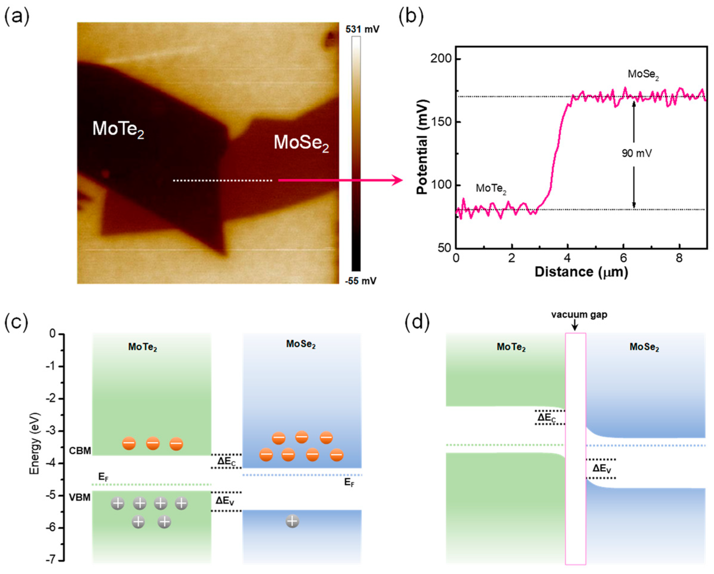
To verify the charge transfer and the existence of built-in potential at the interlayer of MoTe2/MoSe2 heterojunction under thermal equilibrium, KPFM measurements are conducted to qualitatively analyze the surface potential distribution. Figure 2a shows the KPFM map of the MoTe2/MoSe2 heterojunction, distinct potential difference is observed between MoTe2 and the MoSe2 region, and the potential of MoTe2 layer is lower than that of MoSe2 layer. The average surface potential difference between MoTe2 and MoSe2 layer is ~90 mV, as shown in Figure 2b, suggesting that the Fermi level of MoTe2 is 90 meV lower than MoSe2. This confirms the existence of a charge transfer and built-in potential at the heterojunction interlayer, which is the basis of a rectification heterojunction device. According to the reported band energy and the KPFM results, this study can obtain a schematic of band diagrams of MoTe2/MoSe2 before contact and after contact, as demonstrated in Figure 2c,d. Considering that it is difficult to quantitatively determine the width of the depletion region, the authors qualitatively analyzed the band bending of MoTe2 and MoSe2, and the thickness of materials, and the width of the depletion region are not considered exactly in Figure 2c,d. Unlike conventional heterojunctions, 2D heterojunctions are formed through vdW stacking, i.e., there are vdW gaps between two materials. Therefore, there is a vacuum band between MoTe2 and MoSe2 after contact. The conduction band minimum of a few-layered MoTe2 and MoSe2 are ~3.8 eV and ~4.1 eV, the bandgap of a few-layered MoTe2 and MoSe2 are 1.0–1.1 eV and 1.1–1.55 eV, respectively [19,20,21]. Therefore, a type-II vdW heterojunction is formed after the MoTe2 is stacked on MoSe2, which is beneficial for optoelectronic devices due to the high efficiency separation of photoexcited carriers. Herein, the MoTe2 and MoSe2 layer are intrinsically p-type and n-type doped. As the higher Fermi level of MoSe2, electrons (holes) will transfer from MoSe2 (MoTe2) to MoTe2 (MoSe2) until the equilibrium state is achieved. As a result, electrons (holes) depletion is formed at the MoSe2 (MoTe2) side. Thus, the energy bands of MoSe2 (MoTe2) bend upward (downward), as shown in Figure 2d. Due to the charge transfer, the built-in electric field at the heterojunction interlayer has a direction from MoSe2 to MoTe2.
3.2. Electrical Behaviors of MoTe2/MoSe2 Heterojunctions
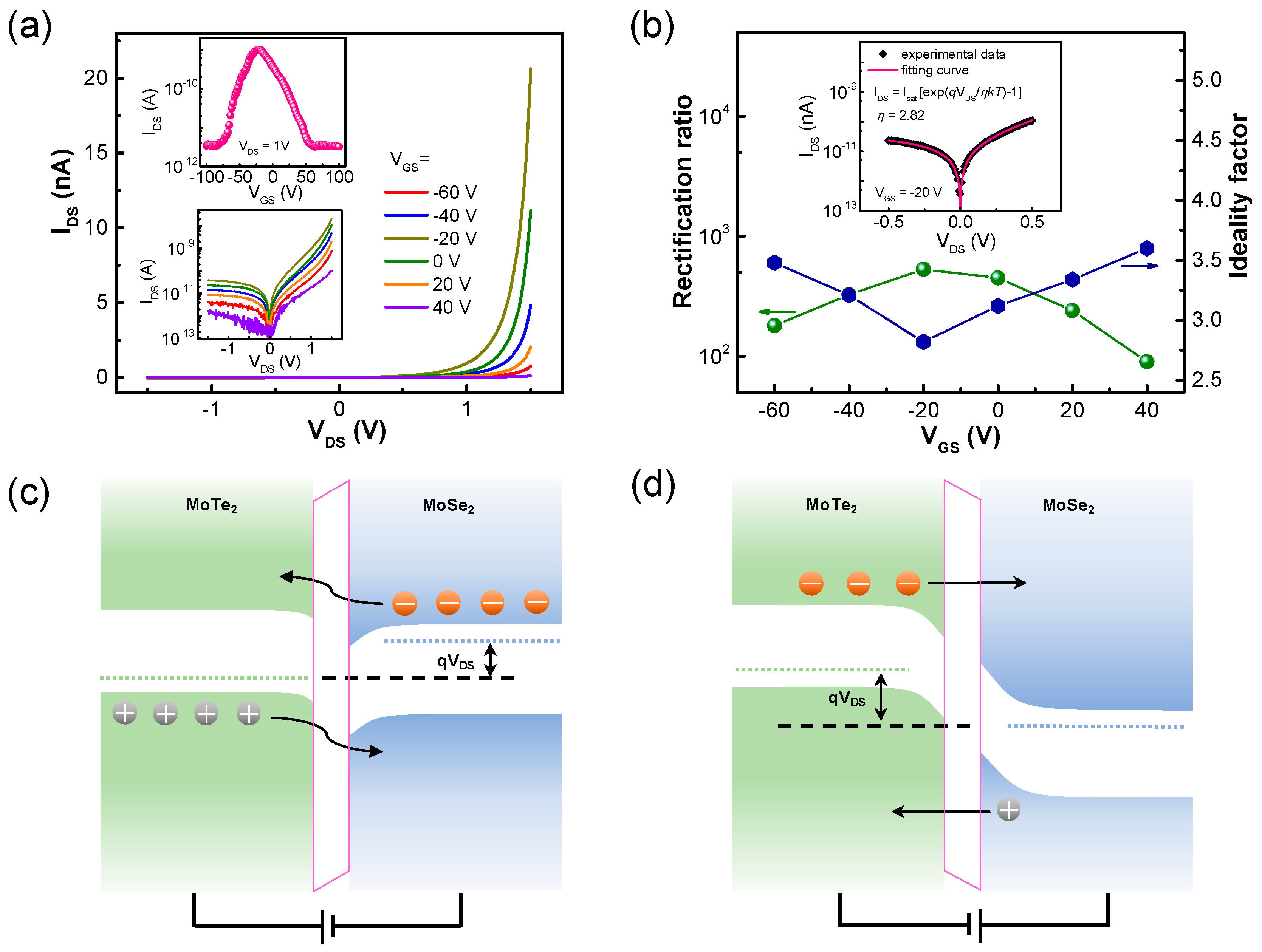
This study further investigated the electrical behavior of the MoTe2/MoSe2 heterojunctions. Figure 3a shows the linear scale of current-voltage (IDS-VDS) characteristics of MoTe2/MoSe2 heterojunction measured at different gate-source voltages (VGS). Two insets show the logarithmic scale of IDS-VDS curves and the transfer curve at VDS = 1V. The transfer curve shows an anti-ambipolar feature with a large on/off current ratio of ~300, which has also been observed in most 2D-based heterojunction devices [22,23]. The MoTe2/MoSe2 device exhibits distinct rectification behaviors at all VGS, demonstrating the gate-tunable current rectifying characteristics. Under VGS = −20 V, the heterojunction shows a large ratio of forward to reverse IDS ~ 540 at VDS = ± 1.5 V, which is better than most reported TMD-based heterojunctions [12,14]. The rectification ratio gradually decreases when VGS is larger or smaller than −20 V (Figure 3b), according with the anti-ambipolar feature of the transfer curve (inset of Figure 3a). Under a reverse bias, IDS displays exponential increases and finally saturates as VDS decreases. Under a forward bias, IDS shows exponential increases at low bias regions and linearly increases at a large bias due to the series resistance.
Figure 3c,d demonstrate the schematic band diagram of MoTe2/MoSe2 heterojunction at a forward and reverse bias. Under a forward bias, the equilibrium state of MoTe2/MoSe2 heterojunction is broken and the potential barrier at the interlayer becomes lower so that the carriers can easily be overcome. Electrons (holes) in the MoSe2 (MoTe2) are injected to the MoTe2 (MoSe2) side, leading to a large diffusion current in the heterojunction. The forward current will increase linearly when the applied bias is larger than the interlayer barrier height. On the contrary, under a negative bias, the interlayer barrier will increase. This increased built-in field will enhance the transport of minority carriers, forming a small reverse drift current. For heterojunctions based on 2D materials, the reverse current is mainly influenced by the surface trap effect, high level injection, series resistance, and the current generated in the barrier region. Of all these factors, the current generated in the barrier region should be the leading contributor in our MoTe2/MoSe2 heterojunctions. In the equilibrium state, the rate of carrier generation equals to the recombination by defect recombination centers in the space charge region. Under a reverse bias, the electron-hole pairs will be separated by the enhanced built-in field before they are recombined, forming a net generation rate. As the reverse bias increases, the increased net generation rate leads to the enhancement of a reverse current. Due to the ultra-thin feature of MoTe2/MoSe2 heterojunction, the width of the space charge region is equal to the thickness of the junction zone in the case of full depletion [14,24]. Therefore, the further increase of the reverse bias cannot enhance the built-in electric field due to the lack of mobile charges. Therefore, considering that there is a potential drop along the lateral region of the heterojunction, the increase of the reverse bias will result in a large lateral electric field, which can sweep the carriers away effectively, forming a large reverse current in the heterojunctions.
To further understand the electrical behavior of the MoTe2/MoSe2 heterojunctions, the ideality factor is extracted from the IDS-VDS curves at a low bias region, through fitting the IDS with the Shockley equation [25]:
where Isat is the reverse saturation current, q is the unit charge, η is the ideality factor, k is the Boltzmann constant, T is the absolute temperature. As displayed in the inset of Figure 3b, the measured IDS-VDS curve can be perfectly fitted by the Shockley equation, providing an ideality factor of 2.82 at VGS = −20 V. For ideal diodes, the ideality factor varies between 1.0 and 2.0, depending on the recombination of the minority carrier in the neutral region or space charge region of the junction. Nevertheless, the ideality factor is usually larger than 2.0 in experiments, which is suggested to be resulting from the interface diffusion, heterojunction interface with high strain, high series resistance or parasitic rectifying junction within the device [26,27,28]. For our MoTe2/MoSe2 heterojunction, the ideality factor may be mainly influenced by the lateral series resistance. As the ideality factor shows an increase trend when the VGS is larger or smaller than −20 V (Figure 3b), corresponding with the transfer characteristic (inset of Figure 3a), in which the lateral resistance (IDS) of the heterojunction increases (decreases) when VGS is larger or smaller than −20 V.
3.3. Opto-Electrical Behaviors of MoTe2/MoSe2 Heterojunctions
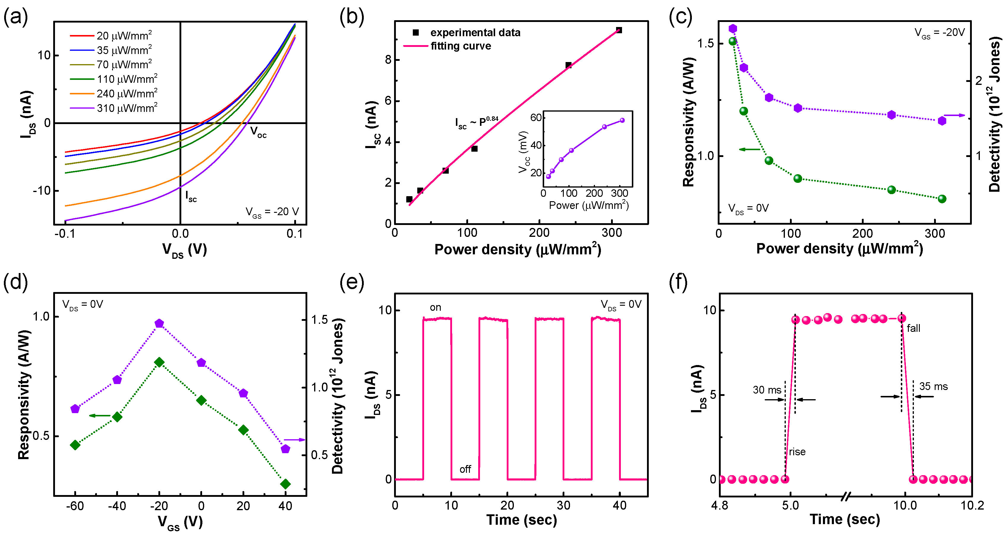
This study further investigated the optoelectronic characteristics of the MoTe2/MoSe2 heterojunctions. Figure 4a shows the IDS-VDS curves under a white light illumination (LED source), where IDS increases significantly with the increasing power density of the light. The device reveals a dramatic photovoltaic behavior, forming an open-circuit voltage (VOC) and a short-circuit current (ISC). The photovoltaic feature of the device results from the energy gradient in the type-II band alignment and the built-in electric field at the MoTe2/MoSe2 interlayer (Figure 1d), which can effectively separate the photoexcited electron-hole pairs. The photoexcited electrons and holes near the MoTe2/MoSe2 interlayer can be transferred to and accumulated at the MoSe2 and the MoTe2 side, respectively, leading to the formation of VOC. Once the device is short circuited, the accumulated electrons and holes at the two sides will recombine rapidly through the external circuit, leading to the formation of ISC. Figure 4b shows the ISC (i.e., current at zero external bias) as a function of light power density. The ISC strongly depends on the light intensity, and can be perfectly fitted by a power law equation ISC ~ αPβ, where α is a scaling constant, and β is an exponent [13]. Typically, a larger exponent value means a higher efficiency of the photoexcited electron-hole pairs under the light illumination. The fitting delivers an almost straight line with β = 0.84, which is slightly smaller than that of junctions with low interface trap states (β ~ 1) [29,30], indicating the presence of some trap states between the Fermi level and the conduction band edge and these trap states play a role in carriers generation and the recombination process [31]. The inset of Figure 4b shows the dependence of VOC on the power density. The VOC increases from 17.5 mV to 58.3 mV as the power density changes from 20 μW mm–2 to 310 μW mm−2. Theoretically, the open-circuit voltage is determined by the Fermi level difference (i.e., built-in potential) between two semiconductor materials. Herein, the maximum VOC is still smaller than the Fermi level difference (90 mV) between the MoTe2 and the MoSe2 layer as estimated by the KPFM measurements, suggesting that the performance of MoTe2/MoSe2 heterojunction may be further improved through optimizing the junction interface.
Owing to the photovoltaic effect, the MoTe2/MoSe2 heterojunctions can work as high-performance photovoltaic photodetectors. Therefore, this study evaluated the responsivity and the detectivity of the MoTe2/MoSe2 device at VDS = 0 V, i.e., the device always works in the low injection regime, as shown in Figure 4c. The responsivity is defined as R = Iph/Pin, in which Pin is the power of incident illumination, Iph is the photocurrent. Iph is calculated by equation: Iph = Iillum − Idark, where Iillum and Idark is the current measured under light illumination and dark conditions. The responsivity is estimated to be 0.81 A W−1 with a power density of 310 μW mm−2 at VGS = −20 V. Assuming the total noise is dominated by the shot noise from the dark current [32], the detectivity is defined by the equation, D = R / (2qJDS)1/2, where JDS is the density of dark current. The detectivity is estimated to be 1.47 × 10¹² Jones with a power density of 310 μW mm−2 at VGS = −20 V. As shown in Figure 4c, both the responsivity and detectivity can be further enhanced though reducing the light intensity, and a maximum responsivity and detectivity of 1.5 A W−1 and 2.7 × 10¹² Jones are obtained at a power density of 20 μW mm−2. This phenomenon might be due to the trap states on the material surface and at the heterojunction interlayer. Under a weak power density, the photoexcited electrons will be captured by the trap states, which reduces the recombination of carriers and augmenting the life-time of photoexcited holes, resulting a higher responsivity and detectivity [33]. With increasing power density, however, the available trap states will be reduced, leading to the saturation of photoresponse. The authors have also fabricated two other MoTe2/MoSe2 heterojunctions, which show a maximum responsivity of 1.39 and 1.65 A W−1, respectively, closing to the above MoTe2/MoSe2 device.
As our MoTe2/MoSe2 heterojunctions show gate-tunable rectification behavior, the photoresponse can be tuned by the gate votage, as shown in Figure 4d. The responsivity and detectivity achieve the maximum at VGS = −20 V and show a decreasing trend when VGS is smaller or larger than −20 V, in accordance with the gate-tunable rectification behavior and the anti-ambipolar feature. A similar gate-tunable photoresponse has also been observed in MoS2/WSe2 heterojunction devices, which display a photovoltaic responsivity of 0.011−0.12 A W−1 [11,12]. Figure 4e shows the temporal photoresponse of the MoTe2/MoSe2 device under the illumination of white light with a power density of 310 μW mm−2 at VDS = 0 V and VGS = −20 V. The photocurrent (i.e., ISC) can be generated and annihilated instantly with switching the light on and off, which shows an on/off ratio as high as 3.0 × 10⁴. The real response times at rise and fall should be less than 30 ms and less than 35 ms, respectively (Figure 4f), because the measured time interval between two adjacent data points are limited by the temporal resolution of the equipment. The fast response reveals a high-efficiency generation and separation of electron-hole pairs for the MoTe2/MoSe2 heterojunction.
The comparisons of figure of merits with other 2D photovoltaic photodetectors are shown in Table 1, where the responsivity, detectivity, and rise time are included. It is obvious that our MoTe2/MoSe2 photodetectors exhibit much higher responsivity in combination with high detectivity performance. The response speed of the MoTe2/MoSe2 photodetectors is comparable with part of the reported MoTe2/MoS2 heterojunctions and the MoTe2/CdS mixed-dimensional photodetectors, but slower than the GaSe/GaSb photodetectors.
4. Conclusions
Based on the intrinsic p-type MoTe2 and n-type MoSe2, this study fabricated MoTe2/MoSe2 p-n heterojunctions with type-II band alignment through van der Waals stacking. The electronic and optoelectronic performance of the devices have been investigated in detail. The MoTe2/MoSe2 heterojunction exhibits gate-tunable rectification behavior and a large rectification ratio of ~540, and an ideality factor of ~2.82 is achieved. Due to the type-II band alignment and the built-in potential at the interlayer, the MoTe2/MoSe2 heterojunction shows excellent photovoltaic effects with a photocurrent on/off ratio of >104. As a self-powered photovoltaic photodetector, the MoTe2/MoSe2 heterojunction shows a high responsivity of 1.5 A W−1 and a large detectivity of 2.7 × 10¹² Jones, featuring a high-performance, energy-efficient detector. These excellent performances suggest that the van der Waals heterojunctions have great potential in novel, high-performance electron and optoelectronic applications.
Author Contributions
H.L. and K.L. designed the experiments, analyzed the data, and wrote the manuscript. H.L. fabricated heterojunction devices, conducted the electrical and optoelectrical measurements. B.W. and E.W. carried out the AFM and KPFM measurements. Y.S. and X.W. performed the Raman spectra measurements. All authors commented on the manuscript.
Funding
This work was financially supported by National Natural Science Foundation of China (11774191) and Fok Ying-Tong Education Foundation (161042).
Conflicts of Interest
The authors declare no conflict of interest.
References
- Wang, Q.H.; Kalantar-Zadeh, K.; Kis, A.; Coleman, J.N.; Strano, M.S. Electronics and Optoelectronics of Two-Dimensional Transition Metal Dichalcogenides. Nat. Nanotechnol. 2012, 7, 699–712. [Google Scholar] [CrossRef] [PubMed]
- Jariwala, D.; Sangwan, V.K.; Lauhon, L.J.; Marks, T.J.; Hersam, M.C. Emerging Device Applications for Semiconducting Two-Dimensional Transition Metal Dichalcogenides. ACS Nano 2014, 8, 1102–1120. [Google Scholar] [CrossRef] [PubMed] [Green Version]
- Jariwala, D.; Marks, T.J.; Hersam, M.C. Mixed-dimensional Van der Waals Heterostructures. Nat. Mater. 2017, 16, 170–181. [Google Scholar] [CrossRef] [PubMed]
- Nourbakhsh, A.; Zubair, A.; Dresselhaus, M.S.; Palacios, T. Transport Properties of a MoS2/WSe2 Heterojunction Transistor and Its Potential for Application. Nano Lett. 2016, 16, 1359–1366. [Google Scholar] [CrossRef] [PubMed]
- Ceballos, F.; Bellus, M.Z.; Chiu, H.Y.; Zhao, H. Ultrafast Charge Separation and Indirect Exciton Formation in a MoS2-MoSe2 van der Waals Heterostructure. ACS Nano 2014, 8, 12717–12724. [Google Scholar] [CrossRef] [PubMed]
- Chen, H.L.; Wen, X.W.; Zhang, J.; Wu, T.M.; Gong, Y.J.; Zhang, X.; Yuan, J.T.; Yi, C.Y.; Lou, J.; Ajayan, P.M.; et al. Ultrafast Formation of Interlayer Hot Excitons in Atomically Thin MoS2/WS2 Heterostructures. Nat. Commun. 2016, 7, 12512. [Google Scholar] [CrossRef] [PubMed]
- Tran, K.; Moody, G.; Wu, F.C.; Lu, X.B.; Choi, J.; Kim, K.; Rai, A.; Sanchez, D.A.; Quan, J.M.; Singh, A.; et al. Evidence for Moire Excitons in van der Waals Heterostructures. Nature 2019, 567, 71–75. [Google Scholar] [CrossRef] [PubMed]
- Chen, S.W.; Han, Z.; Elahi, M.M.; Habib, K.M.M.; Wang, L.; Wen, B.; Gao, Y.D.; Taniguchi, T.; Watanabe, K.; Hone, J.; et al. Electron Optics with p-n Junctions in Ballistic Graphene. Science 2016, 353, 1522–1525. [Google Scholar] [CrossRef]
- Britnell, L.; Ribeiro, R.M.; Eckmann, A.; Jalil, R.; Belle, B.D.; Mishchenko, A.; Kim, Y.J.; Gorbachev, R.V.; Georgiou, T.; Morozov, S.V.; et al. Strong Light-Matter Interactions in Heterostructures of Atomically Thin Films. Science 2013, 340, 1311–1314. [Google Scholar] [CrossRef] [Green Version]
- Wang, F.; Wang, Z.X.; Xu, K.; Wang, F.M.; Wang, Q.S.; Huang, Y.; Yin, L.; He, J. Tunable GaTe-MoS2 van der Waals p-n Junctions with Novel Optoelectronic Performance. Nano Lett. 2015, 15, 7558–7566. [Google Scholar] [CrossRef]
- Lee, C.H.; Lee, G.H.; van der Zande, A.M.; Chen, W.C.; Li, Y.L.; Han, M.Y.; Cui, X.; Arefe, G.; Nuckolls, C.; Heinz, T.F.; et al. Atomically Thin p-n Junctions with van der Waals Heterointerfaces. Nat. Nanotechnol. 2014, 9, 676–681. [Google Scholar] [CrossRef] [PubMed]
- Furchi, M.M.; Pospischil, A.; Libisch, F.; Burgdorfer, J.; Mueller, T. Photovoltaic Effect in an Electrically Tunable van der Waals Heterojunction. Nano Lett. 2014, 14, 4785–4791. [Google Scholar] [CrossRef] [PubMed]
- Wang, B.; Yang, S.X.; Wang, C.; Wu, M.H.; Huang, L.; Liu, Q.; Jiang, C.B. Enhanced Current Rectification and Self-Powered Photoresponse in Multilayer p-MoTe2/n-MoS2 van der Waals Heterojunctions. Nanoscale 2017, 9, 10733–10740. [Google Scholar] [CrossRef] [PubMed]
- Chen, Y.; Wang, X.D.; Wu, G.J.; Wang, Z.; Fang, H.H.; Lin, T.; Sun, S.; Shen, H.; Hu, W.D.; Wang, J.L.; et al. High-Performance Photovoltaic Detector Based on MoTe2/MoS2 Van der Waals Heterostructure. Small 2018, 14, 1703293. [Google Scholar] [CrossRef] [PubMed]
- Pezeshki, A.; Hossein, S.; Shokouh, H.; Nazari, T.; Oh, K.; Im, S. Electric and Photovoltaic Behavior of a Few-Layer α-MoTe2/MoS2 Dichalcogenide Heterojunction. Adv. Mater. 2016, 28, 3216–3222. [Google Scholar] [CrossRef] [PubMed]
- Choi, K.; Lee, Y.T.; Min, S.W.; Lee, H.S.; Nam, T.; Kim, H.; Im, S. Direct Imprinting of MoS2 Flakes on a Patterned Gate for Nanosheet Transistors. J. Mater. Chem. C 2013, 1, 7803–7807. [Google Scholar] [CrossRef]
- Nam, D.; Lee, J.U.; Cheong, H. Excitation Energy Dependent Raman Spectrum of MoSe2. Sci. Rep. 2015, 5, 17113. [Google Scholar] [CrossRef] [PubMed]
- Lezama, I.G.; Arora, A.; Ubaldini, A.; Barreteau, C.; Giannini, E.; Potemski, M.; Morpurgo, A.F. Indirect-to-Direct Band Gap Crossover in Few-Layer MoTe2. Nano Lett. 2015, 15, 2336–2342. [Google Scholar] [CrossRef]
- Kang, J.; Tongay, S.; Zhou, J.; Li, J.B.; Wu, J.Q. Band Offsets and Heterostructures of Two-Dimensional Semiconductors. Appl. Phys. Lett. 2013, 102, 012111. [Google Scholar] [CrossRef]
- Tongay, S.; Zhou, J.; Ataca, C.; Lo, K.; Matthews, T.S.; Li, J.B.; Grossman, J.C.; Wu, J.Q. Thermally Driven Crossover from Indirect toward Direct Bandgap in 2D Semiconductors: MoSe2 versus MoS2. Nano Lett. 2012, 12, 5576–5580. [Google Scholar] [CrossRef]
- Ruppert, C.; Aslan, O.B.; Heinz, T.F. Optical Properties and Band Gap of Single- and Few-Layer MoTe2 Crystals. Nano Lett. 2014, 14, 6231–6236. [Google Scholar] [CrossRef] [PubMed]
- Li, Y.T.; Wang, Y.; Huang, L.; Wang, X.T.; Li, X.Y.; Deng, H.X.; Wei, Z.M.; Li, J.B. Anti-Ambipolar Field-Effect Transistors Based On Few-Layer 2D Transition Metal Dichalcogenides. ACS Appl. Mater. Inter. 2016, 8, 15574–15581. [Google Scholar] [CrossRef] [PubMed]
- Wang, F.; Yin, L.; Wang, Z.X.; Xu, K.; Wang, F.M.; Shifa, T.A.; Huang, Y.; Jiang, C.; He, J. Configuration-Dependent Electrically Tunable Van der Waals Heterostructures Based on MoTe2/MoS2. Adv. Funct. Mater. 2016, 26, 5499–5506. [Google Scholar] [CrossRef]
- Liu, Y.; Weiss, N.O.; Duan, X.D.; Cheng, H.C.; Huang, Y.; Duan, X.F. Van der Waals Heterostructures and Devices. Nat. Rev. Mater. 2016, 1, 16042. [Google Scholar] [CrossRef]
- Shockley, W. The Theory of P-N Junctions in Semiconductors and P-N Junction Transistors. Bell Syst. Tech. J. 1949, 28, 435–489. [Google Scholar] [CrossRef]
- Hao, J.H.; Gao, J.; Wang, Z.; Yu, D.P. Interface Structure and Phase of Epitaxial SrTiO3 (110) Thin Films Grown Directly on Silicon. Appl. Phys. Lett. 2005, 87, 131908. [Google Scholar] [CrossRef]
- Yang, Z.B.; Huang, W.; Hao, J.H. Determination of Band Alignment of Pulsed-Laser-Deposited Perovskite Titanate/III-V Semiconductor Heterostructure using X-ray and Ultraviolet Photoelectron Spectroscopy. Appl. Phys. Lett. 2013, 103, 031919. [Google Scholar] [CrossRef]
- Schein, F.L.; von Wenckstern, H.; Grundmann, M. Transparent p-CuI/n-ZnO Heterojunction Diodes. Appl. Phys. Lett. 2013, 102, 092109. [Google Scholar] [CrossRef]
- Zeng, L.H.; Wang, M.Z.; Hu, H.; Nie, B.; Yu, Y.Q.; Wu, C.Y.; Wang, L.; Hu, J.G.; Xie, C.; Liang, F.X.; et al. Monolayer Graphene/Germanium Schottky Junction as High-Performance Self-Driven Infrared Light Photodetector. ACS Appl. Mater. Inter. 2013, 5, 9362–9366. [Google Scholar] [CrossRef]
- Wu, D.; Jiang, Y.; Zhang, Y.G.; Li, J.W.; Yu, Y.Q.; Zhang, Y.P.; Zhu, Z.F.; Wang, L.; Wu, C.Y.; Luo, L.B.; et al. Device Structure-Dependent Field-Effect and Photoresponse Performances of p-type ZnTe:Sb Nanoribbons. J. Mater. Chem. 2012, 22, 6206–6212. [Google Scholar] [CrossRef]
- Kung, S.C.; van der Veer, W.E.; Yang, F.; Donavan, K.C.; Penner, R.M. 20 μs Photocurrent Response from Lithographically Patterned Nanocrystalline Cadmium Selenide Nanowires. Nano Lett. 2010, 10, 1481–1485. [Google Scholar] [CrossRef] [PubMed]
- Choi, W.; Cho, M.Y.; Konar, A.; Lee, J.H.; Cha, G.B.; Hong, S.C.; Kim, S.; Kim, J.; Jena, D.; Joo, J.; et al. High-Detectivity Multilayer MoS2 Phototransistors with Spectral Response from Ultraviolet to Infrared. Adv. Mater. 2012, 24, 5832–5836. [Google Scholar] [CrossRef] [PubMed]
- Xu, H.; Wu, J.X.; Feng, Q.L.; Mao, N.N.; Wang, C.M.; Zhang, J. High Responsivity and Gate Tunable Graphene-MoS2 Hybrid Phototransistor. Small 2014, 10, 2300–2306. [Google Scholar] [CrossRef] [PubMed]
- Ahn, J.; Jeon, P.J.; Raza, S.R.A.; Pezeshki, A.; Min, S.W.; Hwang, D.K.; Im, S. Transition Metal Dichalcogenide Heterojunction PN Diode toward Ultimate Photovoltaic Benefits. 2D Mater. 2016, 3, 045011. [Google Scholar] [CrossRef]
- Wang, P.; Liu, S.S.; Luo, W.J.; Fang, H.H.; Gong, F.; Guo, N.; Chen, Z.G.; Zou, J.; Huang, Y.; Zhou, X.H.; et al. Arrayed Van Der Waals Broadband Detectors for Dual-Band Detection. Adv. Mater. 2017, 29, 1604439. [Google Scholar] [CrossRef] [PubMed]
- Lu, M.Y.; Chang, Y.T.; Chen, H.J. Efficient Self-Driven Photodetectors Featuring a Mixed-Dimensional van der Waals Heterojunction Formed from a CdS Nanowire and a MoTe2 Flake. Small 2018, 14, 1802302. [Google Scholar] [CrossRef] [PubMed]
- Pospischil, A.; Furchi, M.M.; Mueller, T. Solar-energy Conversion and Light Emission in an Atomic Monolayer p-n Diode. Nat. Nanotechnol. 2014, 9, 257–261. [Google Scholar] [CrossRef] [PubMed]
Figure 1.
The schematic and characterizations of MoTe2/MoSe2 heterojunctions. (a) Schematic of the MoTe2/MoSe2 heterojunction device. During electrical measurements, the source terminal (S) is grounded while the bias is applied on the drain terminal (D) or Si gate. (b) An optical image of the MoTe2/MoSe2 heterojunction, in which the MoTe2 is stacked on the MoSe2. (c) AFM image of the MoTe2/MoSe2 heterojunction, the thickness of MoTe2 and MoSe2 are 3.2 and 5.1 nm, respectively. (d) Raman spectra of MoTe2, MoSe2, and MoTe2/MoSe2 heterojunction zone.

Figure 2.
The surface potential distribution and energy band diagrams of MoTe2/MoSe2 heterojunction. (a) KPFM image of the MoTe2/MoSe2 heterojunction. (b) Dependence of potential on the distance along the white dotted line marked zone in Figure 2a, providing a potential difference of 90 mV. (c) The schematic of a band diagram of isolated MoTe2 and MoSe2 (i.e., before contact). CBM, VBM, ΔEC, ΔEV, and EF denote the conduction band minimum, valence band maximum, conduction band offset, valence band offset, and Fermi level. (d) The schematic of a band diagram of the MoTe2/MoSe2 (i.e., after contact).

Figure 3.
Electrical characteristics of MoTe2/MoSe2 heterojunction and related band diagrams. (a) IDS-VDS characteristics in linear scale measured at different gate voltage VGS. Two insets show the logarithmic scale of IDS-VDS curves and the transfer curve at VDS = 1V. (b) The dependence of the rectification ratio and ideality factor on VGS. The inset shows the fitting of the IDS-VDS characteristic with the Shockley equation for the extraction of the ideality factor. The band diagram of carrier transport mechanisms of the MoTe2/MoSe2 heterojunction under (c) forward bias and (d) reverse bias.

Figure 4.
The photoresponse of MoTe2/MoSe2 heterojunction. (a) IDS-VDS characteristics of the MoTe2/MoSe2 heterojunction under white light illumination with different power density, showing dramatic photovoltaic effect. (b) ISC as a function of light power density, which can be fitted by a power law equation. The inset shows dependence of VOC on the power density. (c) The responsivity and detectivity of the MoTe2/MoSe2 heterojunction as a function of power density. (d) The responsivity and detectivity of the MoTe2/MoSe2 heterojunction as a function of VGS. (e) The time response of the MoTe2/MoSe2 heterojunction with incident light switches on and off for a period of 5 s at VDS = 0 V, demonstrating a self-driven behavior and high-efficient separation of photoexcited carriers. (f) The enlarged dynamic time response behavior of the MoTe2/MoSe2 heterojunction, suggesting a fast rise time (<30 ms) and fall time (<35 ms).


Table 1.
Comparisons of figure of merits of MoTe2/MoSe2 photodetector with other photovoltaic photodetectors. Gr, graphene.
Table 1.
Comparisons of figure of merits of MoTe2/MoSe2 photodetector with other photovoltaic photodetectors. Gr, graphene.
| Materials | Responsivity (A W−1) | Detectivity (Jones) | trise (ms) |
|---|---|---|---|
| MoTe2/MoS2 [13,14,15] | 0.046–0.32 | 1.06 × 10⁸ | 0.06–68 |
| WSe2/MoS2 [11,12,34] | 0.011–0.25 | ||
| GaSe/GaSb [35] | 0.12 | 2.2 × 10¹² | 0.032 |
| MoTe2/CdS [36] | <0.06 | <50 | |
| Gr/WS2/Gr [9] | 0.1 | ||
| WSe2 p-n [37] | <0.016 | ||
| This work | 1.5 | 2.7 × 10¹² | <30 |
© 2019 by the authors. Licensee MDPI, Basel, Switzerland. This article is an open access article distributed under the terms and conditions of the Creative Commons Attribution (CC BY) license (http://creativecommons.org/licenses/by/4.0/).
Share and Cite
MDPI and ACS Style
Luo, H.; Wang, B.; Wang, E.; Wang, X.; Sun, Y.; Liu, K. High-Responsivity Photovoltaic Photodetectors Based on MoTe2/MoSe2 van der Waals Heterojunctions. Crystals 2019, 9, 315. https://0-doi-org.brum.beds.ac.uk/10.3390/cryst9060315
AMA Style
Luo H, Wang B, Wang E, Wang X, Sun Y, Liu K. High-Responsivity Photovoltaic Photodetectors Based on MoTe2/MoSe2 van der Waals Heterojunctions. Crystals. 2019; 9(6):315. https://0-doi-org.brum.beds.ac.uk/10.3390/cryst9060315
Chicago/Turabian StyleLuo, Hao, Bolun Wang, Enze Wang, Xuewen Wang, Yufei Sun, and Kai Liu. 2019. "High-Responsivity Photovoltaic Photodetectors Based on MoTe2/MoSe2 van der Waals Heterojunctions" Crystals 9, no. 6: 315. https://0-doi-org.brum.beds.ac.uk/10.3390/cryst9060315
Note that from the first issue of 2016, this journal uses article numbers instead of page numbers. See further details here.