High-Density Well-Aligned Dislocations Introduced by Plastic Deformation in Bi1−xSbx Topological Insulator Single Crystals


Institute of Industrial Science, The University of Tokyo, Komaba, Meguro-ku, Tokyo 153-8505, Japan
*
Author to whom correspondence should be addressed.
Crystals 2019, 9(6), 317; https://0-doi-org.brum.beds.ac.uk/10.3390/cryst9060317
Submission received: 24 May 2019
/
Revised: 13 June 2019
/
Accepted: 16 June 2019
/
Published: 19 June 2019
(This article belongs to the Section Crystal Engineering)
Abstract
:Topological insulators (TIs) have a bulk bandgap and gapless edge or surface states that host helically spin-polarized Dirac fermions. Theoretically, it has been predicted that gapless states could also be formed along dislocations in TIs. Recently, conductivity measurements on plastically deformed bismuth antimony (Bi1−xSbx) TIs have revealed excess conductivity owing to dislocation conduction. For further application of them, fundamental study on dislocations in TIs is indispensable. Dislocations controlled based on fundamental studies could potentially be useful not only for experimental investigations of the dislocation properties but also for diverse device applications. In the present study, Bi1−xSbx TI single crystals were fabricated by a zone-melting method. The crystals were plastically deformed at room temperature. The resultant dislocations were observed by transmission electron microscopy (TEM). It was found that high-density dislocations with the Burgers vector satisfying the condition for the formation of gapless states were successfully introduced. The dislocations were mostly of edge type with lengths on the order of more than a few micrometers.
1. Introduction
Topological insulators (TIs) are characterized by a bulk bandgap and necessarily highly conducting gapless edge or surface states that host helically spin-polarized Dirac fermions [1,2]. These gapless states are protected by time reversal symmetry. Therefore, they are robust against disorder scattering. The verification of three-dimensional (3D) TIs has attracted major attention to the physical properties of surface gapless states. In addition, it has been theoretically shown that gapless states could also be formed along dislocations in 3D TIs satisfying the following condition [3]:
where is the Burgers vector of the dislocation, () are the three of the four Z2 invariants () of the 3D TI [4,5], and () are the reciprocal basis vectors. 3D TIs are characterized by four Z2 topological invariants (). The first invariant, , defines strong or weak TIs, where corresponds to strong TI (STI) and corresponds to weak TI (WTI). In the case of STI, an odd number of Dirac mode(s) exists on the surface Brillouin zone (BZ) and , including the latter three invariants, , , and , indicates the location of the Dirac point(s) in the surface BZ. On the other hand, WTI is considered as layers of two-dimensional (2D) TI stacked along . When the condition in Equation (1) is satisfied, the surface Dirac particles acquire a π phase shift on crossing the dislocation. Consequently, a topologically protected gapless state is formed along the dislocation.
Similarly to edge states of 2D TIs, which are considered as guided propagation paths of electrons, the dislocations with gapless states are expected to carry dissipationless current. In addition, at high densities of such dislocations, the thermoelectric figure of merit ZT of TI materials can be dominated by one-dimensional (1D) topologically protected conducting states channeled through the dislocations [6]. Thus, the dislocation with gapless states is a candidate for applications in electronic and thermoelectric devices. It should be noted that, in order to satisfy the condition in Equation (1), at least one of the latter three invariants, , , or , must be 1. However, most of the TIs discovered so far, including some of the most-intensively studied (Bi,Sb)2(S,Se,Te)3 tetradymites, exhibit band inversion at the Γ point; thus, they are classified with the invariants (1;000) [2], where no 1D gapless states along the dislocations can be realized. In contrast, bismuth antimony (Bi1-xSbx) TI exhibit band inversion at the L points, and has the invariants (1;111) [7,8]. Thus, it is one of the limited candidates for realization of 1D gapless states along the dislocations.
A Bi1−xSbx solid solution is formed in all compositions of 0 < x < 1. The electronic band structure is drastically modified depending on the composition. It has been known that the solid solution becomes a semiconductor in the composition range 0.07 < x < 0.22 [9]. In 2006, the semiconductor was predicted to be a TI with the invariants (1;111) [7], which was experimentally verified in the following year [8]. As for the conducting dislocations in TIs, while several theoretical studies have been reported [10,11,12], no experimental investigations have been reported until recently [13]. Hamasaki et al. performed conductivity measurements on plastically deformed Bi1−xSbx TI, which exhibited excess conductivity owing to dislocation conduction [13]. For further use of them in applications, a fundamental study on dislocations in TIs is indispensable. Dislocations controlled based on fundamental studies could potentially be useful not only for experimental investigations of the dislocation properties, but also for diverse device applications.
Bi1−xSbx belongs to the rhombohedral A7 structure. Concerning dislocations in Bi1-xSbx, the report by Hamasaki et al. [13] is the first and the only one so far. Regarding Bi that has the same crystal structure as Bi1−xSbx, some studies that used the etch pit method on the dislocations introduced by plastic deformation have been reported [14,15]. However, there are no reports on transmission electron microscopy (TEM) observations of dislocations in Bi, which is mainly due to the difficulty of TEM specimen fabrication, i.e., Bi has a large atomic number; therefore, thinner specimens are required to achieve electron transparency compared to materials with smaller atomic numbers.
In the present study, Bi1−xSbx TI single crystals were fabricated by a zone-melting method. The crystals were plastically deformed at room temperature. The resultant dislocations were observed by TEM to reveal the substructure, density, and Burgers vectors.
2. Materials and Methods
Bi1−xSbx single crystals were grown by a zone-melting method. First, a mixture of high-purity (6N) Bi and Sb elements, with an Sb concentration of x = 0.10, was sealed in an evacuated quartz ampoule with a 7 mm inner diameter. Then, the material was melted and homogenized at 400–450 °C, followed by quenching in ice water. Subsequently, the ingot was subjected to zone melting for crystal growth by using a four mirror infrared furnace (FZ-T-10000-H-HR-TUM-VM-PC, Crystal Systems Co., Ltd., Yamanashi, Japan). The growth velocity was set at 0.1 mm/h to avoid constitutional supercooling resulting in the segregation of Sb. The grown crystal was cut in half along the growth direction to obtain a flat surface. Then, the compositions of the grown crystals were investigated by an electron probe microanalyzer (EPMA) (JXA-8800RL, JEOL Ltd., Tokyo, Japan). For quantitative composition analyses, a melt-spun Bi0.9Sb0.1 sample, produced by a single-roller method, was used as a standard for ZAF conversion from the intensities of Bi Lα1 and Sb Lα1 to concentrations, where Z is the atomic number factor, A is the absorption factor, and F is the fluorescence factor.
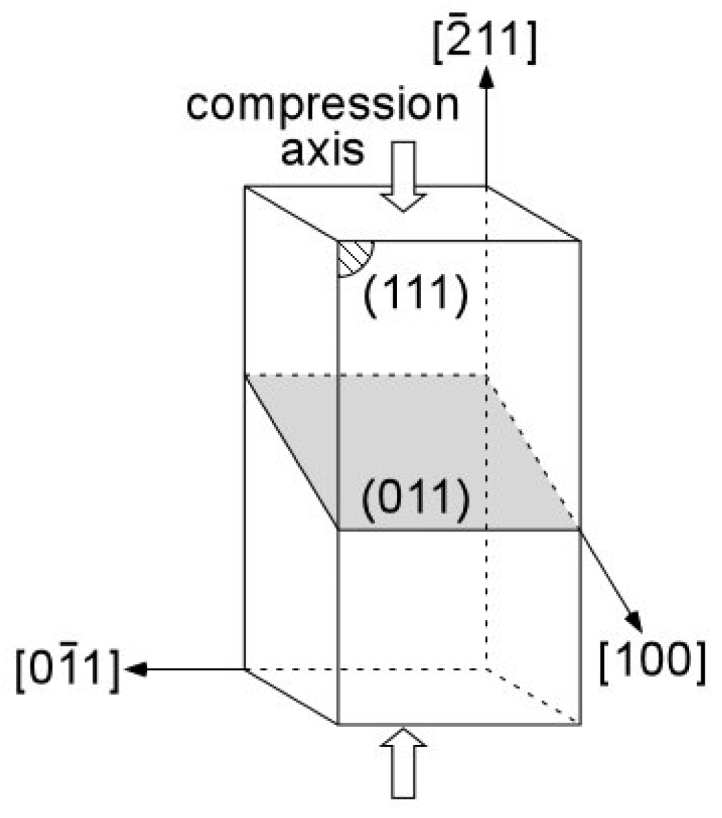
Rectangular samples approximately 1 × 1 × 2 mm3 in size were cut out and used for the deformation tests. The compression axis and the strain rate were carefully chosen so as to introduce dislocations satisfying the condition in Equation (1). Figure 1 shows the crystallographic orientations of the samples for deformation. The compression axis was set to the direction, in which the primary slip system is sufficiently suppressed. According to a previous study that used the etch pit method on the dislocations, which were introduced by plastic deformation of Bi [15], the slip system should be activated with the orientation relationship shown in Figure 1, where the Schmid factor for the slip system and the primary slip systems is 0.46 and 0, respectively. Here, it should be noted that satisfies Equation (1), while does not. Although the . direction is another possible compression axis to activate the slip system [13,15], the direction is advantageous to activate a single slip system . In our previous study [13], the compression axis was the direction declined by a few degrees from the direction toward the direction, where a single slip system out of the three equivalent slip systems of is activated. However, with the compression axis, as the deformation proceeds, the possibility that other two equivalent slip systems, and , are activated increases. Therefore, we consider that the direction is better than the direction to activate a single slip system out of the three equivalent slip systems of . The strain rate was set to be approximately 1 × 10⁻⁵ s−1 to avoid twin formation. Twinning deformation easily occurs at a strain rate of 1 × 10⁻³ s−1 [16,17] and is suppressed at a strain rate of 1 × 10⁻⁴ s−1 or lower [15,18]. The rectangular samples were deformed by compression at room temperature up to 10%.
The deformed samples were examined by TEM (JEM-2010F, 2010HC, 200 kV, JEOL Ltd., Tokyo, Japan) to identify the substructure, density, and the Burgers vector of the introduced dislocations. The TEM specimens were cut out along the plane and the plane of the deformed samples, and these were further prepared by mechanical thinning and Ar ion milling.
3. Results and Discussion
3.1. Crystal Growth
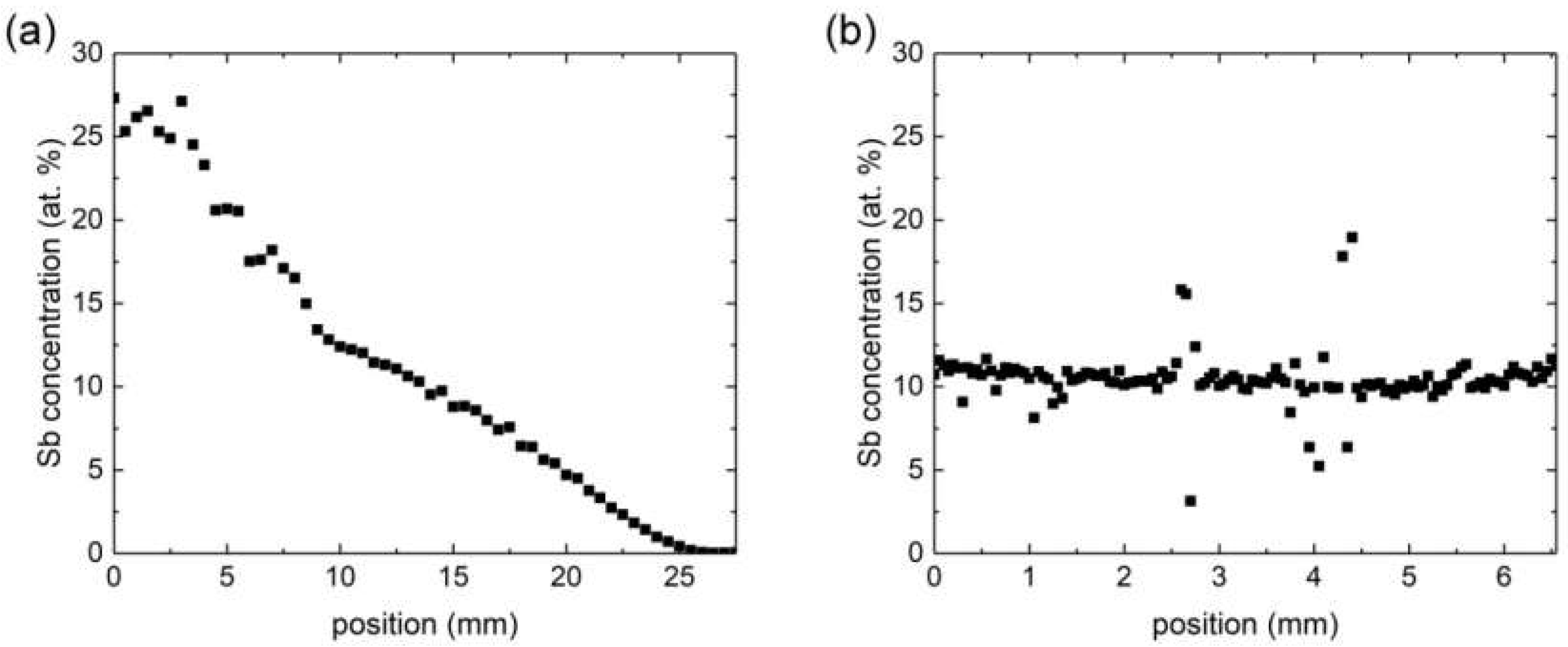
The grown crystal, 27.5 mm in length and 7 mm in diameter, contained two grain boundaries along the growth direction. Figure 2a,b shows the EPMA line profiles of Sb concentrations obtained for the grown crystal. The line profile in Figure 2a was obtained along the crystal growth direction. In the region between 4.5 mm and 17.5 mm from the tip, the crystal was within the range of the TI phase, 0.07 < x < 0.22. The line profile in Figure 2b was perpendicular to the growth direction at a position of 13.5 mm from the tip of the grown crystal. Obvious jumps in the profile corresponded to cavities around the grain boundaries. The radial variation in the Sb concentration was about 2%. Sb concentrations were lower in the center of the crystal than in its outer regions, which could be due to the radial temperature gradient during crystal growth.
3.2. Plastic Deformation
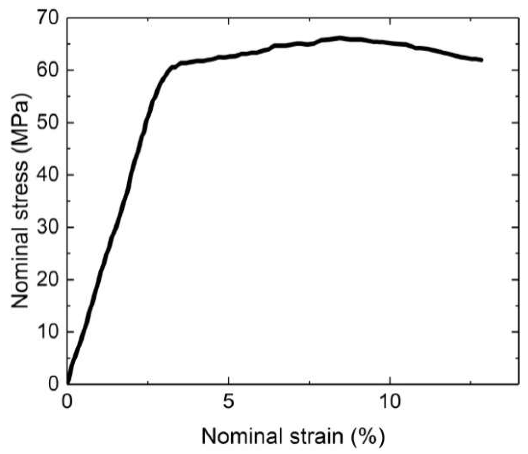
Figure 3 shows the stress–strain curve obtained from the sample with an Sb concentration in the range of 8.6–9.8 at%. The yield stress was about 60 MPa. This value was an order of magnitude higher than that for the deformation of Bi at room temperature [15,18,19,20]. This result is consistent with the fact that the interatomic distance of the Bi1-xSbx solid solution becomes shorter with increasing Sb concentrations. Work hardening behavior was slightly observed during the initial stage of plastic deformation. Slip traces parallel to the direction were observed on the surface of the deformed samples. In our previous study [13], where the compression axis declined a few degrees from the direction, obvious work hardening was observed, indicating that possibly more than one equivalent slip systems were activated.
3.3. TEM Observations of Dislocations Introduced by Plastic Deformation
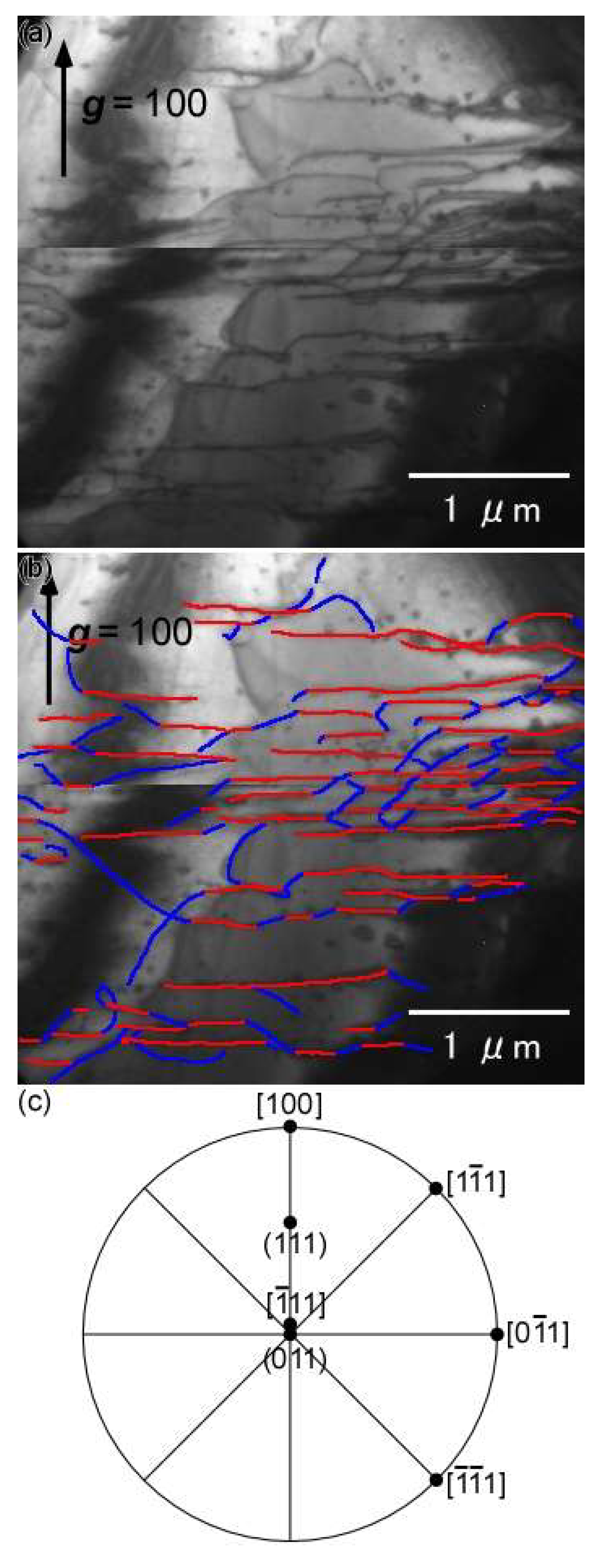
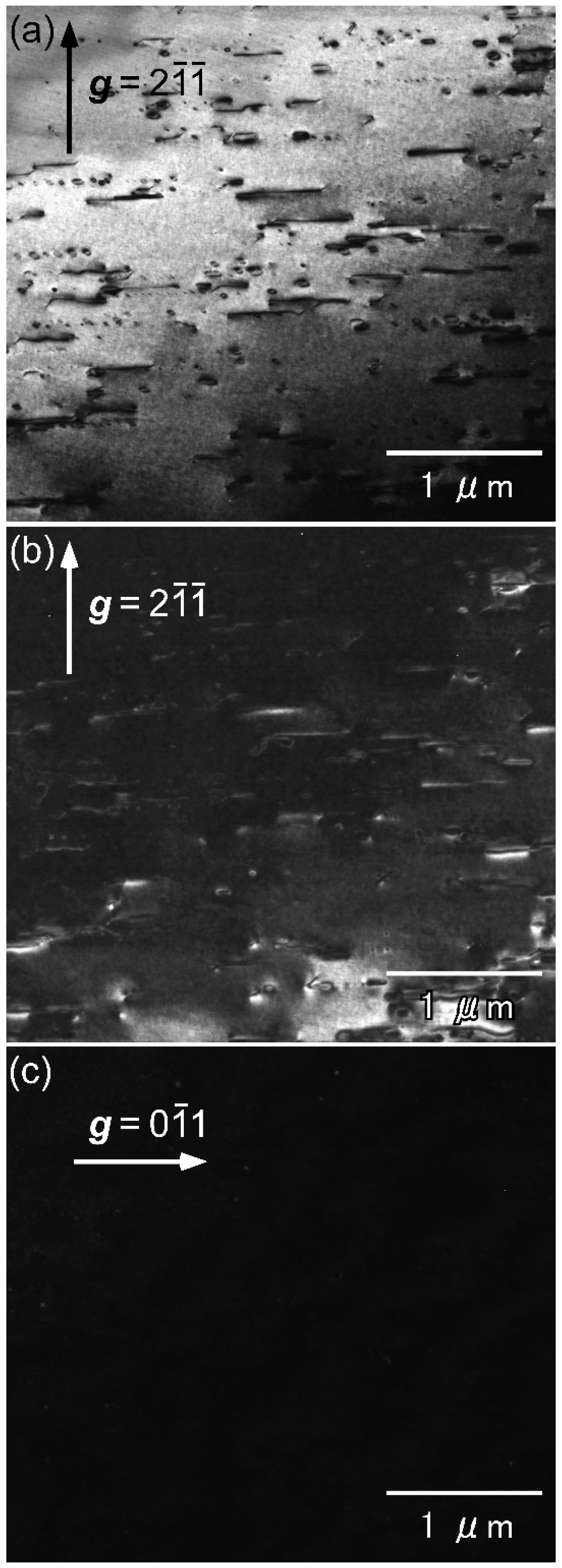
Figure 4a shows typical TEM bright-field images obtained from the slip plane of the deformed sample. The observation direction was tilted from the normal direction of the slip plane by approximately . Using the convergent-beam technique, the thickness of the TEM specimen was determined to be approximately 100 nm. The total dislocation length observed in the area of 12 μm2 in Figure 4a was approximately 50 μm. The dislocation density in that area was estimated to be . From the extensive TEM observations, the average dislocation density was estimated to be . We found that dislocations in the present study were introduced more uniformly throughout the TEM specimen compared with our previous study [13]. The dislocations had long segments along the direction. Figure 4b shows the same images as in Figure 4a, where dislocations along the direction are indicated by red lines, while dislocations that deviate from the direction more than are indicated by blue lines. It was confirmed by tilting the specimen that other contrasts were not dislocations but bend contours. Figure 4c shows a stereographic projection of Bi1-xSbx. From the measurement of the dislocation lengths, the ratio of the dislocations along the direction to the total dislocations was determined to be approximately 62%. Here, it should be noted that if the dislocations are randomly directed, the ratio of dislocations along the direction with allowance to the total dislocations becomes 5.5%. As for the dislocations indicated by blue lines, most of them were along the directions tilted from the direction in the slip plane. As shown in the stereographic projection in Figure 4c, the directions tilted from the direction in the slip plane are the and directions.
For analyses to investigate the Burgers vector, TEM observations were performed for the plane. Figure 5a shows a typical TEM bright-field image obtained from the slip plane of the deformed sample. Since the intersection of the plane and the slip plane was parallel to the direction, straight dislocations along the direction were observed. Figure 5b,c shows TEM dark-field images obtained from the same region as in Figure 5a, using and , respectively. As a result of analyses, the contrast of the dislocations vanished with . Thus, the Burgers vector was considered to be perpendicular to the direction. The primitive translation vector that is perpendicular to the direction in the slip plane is . Consequently, the Burgers vector of the introduced dislocations was determined to be , which satisfies Equation (1). Dislocations with other Burgers vectors were not found in our TEM observations. This result suggests that longer dislocations with controlled orientations can be obtained by mild plastic deformation without severe work hardening. Since the dislocations had long segments along the direction, which is perpendicular to the Burgers vector, the observed dislocations were mostly of the edge type. The length of the edge components was approximately a few micrometers. Here, it should be noted that the actual dislocation length could be longer than the observed one because of the difference between the slip plane and the surface of the TEM specimen; the dislocations on the slip plane were inevitably intersected by the surface of the TEM specimen.
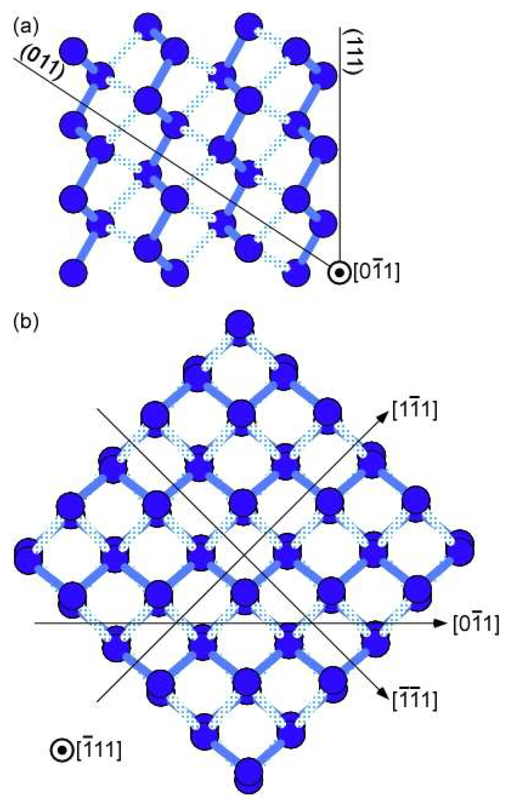
The finding that the dislocations were mostly edge dislocations could be interpreted in terms of the Peierls stress. Bi1−xSbx with a rhombohedral crystal structure has a cleavage on the plane. Figure 6a,b shows the atomic structure of Bi1−xSbx viewed along the and directions, respectively. The direction is tilted from the normal direction of the slip plane toward the direction. Atomic planes parallel to the plane are arranged in double layers as shown in Figure 6a. The interatomic distance in a double layer is shorter than that between adjacent double layers [21]. Therefore, in the plane, the interatomic distance along the direction is larger than that along the direction. In addition, it can be assumed that the shorter bonds are stronger and the longer bonds are weaker. Thus, the Peierls stress along the direction should be higher than that along the direction. Accordingly, it can be considered that, for mobile dislocations in the plane, the edge segments along the direction, which are trapped along the valley of the Peierls potential, require higher stress to glide, thus leading to their lower mobility. In addition, dislocation segments along the and directions observed in Figure 4 are also expected to be stable because they are along the atomic columns as shown in Figure 6b. Resultant long dislocation segments are expected to have an advantage in dislocation conduction measurements. Furthermore, such long dislocations aligned in one direction may be useful for future device applications.
4. Conclusions
Bi1−xSbx single crystals, within the range of the TI phase with the invariants (1;111), were fabricated by a zone-melting method. The crystals were plastically deformed at room temperature. The compression axis was set at the direction to activate the slip system . As a result, high-density dislocations with a Burgers vector , satisfying the condition for the formation of gapless states, were introduced. The dislocations were mostly of edge type with lengths on the order of more than a few micrometers. For mobile dislocations in the plane, it can be considered that the edge segments along the direction require higher stress to glide, thus leading to their lower mobility. Resultant long dislocation segments aligned in one direction are expected to have an advantage in experimental investigations of the dislocation properties and future device fabrications.
Author Contributions
Conceptualization, Y.T. and K.E.; methodology, Y.T.; validation, Y.T.; investigation, Y.T. and R.F.; resources, Y.T.; writing—original draft preparation, Y.T.; writing—review and editing, Y.T. and K.E.; visualization, Y.T.; supervision, K.E.; project administration, Y.T. and K.E.; funding acquisition, Y.T. and K.E.
Funding
This work was financially supported by Japan Society for the Promotion of Science (JSPS) KAKENHI (Grant No. 18H01692 and 19K04984) and Iketani Science and Technology Foundation (0301060-A).
Acknowledgments
A part of this work was conducted at Advanced Characterization Nanotechnology Platform of the University of Tokyo, supported by “Nanotechnology Platform” of the Ministry of Education, Culture, Sports, Science and Technology (MEXT), Japan.
Conflicts of Interest
The authors declare no conflict of interest.
References
- Hasan, M.Z.; Kane, C.L. Topological insulators. Rev. Mod. Phys. 2010, 82, 3045–3067. [Google Scholar] [CrossRef]
- Ando, Y. Topological insulator materials. J. Phys. Soc. Jpn. 2013, 82, 102001. [Google Scholar] [CrossRef]
- Ran, Y.; Zhang, Y.; Vishwanath, A. One-dimensional topologically protected modes in topological insulators with lattice dislocations. Nat. Phys. 2009, 5, 298–303. [Google Scholar] [CrossRef] [Green Version]
- Moore, J.E.; Balents, L. Topological invariants of time-reversal-invariant band structures. Phys. Rev. B 2007, 75, 121306. [Google Scholar] [CrossRef] [Green Version]
- Fu, L.; Kane, C.L.; Mele, E.J. Topological insulators in three dimensions. Phys. Rev. Lett. 2007, 98, 106803. [Google Scholar] [CrossRef] [PubMed]
- Tretiakov, O.A.; Abanov, A.; Murakami, S.; Sinova, J. Large thermoelectric figure of merit for three-dimensional topological Anderson insulators via line dislocation engineering. Appl. Phys. Lett. 2010, 97, 073108. [Google Scholar] [CrossRef] [Green Version]
- Fu, L.; Kane, C.L. Topological insulators with inversion symmetry. Phys. Rev. B 2007, 76, 045302. [Google Scholar] [CrossRef] [Green Version]
- Hsieh, D.; Qian, D.; Wray, L.; Xia, Y.; Hor, Y.S.; Cava, R.J.; Hasan, M.Z. A topological Dirac insulator in a quantum spin Hall phase. Nature 2008, 452, 970–974. [Google Scholar] [CrossRef] [Green Version]
- Ellett, M.R.; Horst, R.B.; Williams, L.R.; Cuff, K.F. Shubnikov-de Haas investigations of the Bi1−xSbx (0 < x < 0.3) system. J. Phys. Soc. Jpn. 1996, 21, 666–672. [Google Scholar]
- Imura, K.; Takane, Y.; Tanaka, A. Weak topological insulator with protected gapless helical states. Phys. Rev. B 2011, 84, 035443. [Google Scholar] [CrossRef]
- Yoshimura, Y.; Matsumoto, A.; Takane, Y.; Imura, K. Perfectly conducting channel on the dark surface of weak topological insulators. Phys. Rev. B 2013, 88, 045408. [Google Scholar] [CrossRef]
- Slager, R.-J.; Mesaros, A.; Juricic, V.; Zaanen, J. Interplay between electronic topology and crystal symmetry: Dislocation-line modes in topological band insulators. Phys. Rev. B 2014, 90, 241403. [Google Scholar] [CrossRef] [Green Version]
- Hamasaki, H.; Tokumoto, Y.; Edagawa, K. Dislocation conduction in Bi-Sb topological insulators. Appl. Phys. Lett. 2017, 110, 092105. [Google Scholar] [CrossRef] [Green Version]
- Otake, S.; Motohashi, Y. Plastic deformation and dislocation etch-pit distribution for the primary glide system on bismuth single crystals. J. Jpn. Inst. Met. Mater. 1973, 37, 44–51. [Google Scholar] [CrossRef]
- Motohashi, Y.; Otake, S. Plastic deformation and dislocation etch-pit distribution due to the glide system for bismuth single crystals. J. Jpn. Inst. Met. Mater. 1973, 37, 978–985. [Google Scholar] [CrossRef]
- Yanaka, Y.; Kariya, Y.; Watanabe, H.; Hokazono, H. Plastic deformation behavior and mechanism of bismuth single crystals in principal axes. Mater. Trans. 2016, 57, 819–823. [Google Scholar] [CrossRef]
- Yanaka, Y.; Kariya, Y.; Watanabe, H.; Hokazono, H. Influence of temperature on plastic deformation behavior and mechanism of bismuth single crystals. J. Electron. Mater. 2018, 47, 594–603. [Google Scholar] [CrossRef]
- Otake, S.; Namazuea, H.; Matsuno, N. Critical resolved shear stresses of two slip systems in bismuth single crystals. Jpn. J. Appl. Phys. 1980, 19, 433–437. [Google Scholar] [CrossRef]
- Steegmuller, C.; Daniel, J.S. Slip in bismuth. J. Less Common Met. 1972, 27, 81–85. [Google Scholar] [CrossRef]
- Matsuo, T.; Suzuki, H. Effect of plastic deformation on the thermal conductivity of bismuth crystals. J. Phys. Soc. Jpn. 1976, 41, 1692–1698. [Google Scholar] [CrossRef]
- Mooser, E.; Peason, W.B. The crystal structures and properties of the group VB to VIIB elements and of compounds formed between them. J. Phys. Chem. Solids 1958, 7, 65–77. [Google Scholar] [CrossRef]
Figure 1.
Schematic illustration of the sample for plastic deformations.

Figure 2.
Electron probe microanalyzer (EPMA) line profiles of Sb concentrations obtained for the grown crystal. (a) EPMA line profile along the crystal growth direction; (b) EPMA line profile perpendicular to the crystal growth direction.
Figure 2.
Electron probe microanalyzer (EPMA) line profiles of Sb concentrations obtained for the grown crystal. (a) EPMA line profile along the crystal growth direction; (b) EPMA line profile perpendicular to the crystal growth direction.

Figure 3.
Stress–strain curve of the bismuth antimony (Bi1−xSbx) sample deformed at room temperature under a constant strain rate of 1 × 10⁻⁵ s−1. The Sb concentration of the deformed sample was in the range of 8.6–9.8 at%.
Figure 3.
Stress–strain curve of the bismuth antimony (Bi1−xSbx) sample deformed at room temperature under a constant strain rate of 1 × 10⁻⁵ s−1. The Sb concentration of the deformed sample was in the range of 8.6–9.8 at%.

Figure 4.
(a) TEM bright-field images obtained from the specimen cut out from the deformed sample; (b) the same images as in (a). Dislocations along the direction are indicated by red lines and dislocations that deviate from the direction more than are indicated by blue lines; (c) stereographic projection of Bi1−xSbx.

Figure 5.
(a) TEM bright-field image obtained from the specimen cut out from the deformed sample; (b) TEM dark-field image obtained using ; (c) TEM dark-field image obtained using .
Figure 5.
(a) TEM bright-field image obtained from the specimen cut out from the deformed sample; (b) TEM dark-field image obtained using ; (c) TEM dark-field image obtained using .

Figure 6.
(a) Schematic illustration showing the atomic structure of Bi1−xSbx viewed along the direction; (b) schematic illustration showing the atomic structure of Bi1−xSbx viewed along the direction which is tilted from the normal direction of the slip plane toward the direction. Shorter and longer bonds are represented by blue and light blue lines, respectively.

© 2019 by the authors. Licensee MDPI, Basel, Switzerland. This article is an open access article distributed under the terms and conditions of the Creative Commons Attribution (CC BY) license (http://creativecommons.org/licenses/by/4.0/).
Share and Cite
MDPI and ACS Style
Tokumoto, Y.; Fujiwara, R.; Edagawa, K. High-Density Well-Aligned Dislocations Introduced by Plastic Deformation in Bi1−xSbx Topological Insulator Single Crystals. Crystals 2019, 9, 317. https://0-doi-org.brum.beds.ac.uk/10.3390/cryst9060317
AMA Style
Tokumoto Y, Fujiwara R, Edagawa K. High-Density Well-Aligned Dislocations Introduced by Plastic Deformation in Bi1−xSbx Topological Insulator Single Crystals. Crystals. 2019; 9(6):317. https://0-doi-org.brum.beds.ac.uk/10.3390/cryst9060317
Chicago/Turabian StyleTokumoto, Yuki, Riku Fujiwara, and Keiichi Edagawa. 2019. "High-Density Well-Aligned Dislocations Introduced by Plastic Deformation in Bi1−xSbx Topological Insulator Single Crystals" Crystals 9, no. 6: 317. https://0-doi-org.brum.beds.ac.uk/10.3390/cryst9060317
Note that from the first issue of 2016, this journal uses article numbers instead of page numbers. See further details here.